JP2007041237A - Method of manufacturing color filter, color filter and liquid crystal display device - Google Patents
Method of manufacturing color filter, color filter and liquid crystal display device Download PDFInfo
- Publication number
- JP2007041237A JP2007041237A JP2005224727A JP2005224727A JP2007041237A JP 2007041237 A JP2007041237 A JP 2007041237A JP 2005224727 A JP2005224727 A JP 2005224727A JP 2005224727 A JP2005224727 A JP 2005224727A JP 2007041237 A JP2007041237 A JP 2007041237A
- Authority
- JP
- Japan
- Prior art keywords
- liquid crystal
- color filter
- layer
- exposure
- resin layer
- Prior art date
- Legal status (The legal status is an assumption and is not a legal conclusion. Google has not performed a legal analysis and makes no representation as to the accuracy of the status listed.)
- Abandoned
Links
- 239000004973 liquid crystal related substance Substances 0.000 title claims abstract description 120
- 238000004519 manufacturing process Methods 0.000 title claims abstract description 27
- 239000011342 resin composition Substances 0.000 claims abstract description 20
- 239000000758 substrate Substances 0.000 claims description 112
- 229920005989 resin Polymers 0.000 claims description 110
- 239000011347 resin Substances 0.000 claims description 110
- 239000000463 material Substances 0.000 claims description 80
- 238000012546 transfer Methods 0.000 claims description 73
- 238000000034 method Methods 0.000 claims description 69
- QVEIBLDXZNGPHR-UHFFFAOYSA-N naphthalene-1,4-dione;diazide Chemical class [N-]=[N+]=[N-].[N-]=[N+]=[N-].C1=CC=C2C(=O)C=CC(=O)C2=C1 QVEIBLDXZNGPHR-UHFFFAOYSA-N 0.000 claims description 7
- 239000005011 phenolic resin Substances 0.000 claims description 4
- 239000010410 layer Substances 0.000 description 286
- 239000013307 optical fiber Substances 0.000 description 72
- 229920005992 thermoplastic resin Polymers 0.000 description 55
- -1 naphthoquinone diazide ester Chemical class 0.000 description 50
- 239000010408 film Substances 0.000 description 40
- ZWEHNKRNPOVVGH-UHFFFAOYSA-N 2-Butanone Chemical compound CCC(C)=O ZWEHNKRNPOVVGH-UHFFFAOYSA-N 0.000 description 39
- 238000000576 coating method Methods 0.000 description 33
- 239000011248 coating agent Substances 0.000 description 31
- 239000000243 solution Substances 0.000 description 26
- 239000004065 semiconductor Substances 0.000 description 25
- 239000000203 mixture Substances 0.000 description 24
- 238000005253 cladding Methods 0.000 description 21
- 239000000835 fiber Substances 0.000 description 21
- 230000003287 optical effect Effects 0.000 description 21
- 239000000126 substance Substances 0.000 description 20
- QTWJRLJHJPIABL-UHFFFAOYSA-N 2-methylphenol;3-methylphenol;4-methylphenol Chemical compound CC1=CC=C(O)C=C1.CC1=CC=CC(O)=C1.CC1=CC=CC=C1O QTWJRLJHJPIABL-UHFFFAOYSA-N 0.000 description 17
- 229930003836 cresol Natural products 0.000 description 17
- 239000000975 dye Substances 0.000 description 17
- ISWSIDIOOBJBQZ-UHFFFAOYSA-N Phenol Chemical compound OC1=CC=CC=C1 ISWSIDIOOBJBQZ-UHFFFAOYSA-N 0.000 description 16
- OKKJLVBELUTLKV-UHFFFAOYSA-N Methanol Chemical compound OC OKKJLVBELUTLKV-UHFFFAOYSA-N 0.000 description 15
- LYCAIKOWRPUZTN-UHFFFAOYSA-N ethylene glycol Natural products OCCO LYCAIKOWRPUZTN-UHFFFAOYSA-N 0.000 description 15
- 238000010438 heat treatment Methods 0.000 description 14
- 230000001681 protective effect Effects 0.000 description 14
- 239000007864 aqueous solution Substances 0.000 description 13
- 239000011230 binding agent Substances 0.000 description 13
- 239000011521 glass Substances 0.000 description 13
- 239000000049 pigment Substances 0.000 description 13
- 239000002904 solvent Substances 0.000 description 13
- 238000011161 development Methods 0.000 description 12
- 230000018109 developmental process Effects 0.000 description 12
- 230000008569 process Effects 0.000 description 12
- LFQSCWFLJHTTHZ-UHFFFAOYSA-N Ethanol Chemical compound CCO LFQSCWFLJHTTHZ-UHFFFAOYSA-N 0.000 description 10
- 229920001577 copolymer Polymers 0.000 description 10
- 239000010419 fine particle Substances 0.000 description 10
- 239000003960 organic solvent Substances 0.000 description 10
- CSCPPACGZOOCGX-UHFFFAOYSA-N Acetone Chemical compound CC(C)=O CSCPPACGZOOCGX-UHFFFAOYSA-N 0.000 description 9
- CERQOIWHTDAKMF-UHFFFAOYSA-N Methacrylic acid Chemical class CC(=C)C(O)=O CERQOIWHTDAKMF-UHFFFAOYSA-N 0.000 description 9
- AOJOEFVRHOZDFN-UHFFFAOYSA-N benzyl 2-methylprop-2-enoate Chemical compound CC(=C)C(=O)OCC1=CC=CC=C1 AOJOEFVRHOZDFN-UHFFFAOYSA-N 0.000 description 9
- 150000001875 compounds Chemical class 0.000 description 9
- XTHFKEDIFFGKHM-UHFFFAOYSA-N Dimethoxyethane Chemical compound COCCOC XTHFKEDIFFGKHM-UHFFFAOYSA-N 0.000 description 8
- PPBRXRYQALVLMV-UHFFFAOYSA-N Styrene Chemical compound C=CC1=CC=CC=C1 PPBRXRYQALVLMV-UHFFFAOYSA-N 0.000 description 8
- 238000007334 copolymerization reaction Methods 0.000 description 8
- 239000006185 dispersion Substances 0.000 description 8
- 230000000694 effects Effects 0.000 description 8
- 229910044991 metal oxide Inorganic materials 0.000 description 8
- 150000004706 metal oxides Chemical class 0.000 description 8
- 229920000642 polymer Polymers 0.000 description 8
- 238000012545 processing Methods 0.000 description 8
- 125000006850 spacer group Chemical group 0.000 description 8
- VYPSYNLAJGMNEJ-UHFFFAOYSA-N Silicium dioxide Chemical compound O=[Si]=O VYPSYNLAJGMNEJ-UHFFFAOYSA-N 0.000 description 7
- 229920001600 hydrophobic polymer Polymers 0.000 description 7
- 239000007788 liquid Substances 0.000 description 7
- QSHDDOUJBYECFT-UHFFFAOYSA-N mercury Chemical compound [Hg] QSHDDOUJBYECFT-UHFFFAOYSA-N 0.000 description 7
- 230000002829 reductive effect Effects 0.000 description 7
- 230000007261 regionalization Effects 0.000 description 7
- XLYOFNOQVPJJNP-UHFFFAOYSA-N water Substances O XLYOFNOQVPJJNP-UHFFFAOYSA-N 0.000 description 7
- XEKOWRVHYACXOJ-UHFFFAOYSA-N Ethyl acetate Chemical compound CCOC(C)=O XEKOWRVHYACXOJ-UHFFFAOYSA-N 0.000 description 6
- OFOBLEOULBTSOW-UHFFFAOYSA-N Malonic acid Chemical compound OC(=O)CC(O)=O OFOBLEOULBTSOW-UHFFFAOYSA-N 0.000 description 6
- ZMXDDKWLCZADIW-UHFFFAOYSA-N N,N-Dimethylformamide Chemical compound CN(C)C=O ZMXDDKWLCZADIW-UHFFFAOYSA-N 0.000 description 6
- YXFVVABEGXRONW-UHFFFAOYSA-N Toluene Chemical compound CC1=CC=CC=C1 YXFVVABEGXRONW-UHFFFAOYSA-N 0.000 description 6
- XLOMVQKBTHCTTD-UHFFFAOYSA-N Zinc monoxide Chemical compound [Zn]=O XLOMVQKBTHCTTD-UHFFFAOYSA-N 0.000 description 6
- MPIAGWXWVAHQBB-UHFFFAOYSA-N [3-prop-2-enoyloxy-2-[[3-prop-2-enoyloxy-2,2-bis(prop-2-enoyloxymethyl)propoxy]methyl]-2-(prop-2-enoyloxymethyl)propyl] prop-2-enoate Chemical compound C=CC(=O)OCC(COC(=O)C=C)(COC(=O)C=C)COCC(COC(=O)C=C)(COC(=O)C=C)COC(=O)C=C MPIAGWXWVAHQBB-UHFFFAOYSA-N 0.000 description 6
- 238000007792 addition Methods 0.000 description 6
- 239000003431 cross linking reagent Substances 0.000 description 6
- JHIVVAPYMSGYDF-UHFFFAOYSA-N cyclohexanone Chemical compound O=C1CCCCC1 JHIVVAPYMSGYDF-UHFFFAOYSA-N 0.000 description 6
- 239000002270 dispersing agent Substances 0.000 description 6
- 230000001965 increasing effect Effects 0.000 description 6
- 238000010030 laminating Methods 0.000 description 6
- 239000011159 matrix material Substances 0.000 description 6
- 229910052753 mercury Inorganic materials 0.000 description 6
- 229920000036 polyvinylpyrrolidone Polymers 0.000 description 6
- 235000013855 polyvinylpyrrolidone Nutrition 0.000 description 6
- 229920005604 random copolymer Polymers 0.000 description 6
- GHMLBKRAJCXXBS-UHFFFAOYSA-N resorcinol Chemical compound OC1=CC=CC(O)=C1 GHMLBKRAJCXXBS-UHFFFAOYSA-N 0.000 description 6
- CDBYLPFSWZWCQE-UHFFFAOYSA-L Sodium Carbonate Chemical compound [Na+].[Na+].[O-]C([O-])=O CDBYLPFSWZWCQE-UHFFFAOYSA-L 0.000 description 5
- 239000000654 additive Substances 0.000 description 5
- 239000003513 alkali Substances 0.000 description 5
- 238000003491 array Methods 0.000 description 5
- 239000003795 chemical substances by application Substances 0.000 description 5
- 239000002131 composite material Substances 0.000 description 5
- 230000001276 controlling effect Effects 0.000 description 5
- 230000007547 defect Effects 0.000 description 5
- 238000001514 detection method Methods 0.000 description 5
- 239000007789 gas Substances 0.000 description 5
- 229920000620 organic polymer Polymers 0.000 description 5
- 235000013824 polyphenols Nutrition 0.000 description 5
- 239000001267 polyvinylpyrrolidone Substances 0.000 description 5
- 239000000047 product Substances 0.000 description 5
- 150000003839 salts Chemical class 0.000 description 5
- 239000007787 solid Substances 0.000 description 5
- 238000011282 treatment Methods 0.000 description 5
- SVONRAPFKPVNKG-UHFFFAOYSA-N 2-ethoxyethyl acetate Chemical compound CCOCCOC(C)=O SVONRAPFKPVNKG-UHFFFAOYSA-N 0.000 description 4
- YEJRWHAVMIAJKC-UHFFFAOYSA-N 4-Butyrolactone Chemical compound O=C1CCCO1 YEJRWHAVMIAJKC-UHFFFAOYSA-N 0.000 description 4
- XKRFYHLGVUSROY-UHFFFAOYSA-N Argon Chemical compound [Ar] XKRFYHLGVUSROY-UHFFFAOYSA-N 0.000 description 4
- CURLTUGMZLYLDI-UHFFFAOYSA-N Carbon dioxide Chemical compound O=C=O CURLTUGMZLYLDI-UHFFFAOYSA-N 0.000 description 4
- 108010010803 Gelatin Proteins 0.000 description 4
- 229920003171 Poly (ethylene oxide) Polymers 0.000 description 4
- 239000004952 Polyamide Substances 0.000 description 4
- 239000004372 Polyvinyl alcohol Substances 0.000 description 4
- UIIMBOGNXHQVGW-UHFFFAOYSA-M Sodium bicarbonate Chemical compound [Na+].OC([O-])=O UIIMBOGNXHQVGW-UHFFFAOYSA-M 0.000 description 4
- WYURNTSHIVDZCO-UHFFFAOYSA-N Tetrahydrofuran Chemical compound C1CCOC1 WYURNTSHIVDZCO-UHFFFAOYSA-N 0.000 description 4
- 229940022663 acetate Drugs 0.000 description 4
- 230000000996 additive effect Effects 0.000 description 4
- 229910052783 alkali metal Inorganic materials 0.000 description 4
- QVGXLLKOCUKJST-UHFFFAOYSA-N atomic oxygen Chemical compound [O] QVGXLLKOCUKJST-UHFFFAOYSA-N 0.000 description 4
- 230000005540 biological transmission Effects 0.000 description 4
- PXKLMJQFEQBVLD-UHFFFAOYSA-N bisphenol F Chemical compound C1=CC(O)=CC=C1CC1=CC=C(O)C=C1 PXKLMJQFEQBVLD-UHFFFAOYSA-N 0.000 description 4
- MTHSVFCYNBDYFN-UHFFFAOYSA-N diethylene glycol Chemical class OCCOCCO MTHSVFCYNBDYFN-UHFFFAOYSA-N 0.000 description 4
- SBZXBUIDTXKZTM-UHFFFAOYSA-N diglyme Chemical compound COCCOCCOC SBZXBUIDTXKZTM-UHFFFAOYSA-N 0.000 description 4
- 238000009826 distribution Methods 0.000 description 4
- 239000000428 dust Substances 0.000 description 4
- LZCLXQDLBQLTDK-UHFFFAOYSA-N ethyl 2-hydroxypropanoate Chemical compound CCOC(=O)C(C)O LZCLXQDLBQLTDK-UHFFFAOYSA-N 0.000 description 4
- BHXIWUJLHYHGSJ-UHFFFAOYSA-N ethyl 3-ethoxypropanoate Chemical compound CCOCCC(=O)OCC BHXIWUJLHYHGSJ-UHFFFAOYSA-N 0.000 description 4
- 125000001495 ethyl group Chemical group [H]C([H])([H])C([H])([H])* 0.000 description 4
- 238000011156 evaluation Methods 0.000 description 4
- 229920000159 gelatin Polymers 0.000 description 4
- 239000008273 gelatin Substances 0.000 description 4
- 235000019322 gelatine Nutrition 0.000 description 4
- 235000011852 gelatine desserts Nutrition 0.000 description 4
- FUZZWVXGSFPDMH-UHFFFAOYSA-N hexanoic acid Chemical compound CCCCCC(O)=O FUZZWVXGSFPDMH-UHFFFAOYSA-N 0.000 description 4
- WGCNASOHLSPBMP-UHFFFAOYSA-N hydroxyacetaldehyde Natural products OCC=O WGCNASOHLSPBMP-UHFFFAOYSA-N 0.000 description 4
- 150000002576 ketones Chemical class 0.000 description 4
- JVTAAEKCZFNVCJ-UHFFFAOYSA-N lactic acid Chemical compound CC(O)C(O)=O JVTAAEKCZFNVCJ-UHFFFAOYSA-N 0.000 description 4
- 238000003475 lamination Methods 0.000 description 4
- BDJSOPWXYLFTNW-UHFFFAOYSA-N methyl 3-methoxypropanoate Chemical compound COCCC(=O)OC BDJSOPWXYLFTNW-UHFFFAOYSA-N 0.000 description 4
- 239000001301 oxygen Substances 0.000 description 4
- 229910052760 oxygen Inorganic materials 0.000 description 4
- 238000000059 patterning Methods 0.000 description 4
- 229920003023 plastic Polymers 0.000 description 4
- 239000004033 plastic Substances 0.000 description 4
- 239000000088 plastic resin Substances 0.000 description 4
- 229920002647 polyamide Polymers 0.000 description 4
- 229920000728 polyester Polymers 0.000 description 4
- 229920002451 polyvinyl alcohol Polymers 0.000 description 4
- BWHMMNNQKKPAPP-UHFFFAOYSA-L potassium carbonate Chemical compound [K+].[K+].[O-]C([O-])=O BWHMMNNQKKPAPP-UHFFFAOYSA-L 0.000 description 4
- 229910052913 potassium silicate Inorganic materials 0.000 description 4
- 235000019353 potassium silicate Nutrition 0.000 description 4
- WQGWDDDVZFFDIG-UHFFFAOYSA-N pyrogallol Chemical compound OC1=CC=CC(O)=C1O WQGWDDDVZFFDIG-UHFFFAOYSA-N 0.000 description 4
- 230000035945 sensitivity Effects 0.000 description 4
- 229910052911 sodium silicate Inorganic materials 0.000 description 4
- 239000010409 thin film Substances 0.000 description 4
- VZCYOOQTPOCHFL-UHFFFAOYSA-N trans-butenedioic acid Natural products OC(=O)C=CC(O)=O VZCYOOQTPOCHFL-UHFFFAOYSA-N 0.000 description 4
- ZRDYULMDEGRWRC-UHFFFAOYSA-N (4-hydroxyphenyl)-(2,3,4-trihydroxyphenyl)methanone Chemical compound C1=CC(O)=CC=C1C(=O)C1=CC=C(O)C(O)=C1O ZRDYULMDEGRWRC-UHFFFAOYSA-N 0.000 description 3
- WJFKNYWRSNBZNX-UHFFFAOYSA-N 10H-phenothiazine Chemical compound C1=CC=C2NC3=CC=CC=C3SC2=C1 WJFKNYWRSNBZNX-UHFFFAOYSA-N 0.000 description 3
- XNWFRZJHXBZDAG-UHFFFAOYSA-N 2-METHOXYETHANOL Chemical compound COCCO XNWFRZJHXBZDAG-UHFFFAOYSA-N 0.000 description 3
- ZNQVEEAIQZEUHB-UHFFFAOYSA-N 2-ethoxyethanol Chemical compound CCOCCO ZNQVEEAIQZEUHB-UHFFFAOYSA-N 0.000 description 3
- QTBSBXVTEAMEQO-UHFFFAOYSA-M Acetate Chemical compound CC([O-])=O QTBSBXVTEAMEQO-UHFFFAOYSA-M 0.000 description 3
- SDDLEVPIDBLVHC-UHFFFAOYSA-N Bisphenol Z Chemical compound C1=CC(O)=CC=C1C1(C=2C=CC(O)=CC=2)CCCCC1 SDDLEVPIDBLVHC-UHFFFAOYSA-N 0.000 description 3
- WSFSSNUMVMOOMR-UHFFFAOYSA-N Formaldehyde Chemical compound O=C WSFSSNUMVMOOMR-UHFFFAOYSA-N 0.000 description 3
- KFZMGEQAYNKOFK-UHFFFAOYSA-N Isopropanol Chemical compound CC(C)O KFZMGEQAYNKOFK-UHFFFAOYSA-N 0.000 description 3
- VVQNEPGJFQJSBK-UHFFFAOYSA-N Methyl methacrylate Chemical compound COC(=O)C(C)=C VVQNEPGJFQJSBK-UHFFFAOYSA-N 0.000 description 3
- KWYUFKZDYYNOTN-UHFFFAOYSA-M Potassium hydroxide Chemical compound [OH-].[K+] KWYUFKZDYYNOTN-UHFFFAOYSA-M 0.000 description 3
- DNIAPMSPPWPWGF-UHFFFAOYSA-N Propylene glycol Chemical compound CC(O)CO DNIAPMSPPWPWGF-UHFFFAOYSA-N 0.000 description 3
- 239000004115 Sodium Silicate Substances 0.000 description 3
- HEMHJVSKTPXQMS-UHFFFAOYSA-M Sodium hydroxide Chemical compound [OH-].[Na+] HEMHJVSKTPXQMS-UHFFFAOYSA-M 0.000 description 3
- KDYFGRWQOYBRFD-UHFFFAOYSA-N Succinic acid Natural products OC(=O)CCC(O)=O KDYFGRWQOYBRFD-UHFFFAOYSA-N 0.000 description 3
- GWEVSGVZZGPLCZ-UHFFFAOYSA-N Titan oxide Chemical compound O=[Ti]=O GWEVSGVZZGPLCZ-UHFFFAOYSA-N 0.000 description 3
- RTAQQCXQSZGOHL-UHFFFAOYSA-N Titanium Chemical compound [Ti] RTAQQCXQSZGOHL-UHFFFAOYSA-N 0.000 description 3
- GSEJCLTVZPLZKY-UHFFFAOYSA-N Triethanolamine Chemical compound OCCN(CCO)CCO GSEJCLTVZPLZKY-UHFFFAOYSA-N 0.000 description 3
- 239000000853 adhesive Substances 0.000 description 3
- 230000001070 adhesive effect Effects 0.000 description 3
- 150000007933 aliphatic carboxylic acids Chemical class 0.000 description 3
- 229910052782 aluminium Inorganic materials 0.000 description 3
- QVQLCTNNEUAWMS-UHFFFAOYSA-N barium oxide Chemical compound [Ba]=O QVQLCTNNEUAWMS-UHFFFAOYSA-N 0.000 description 3
- 229920002678 cellulose Polymers 0.000 description 3
- 230000008859 change Effects 0.000 description 3
- 239000007795 chemical reaction product Substances 0.000 description 3
- 238000004040 coloring Methods 0.000 description 3
- 239000004020 conductor Substances 0.000 description 3
- 230000008878 coupling Effects 0.000 description 3
- 238000010168 coupling process Methods 0.000 description 3
- 238000005859 coupling reaction Methods 0.000 description 3
- SWXVUIWOUIDPGS-UHFFFAOYSA-N diacetone alcohol Chemical class CC(=O)CC(C)(C)O SWXVUIWOUIDPGS-UHFFFAOYSA-N 0.000 description 3
- 235000014113 dietary fatty acids Nutrition 0.000 description 3
- 208000028659 discharge Diseases 0.000 description 3
- 238000001035 drying Methods 0.000 description 3
- 150000002148 esters Chemical class 0.000 description 3
- 150000002170 ethers Chemical class 0.000 description 3
- 239000000194 fatty acid Substances 0.000 description 3
- 229930195729 fatty acid Natural products 0.000 description 3
- 238000010304 firing Methods 0.000 description 3
- 230000006870 function Effects 0.000 description 3
- 125000002887 hydroxy group Chemical group [H]O* 0.000 description 3
- 230000001771 impaired effect Effects 0.000 description 3
- 238000009434 installation Methods 0.000 description 3
- 230000001678 irradiating effect Effects 0.000 description 3
- CPLXHLVBOLITMK-UHFFFAOYSA-N magnesium oxide Inorganic materials [Mg]=O CPLXHLVBOLITMK-UHFFFAOYSA-N 0.000 description 3
- 229940107698 malachite green Drugs 0.000 description 3
- FDZZZRQASAIRJF-UHFFFAOYSA-M malachite green Chemical compound [Cl-].C1=CC(N(C)C)=CC=C1C(C=1C=CC=CC=1)=C1C=CC(=[N+](C)C)C=C1 FDZZZRQASAIRJF-UHFFFAOYSA-M 0.000 description 3
- 238000000465 moulding Methods 0.000 description 3
- 229910052757 nitrogen Inorganic materials 0.000 description 3
- 239000002736 nonionic surfactant Substances 0.000 description 3
- 229920003986 novolac Polymers 0.000 description 3
- 239000002245 particle Substances 0.000 description 3
- 229950000688 phenothiazine Drugs 0.000 description 3
- 239000004014 plasticizer Substances 0.000 description 3
- BDERNNFJNOPAEC-UHFFFAOYSA-N propan-1-ol Chemical compound CCCO BDERNNFJNOPAEC-UHFFFAOYSA-N 0.000 description 3
- NTHWMYGWWRZVTN-UHFFFAOYSA-N sodium silicate Chemical compound [Na+].[Na+].[O-][Si]([O-])=O NTHWMYGWWRZVTN-UHFFFAOYSA-N 0.000 description 3
- 238000005507 spraying Methods 0.000 description 3
- 239000004094 surface-active agent Substances 0.000 description 3
- XOLBLPGZBRYERU-UHFFFAOYSA-N tin dioxide Chemical compound O=[Sn]=O XOLBLPGZBRYERU-UHFFFAOYSA-N 0.000 description 3
- 238000011144 upstream manufacturing Methods 0.000 description 3
- 239000011787 zinc oxide Substances 0.000 description 3
- QYGBYAQGBVHMDD-XQRVVYSFSA-N (z)-2-cyano-3-thiophen-2-ylprop-2-enoic acid Chemical compound OC(=O)C(\C#N)=C/C1=CC=CS1 QYGBYAQGBVHMDD-XQRVVYSFSA-N 0.000 description 2
- KBPLFHHGFOOTCA-UHFFFAOYSA-N 1-Octanol Chemical compound CCCCCCCCO KBPLFHHGFOOTCA-UHFFFAOYSA-N 0.000 description 2
- RRQYJINTUHWNHW-UHFFFAOYSA-N 1-ethoxy-2-(2-ethoxyethoxy)ethane Chemical compound CCOCCOCCOCC RRQYJINTUHWNHW-UHFFFAOYSA-N 0.000 description 2
- CAQYAZNFWDDMIT-UHFFFAOYSA-N 1-ethoxy-2-methoxyethane Chemical compound CCOCCOC CAQYAZNFWDDMIT-UHFFFAOYSA-N 0.000 description 2
- LIPRQQHINVWJCH-UHFFFAOYSA-N 1-ethoxypropan-2-yl acetate Chemical compound CCOCC(C)OC(C)=O LIPRQQHINVWJCH-UHFFFAOYSA-N 0.000 description 2
- KUFFULVDNCHOFZ-UHFFFAOYSA-N 2,4-xylenol Chemical compound CC1=CC=C(O)C(C)=C1 KUFFULVDNCHOFZ-UHFFFAOYSA-N 0.000 description 2
- OJVAMHKKJGICOG-UHFFFAOYSA-N 2,5-hexanedione Chemical compound CC(=O)CCC(C)=O OJVAMHKKJGICOG-UHFFFAOYSA-N 0.000 description 2
- SBASXUCJHJRPEV-UHFFFAOYSA-N 2-(2-methoxyethoxy)ethanol Chemical compound COCCOCCO SBASXUCJHJRPEV-UHFFFAOYSA-N 0.000 description 2
- OEPOKWHJYJXUGD-UHFFFAOYSA-N 2-(3-phenylmethoxyphenyl)-1,3-thiazole-4-carbaldehyde Chemical compound O=CC1=CSC(C=2C=C(OCC=3C=CC=CC=3)C=CC=2)=N1 OEPOKWHJYJXUGD-UHFFFAOYSA-N 0.000 description 2
- HZAXFHJVJLSVMW-UHFFFAOYSA-N 2-Aminoethan-1-ol Chemical compound NCCO HZAXFHJVJLSVMW-UHFFFAOYSA-N 0.000 description 2
- WNIBOEDSTLUPQG-UHFFFAOYSA-N 2-[2-[4-(2-phenylethenyl)phenyl]ethenyl]-5-(trichloromethyl)-1,3,4-oxadiazole Chemical compound O1C(C(Cl)(Cl)Cl)=NN=C1C=CC(C=C1)=CC=C1C=CC1=CC=CC=C1 WNIBOEDSTLUPQG-UHFFFAOYSA-N 0.000 description 2
- TUBNHXBTFDDYPI-UHFFFAOYSA-N 2-cyclohexyl-4-[(5-cyclohexyl-4-hydroxy-2-methylphenyl)-(4-hydroxyphenyl)methyl]-5-methylphenol Chemical compound CC1=CC(O)=C(C2CCCCC2)C=C1C(C=1C(=CC(O)=C(C2CCCCC2)C=1)C)C1=CC=C(O)C=C1 TUBNHXBTFDDYPI-UHFFFAOYSA-N 0.000 description 2
- XLLIQLLCWZCATF-UHFFFAOYSA-N 2-methoxyethyl acetate Chemical compound COCCOC(C)=O XLLIQLLCWZCATF-UHFFFAOYSA-N 0.000 description 2
- RXNYJUSEXLAVNQ-UHFFFAOYSA-N 4,4'-Dihydroxybenzophenone Chemical compound C1=CC(O)=CC=C1C(=O)C1=CC=C(O)C=C1 RXNYJUSEXLAVNQ-UHFFFAOYSA-N 0.000 description 2
- NNLGOGUWIKXLCY-UHFFFAOYSA-N 4-(2-phenylpropan-2-yl)benzene-1,3-diol Chemical compound C=1C=C(O)C=C(O)C=1C(C)(C)C1=CC=CC=C1 NNLGOGUWIKXLCY-UHFFFAOYSA-N 0.000 description 2
- NPFYZDNDJHZQKY-UHFFFAOYSA-N 4-Hydroxybenzophenone Chemical compound C1=CC(O)=CC=C1C(=O)C1=CC=CC=C1 NPFYZDNDJHZQKY-UHFFFAOYSA-N 0.000 description 2
- SQYHCCZOOUAQOD-UHFFFAOYSA-N 5,8-dioxonaphthalene-1-sulfonyl chloride Chemical compound O=C1C=CC(=O)C2=C1C=CC=C2S(=O)(=O)Cl SQYHCCZOOUAQOD-UHFFFAOYSA-N 0.000 description 2
- DKPFZGUDAPQIHT-UHFFFAOYSA-N Butyl acetate Natural products CCCCOC(C)=O DKPFZGUDAPQIHT-UHFFFAOYSA-N 0.000 description 2
- RTZKZFJDLAIYFH-UHFFFAOYSA-N Diethyl ether Chemical compound CCOCC RTZKZFJDLAIYFH-UHFFFAOYSA-N 0.000 description 2
- IAZDPXIOMUYVGZ-UHFFFAOYSA-N Dimethylsulphoxide Chemical compound CS(C)=O IAZDPXIOMUYVGZ-UHFFFAOYSA-N 0.000 description 2
- 239000004593 Epoxy Substances 0.000 description 2
- VZCYOOQTPOCHFL-OWOJBTEDSA-N Fumaric acid Chemical compound OC(=O)\C=C\C(O)=O VZCYOOQTPOCHFL-OWOJBTEDSA-N 0.000 description 2
- PEDCQBHIVMGVHV-UHFFFAOYSA-N Glycerine Chemical compound OCC(O)CO PEDCQBHIVMGVHV-UHFFFAOYSA-N 0.000 description 2
- QIGBRXMKCJKVMJ-UHFFFAOYSA-N Hydroquinone Chemical compound OC1=CC=C(O)C=C1 QIGBRXMKCJKVMJ-UHFFFAOYSA-N 0.000 description 2
- XYVQFUJDGOBPQI-UHFFFAOYSA-N Methyl-2-hydoxyisobutyric acid Chemical compound COC(=O)C(C)(C)O XYVQFUJDGOBPQI-UHFFFAOYSA-N 0.000 description 2
- YNAVUWVOSKDBBP-UHFFFAOYSA-N Morpholine Chemical compound C1COCCN1 YNAVUWVOSKDBBP-UHFFFAOYSA-N 0.000 description 2
- FXHOOIRPVKKKFG-UHFFFAOYSA-N N,N-Dimethylacetamide Chemical compound CN(C)C(C)=O FXHOOIRPVKKKFG-UHFFFAOYSA-N 0.000 description 2
- LRHPLDYGYMQRHN-UHFFFAOYSA-N N-Butanol Chemical compound CCCCO LRHPLDYGYMQRHN-UHFFFAOYSA-N 0.000 description 2
- SECXISVLQFMRJM-UHFFFAOYSA-N N-Methylpyrrolidone Chemical compound CN1CCCC1=O SECXISVLQFMRJM-UHFFFAOYSA-N 0.000 description 2
- WHNWPMSKXPGLAX-UHFFFAOYSA-N N-Vinyl-2-pyrrolidone Chemical compound C=CN1CCCC1=O WHNWPMSKXPGLAX-UHFFFAOYSA-N 0.000 description 2
- ATHHXGZTWNVVOU-UHFFFAOYSA-N N-methylformamide Chemical compound CNC=O ATHHXGZTWNVVOU-UHFFFAOYSA-N 0.000 description 2
- 239000000020 Nitrocellulose Substances 0.000 description 2
- 241000047703 Nonion Species 0.000 description 2
- CTQNGGLPUBDAKN-UHFFFAOYSA-N O-Xylene Chemical compound CC1=CC=CC=C1C CTQNGGLPUBDAKN-UHFFFAOYSA-N 0.000 description 2
- 229910019142 PO4 Inorganic materials 0.000 description 2
- JPYHHZQJCSQRJY-UHFFFAOYSA-N Phloroglucinol Natural products CCC=CCC=CCC=CCC=CCCCCC(=O)C1=C(O)C=C(O)C=C1O JPYHHZQJCSQRJY-UHFFFAOYSA-N 0.000 description 2
- 239000004698 Polyethylene Substances 0.000 description 2
- 239000004743 Polypropylene Substances 0.000 description 2
- 239000004111 Potassium silicate Substances 0.000 description 2
- BLRPTPMANUNPDV-UHFFFAOYSA-N Silane Chemical compound [SiH4] BLRPTPMANUNPDV-UHFFFAOYSA-N 0.000 description 2
- 229920002472 Starch Polymers 0.000 description 2
- XTXRWKRVRITETP-UHFFFAOYSA-N Vinyl acetate Chemical compound CC(=O)OC=C XTXRWKRVRITETP-UHFFFAOYSA-N 0.000 description 2
- BZHJMEDXRYGGRV-UHFFFAOYSA-N Vinyl chloride Chemical compound ClC=C BZHJMEDXRYGGRV-UHFFFAOYSA-N 0.000 description 2
- FJWGYAHXMCUOOM-QHOUIDNNSA-N [(2s,3r,4s,5r,6r)-2-[(2r,3r,4s,5r,6s)-4,5-dinitrooxy-2-(nitrooxymethyl)-6-[(2r,3r,4s,5r,6s)-4,5,6-trinitrooxy-2-(nitrooxymethyl)oxan-3-yl]oxyoxan-3-yl]oxy-3,5-dinitrooxy-6-(nitrooxymethyl)oxan-4-yl] nitrate Chemical compound O([C@@H]1O[C@@H]([C@H]([C@H](O[N+]([O-])=O)[C@H]1O[N+]([O-])=O)O[C@H]1[C@@H]([C@@H](O[N+]([O-])=O)[C@H](O[N+]([O-])=O)[C@@H](CO[N+]([O-])=O)O1)O[N+]([O-])=O)CO[N+](=O)[O-])[C@@H]1[C@@H](CO[N+]([O-])=O)O[C@@H](O[N+]([O-])=O)[C@H](O[N+]([O-])=O)[C@H]1O[N+]([O-])=O FJWGYAHXMCUOOM-QHOUIDNNSA-N 0.000 description 2
- 239000012190 activator Substances 0.000 description 2
- WNLRTRBMVRJNCN-UHFFFAOYSA-N adipic acid Chemical compound OC(=O)CCCCC(O)=O WNLRTRBMVRJNCN-UHFFFAOYSA-N 0.000 description 2
- 150000001298 alcohols Chemical class 0.000 description 2
- 229910000288 alkali metal carbonate Inorganic materials 0.000 description 2
- 150000008041 alkali metal carbonates Chemical class 0.000 description 2
- 229910052910 alkali metal silicate Inorganic materials 0.000 description 2
- 150000001340 alkali metals Chemical class 0.000 description 2
- 239000002216 antistatic agent Substances 0.000 description 2
- 239000003125 aqueous solvent Substances 0.000 description 2
- 229910052786 argon Inorganic materials 0.000 description 2
- 150000004945 aromatic hydrocarbons Chemical class 0.000 description 2
- 239000012298 atmosphere Substances 0.000 description 2
- 125000004429 atom Chemical group 0.000 description 2
- 239000002585 base Substances 0.000 description 2
- QUKGYYKBILRGFE-UHFFFAOYSA-N benzyl acetate Chemical compound CC(=O)OCC1=CC=CC=C1 QUKGYYKBILRGFE-UHFFFAOYSA-N 0.000 description 2
- 230000001588 bifunctional effect Effects 0.000 description 2
- IISBACLAFKSPIT-UHFFFAOYSA-N bisphenol A Chemical compound C=1C=C(O)C=CC=1C(C)(C)C1=CC=C(O)C=C1 IISBACLAFKSPIT-UHFFFAOYSA-N 0.000 description 2
- 238000009835 boiling Methods 0.000 description 2
- 239000001569 carbon dioxide Substances 0.000 description 2
- 229910002092 carbon dioxide Inorganic materials 0.000 description 2
- 125000004181 carboxyalkyl group Chemical class 0.000 description 2
- 230000001427 coherent effect Effects 0.000 description 2
- 230000000052 comparative effect Effects 0.000 description 2
- 238000005520 cutting process Methods 0.000 description 2
- 230000006378 damage Effects 0.000 description 2
- ZBCBWPMODOFKDW-UHFFFAOYSA-N diethanolamine Chemical compound OCCNCCO ZBCBWPMODOFKDW-UHFFFAOYSA-N 0.000 description 2
- 229940019778 diethylene glycol diethyl ether Drugs 0.000 description 2
- 229940028356 diethylene glycol monobutyl ether Drugs 0.000 description 2
- XXJWXESWEXIICW-UHFFFAOYSA-N diethylene glycol monoethyl ether Chemical compound CCOCCOCCO XXJWXESWEXIICW-UHFFFAOYSA-N 0.000 description 2
- 229940075557 diethylene glycol monoethyl ether Drugs 0.000 description 2
- 238000004090 dissolution Methods 0.000 description 2
- 239000012153 distilled water Substances 0.000 description 2
- JBKVHLHDHHXQEQ-UHFFFAOYSA-N epsilon-caprolactam Chemical compound O=C1CCCCCN1 JBKVHLHDHHXQEQ-UHFFFAOYSA-N 0.000 description 2
- CKSRFHWWBKRUKA-UHFFFAOYSA-N ethyl 2-ethoxyacetate Chemical compound CCOCC(=O)OCC CKSRFHWWBKRUKA-UHFFFAOYSA-N 0.000 description 2
- GFUIDHWFLMPAGY-UHFFFAOYSA-N ethyl 2-hydroxy-2-methylpropanoate Chemical compound CCOC(=O)C(C)(C)O GFUIDHWFLMPAGY-UHFFFAOYSA-N 0.000 description 2
- ZANNOFHADGWOLI-UHFFFAOYSA-N ethyl 2-hydroxyacetate Chemical compound CCOC(=O)CO ZANNOFHADGWOLI-UHFFFAOYSA-N 0.000 description 2
- MTZQAGJQAFMTAQ-UHFFFAOYSA-N ethyl benzoate Chemical compound CCOC(=O)C1=CC=CC=C1 MTZQAGJQAFMTAQ-UHFFFAOYSA-N 0.000 description 2
- 230000005284 excitation Effects 0.000 description 2
- PJXISJQVUVHSOJ-UHFFFAOYSA-N indium(iii) oxide Chemical compound [O-2].[O-2].[O-2].[In+3].[In+3] PJXISJQVUVHSOJ-UHFFFAOYSA-N 0.000 description 2
- 239000003112 inhibitor Substances 0.000 description 2
- HJOVHMDZYOCNQW-UHFFFAOYSA-N isophorone Chemical compound CC1=CC(=O)CC(C)(C)C1 HJOVHMDZYOCNQW-UHFFFAOYSA-N 0.000 description 2
- 239000000395 magnesium oxide Substances 0.000 description 2
- VZCYOOQTPOCHFL-UPHRSURJSA-N maleic acid Chemical compound OC(=O)\C=C/C(O)=O VZCYOOQTPOCHFL-UPHRSURJSA-N 0.000 description 2
- 239000011976 maleic acid Substances 0.000 description 2
- FPYJFEHAWHCUMM-UHFFFAOYSA-N maleic anhydride Chemical compound O=C1OC(=O)C=C1 FPYJFEHAWHCUMM-UHFFFAOYSA-N 0.000 description 2
- BJEPYKJPYRNKOW-UHFFFAOYSA-N malic acid Chemical compound OC(=O)C(O)CC(O)=O BJEPYKJPYRNKOW-UHFFFAOYSA-N 0.000 description 2
- 229910052751 metal Inorganic materials 0.000 description 2
- 239000002184 metal Substances 0.000 description 2
- VNWKTOKETHGBQD-UHFFFAOYSA-N methane Chemical compound C VNWKTOKETHGBQD-UHFFFAOYSA-N 0.000 description 2
- FMXYCZVOMYLMKM-UHFFFAOYSA-N methyl 2-hydroxy-2-methylbutanoate Chemical compound CCC(C)(O)C(=O)OC FMXYCZVOMYLMKM-UHFFFAOYSA-N 0.000 description 2
- HSDFKDZBJMDHFF-UHFFFAOYSA-N methyl 3-ethoxypropanoate Chemical compound CCOCCC(=O)OC HSDFKDZBJMDHFF-UHFFFAOYSA-N 0.000 description 2
- JKQOBWVOAYFWKG-UHFFFAOYSA-N molybdenum trioxide Chemical compound O=[Mo](=O)=O JKQOBWVOAYFWKG-UHFFFAOYSA-N 0.000 description 2
- 229910052758 niobium Inorganic materials 0.000 description 2
- 229920001220 nitrocellulos Polymers 0.000 description 2
- ZWRUINPWMLAQRD-UHFFFAOYSA-N nonan-1-ol Chemical compound CCCCCCCCCO ZWRUINPWMLAQRD-UHFFFAOYSA-N 0.000 description 2
- WWZKQHOCKIZLMA-UHFFFAOYSA-N octanoic acid Chemical compound CCCCCCCC(O)=O WWZKQHOCKIZLMA-UHFFFAOYSA-N 0.000 description 2
- 239000003921 oil Substances 0.000 description 2
- 239000005304 optical glass Substances 0.000 description 2
- 230000010355 oscillation Effects 0.000 description 2
- JCGNDDUYTRNOFT-UHFFFAOYSA-N oxolane-2,4-dione Chemical compound O=C1COC(=O)C1 JCGNDDUYTRNOFT-UHFFFAOYSA-N 0.000 description 2
- NWVVVBRKAWDGAB-UHFFFAOYSA-N p-methoxyphenol Chemical compound COC1=CC=C(O)C=C1 NWVVVBRKAWDGAB-UHFFFAOYSA-N 0.000 description 2
- XNLICIUVMPYHGG-UHFFFAOYSA-N pentan-2-one Chemical compound CCCC(C)=O XNLICIUVMPYHGG-UHFFFAOYSA-N 0.000 description 2
- 150000002989 phenols Chemical class 0.000 description 2
- WVDDGKGOMKODPV-ZQBYOMGUSA-N phenyl(114C)methanol Chemical compound O[14CH2]C1=CC=CC=C1 WVDDGKGOMKODPV-ZQBYOMGUSA-N 0.000 description 2
- QCDYQQDYXPDABM-UHFFFAOYSA-N phloroglucinol Chemical compound OC1=CC(O)=CC(O)=C1 QCDYQQDYXPDABM-UHFFFAOYSA-N 0.000 description 2
- 229960001553 phloroglucinol Drugs 0.000 description 2
- 239000010452 phosphate Substances 0.000 description 2
- 229920000515 polycarbonate Polymers 0.000 description 2
- 239000004417 polycarbonate Substances 0.000 description 2
- 229920000573 polyethylene Polymers 0.000 description 2
- 229920000139 polyethylene terephthalate Polymers 0.000 description 2
- 239000005020 polyethylene terephthalate Substances 0.000 description 2
- 238000006116 polymerization reaction Methods 0.000 description 2
- 229920001155 polypropylene Polymers 0.000 description 2
- 229920001296 polysiloxane Polymers 0.000 description 2
- 239000011736 potassium bicarbonate Substances 0.000 description 2
- 229910000028 potassium bicarbonate Inorganic materials 0.000 description 2
- 235000015497 potassium bicarbonate Nutrition 0.000 description 2
- 229910000027 potassium carbonate Inorganic materials 0.000 description 2
- 235000011181 potassium carbonates Nutrition 0.000 description 2
- TYJJADVDDVDEDZ-UHFFFAOYSA-M potassium hydrogencarbonate Chemical compound [K+].OC([O-])=O TYJJADVDDVDEDZ-UHFFFAOYSA-M 0.000 description 2
- 229940086066 potassium hydrogencarbonate Drugs 0.000 description 2
- NNHHDJVEYQHLHG-UHFFFAOYSA-N potassium silicate Chemical compound [K+].[K+].[O-][Si]([O-])=O NNHHDJVEYQHLHG-UHFFFAOYSA-N 0.000 description 2
- 230000001902 propagating effect Effects 0.000 description 2
- 230000001105 regulatory effect Effects 0.000 description 2
- 238000007127 saponification reaction Methods 0.000 description 2
- 229910000077 silane Inorganic materials 0.000 description 2
- 239000000377 silicon dioxide Substances 0.000 description 2
- 229910000030 sodium bicarbonate Inorganic materials 0.000 description 2
- 235000017557 sodium bicarbonate Nutrition 0.000 description 2
- 229910000029 sodium carbonate Inorganic materials 0.000 description 2
- 235000019795 sodium metasilicate Nutrition 0.000 description 2
- 239000001488 sodium phosphate Substances 0.000 description 2
- 235000019698 starch Nutrition 0.000 description 2
- BDHFUVZGWQCTTF-UHFFFAOYSA-M sulfonate Chemical compound [O-]S(=O)=O BDHFUVZGWQCTTF-UHFFFAOYSA-M 0.000 description 2
- 238000004381 surface treatment Methods 0.000 description 2
- YLQBMQCUIZJEEH-UHFFFAOYSA-N tetrahydrofuran Natural products C=1C=COC=1 YLQBMQCUIZJEEH-UHFFFAOYSA-N 0.000 description 2
- WGTYBPLFGIVFAS-UHFFFAOYSA-M tetramethylammonium hydroxide Chemical compound [OH-].C[N+](C)(C)C WGTYBPLFGIVFAS-UHFFFAOYSA-M 0.000 description 2
- 229920001169 thermoplastic Polymers 0.000 description 2
- 239000004416 thermosoftening plastic Substances 0.000 description 2
- MGSRCZKZVOBKFT-UHFFFAOYSA-N thymol Chemical compound CC(C)C1=CC=C(C)C=C1O MGSRCZKZVOBKFT-UHFFFAOYSA-N 0.000 description 2
- 239000010936 titanium Substances 0.000 description 2
- 229910052719 titanium Inorganic materials 0.000 description 2
- 238000002834 transmittance Methods 0.000 description 2
- 125000003866 trichloromethyl group Chemical group ClC(Cl)(Cl)* 0.000 description 2
- RYFMWSXOAZQYPI-UHFFFAOYSA-K trisodium phosphate Chemical compound [Na+].[Na+].[Na+].[O-]P([O-])([O-])=O RYFMWSXOAZQYPI-UHFFFAOYSA-K 0.000 description 2
- 229910000406 trisodium phosphate Inorganic materials 0.000 description 2
- 235000019801 trisodium phosphate Nutrition 0.000 description 2
- ROVRRJSRRSGUOL-UHFFFAOYSA-N victoria blue bo Chemical compound [Cl-].C12=CC=CC=C2C(NCC)=CC=C1C(C=1C=CC(=CC=1)N(CC)CC)=C1C=CC(=[N+](CC)CC)C=C1 ROVRRJSRRSGUOL-UHFFFAOYSA-N 0.000 description 2
- 239000008096 xylene Substances 0.000 description 2
- 229920003067 (meth)acrylic acid ester copolymer Polymers 0.000 description 1
- AQXYVFBSOOBBQV-UHFFFAOYSA-N 1-amino-4-hydroxyanthracene-9,10-dione Chemical compound O=C1C2=CC=CC=C2C(=O)C2=C1C(O)=CC=C2N AQXYVFBSOOBBQV-UHFFFAOYSA-N 0.000 description 1
- CYNRMASBIJLYSY-UHFFFAOYSA-N 1-ethenyl-4-(2-phenylethenyl)benzene Chemical compound C1=CC(C=C)=CC=C1C=CC1=CC=CC=C1 CYNRMASBIJLYSY-UHFFFAOYSA-N 0.000 description 1
- BPIUIOXAFBGMNB-UHFFFAOYSA-N 1-hexoxyhexane Chemical compound CCCCCCOCCCCCC BPIUIOXAFBGMNB-UHFFFAOYSA-N 0.000 description 1
- RTBFRGCFXZNCOE-UHFFFAOYSA-N 1-methylsulfonylpiperidin-4-one Chemical compound CS(=O)(=O)N1CCC(=O)CC1 RTBFRGCFXZNCOE-UHFFFAOYSA-N 0.000 description 1
- KGWYICAEPBCRBL-UHFFFAOYSA-N 1h-indene-1-carboxylic acid Chemical compound C1=CC=C2C(C(=O)O)C=CC2=C1 KGWYICAEPBCRBL-UHFFFAOYSA-N 0.000 description 1
- HTQNYBBTZSBWKL-UHFFFAOYSA-N 2,3,4-trihydroxbenzophenone Chemical compound OC1=C(O)C(O)=CC=C1C(=O)C1=CC=CC=C1 HTQNYBBTZSBWKL-UHFFFAOYSA-N 0.000 description 1
- GOXQRTZXKQZDDN-UHFFFAOYSA-N 2-Ethylhexyl acrylate Chemical compound CCCCC(CC)COC(=O)C=C GOXQRTZXKQZDDN-UHFFFAOYSA-N 0.000 description 1
- VRIWPZCNGVKMOF-UHFFFAOYSA-N 2-[2-[2-[2-(2-hydroxyethoxy)ethoxy]ethoxy]ethoxy]ethyl 2-methylprop-2-enoate Chemical compound CC(=C)C(=O)OCCOCCOCCOCCOCCO VRIWPZCNGVKMOF-UHFFFAOYSA-N 0.000 description 1
- JECYUBVRTQDVAT-UHFFFAOYSA-N 2-acetylphenol Chemical compound CC(=O)C1=CC=CC=C1O JECYUBVRTQDVAT-UHFFFAOYSA-N 0.000 description 1
- POAOYUHQDCAZBD-UHFFFAOYSA-N 2-butoxyethanol Chemical compound CCCCOCCO POAOYUHQDCAZBD-UHFFFAOYSA-N 0.000 description 1
- VGKYEIFFSOPYEW-UHFFFAOYSA-N 2-methyl-4-[(4-phenyldiazenylphenyl)diazenyl]phenol Chemical compound Cc1cc(ccc1O)N=Nc1ccc(cc1)N=Nc1ccccc1 VGKYEIFFSOPYEW-UHFFFAOYSA-N 0.000 description 1
- QCDWFXQBSFUVSP-UHFFFAOYSA-N 2-phenoxyethanol Chemical compound OCCOC1=CC=CC=C1 QCDWFXQBSFUVSP-UHFFFAOYSA-N 0.000 description 1
- HORNXRXVQWOLPJ-UHFFFAOYSA-N 3-chlorophenol Chemical compound OC1=CC=CC(Cl)=C1 HORNXRXVQWOLPJ-UHFFFAOYSA-N 0.000 description 1
- XDLMVUHYZWKMMD-UHFFFAOYSA-N 3-trimethoxysilylpropyl 2-methylprop-2-enoate Chemical compound CO[Si](OC)(OC)CCCOC(=O)C(C)=C XDLMVUHYZWKMMD-UHFFFAOYSA-N 0.000 description 1
- VPWNQTHUCYMVMZ-UHFFFAOYSA-N 4,4'-sulfonyldiphenol Chemical class C1=CC(O)=CC=C1S(=O)(=O)C1=CC=C(O)C=C1 VPWNQTHUCYMVMZ-UHFFFAOYSA-N 0.000 description 1
- JCYPECIVGRXBMO-UHFFFAOYSA-N 4-(dimethylamino)azobenzene Chemical compound C1=CC(N(C)C)=CC=C1N=NC1=CC=CC=C1 JCYPECIVGRXBMO-UHFFFAOYSA-N 0.000 description 1
- KJWMCPYEODZESQ-UHFFFAOYSA-N 4-Dodecylphenol Chemical compound CCCCCCCCCCCCC1=CC=C(O)C=C1 KJWMCPYEODZESQ-UHFFFAOYSA-N 0.000 description 1
- YSNKZJBCZRIRQO-UHFFFAOYSA-N 4-Isopentylphenol Chemical compound CC(C)CCC1=CC=C(O)C=C1 YSNKZJBCZRIRQO-UHFFFAOYSA-N 0.000 description 1
- YFVXLROHJBSEDW-UHFFFAOYSA-N 4-[(4-nitrophenyl)diazenyl]-n-phenylaniline Chemical compound C1=CC([N+](=O)[O-])=CC=C1N=NC(C=C1)=CC=C1NC1=CC=CC=C1 YFVXLROHJBSEDW-UHFFFAOYSA-N 0.000 description 1
- UNDXPKDBFOOQFC-UHFFFAOYSA-N 4-[2-nitro-4-(trifluoromethyl)phenyl]morpholine Chemical compound [O-][N+](=O)C1=CC(C(F)(F)F)=CC=C1N1CCOCC1 UNDXPKDBFOOQFC-UHFFFAOYSA-N 0.000 description 1
- ISAVYTVYFVQUDY-UHFFFAOYSA-N 4-tert-Octylphenol Chemical compound CC(C)(C)CC(C)(C)C1=CC=C(O)C=C1 ISAVYTVYFVQUDY-UHFFFAOYSA-N 0.000 description 1
- QHPQWRBYOIRBIT-UHFFFAOYSA-N 4-tert-butylphenol Chemical compound CC(C)(C)C1=CC=C(O)C=C1 QHPQWRBYOIRBIT-UHFFFAOYSA-N 0.000 description 1
- LPEKGGXMPWTOCB-UHFFFAOYSA-N 8beta-(2,3-epoxy-2-methylbutyryloxy)-14-acetoxytithifolin Natural products COC(=O)C(C)O LPEKGGXMPWTOCB-UHFFFAOYSA-N 0.000 description 1
- NIXOWILDQLNWCW-UHFFFAOYSA-M Acrylate Chemical compound [O-]C(=O)C=C NIXOWILDQLNWCW-UHFFFAOYSA-M 0.000 description 1
- 229920002126 Acrylic acid copolymer Polymers 0.000 description 1
- NLHHRLWOUZZQLW-UHFFFAOYSA-N Acrylonitrile Chemical compound C=CC#N NLHHRLWOUZZQLW-UHFFFAOYSA-N 0.000 description 1
- NOWKCMXCCJGMRR-UHFFFAOYSA-N Aziridine Chemical compound C1CN1 NOWKCMXCCJGMRR-UHFFFAOYSA-N 0.000 description 1
- MOZDKDIOPSPTBH-UHFFFAOYSA-N Benzyl parahydroxybenzoate Chemical compound C1=CC(O)=CC=C1C(=O)OCC1=CC=CC=C1 MOZDKDIOPSPTBH-UHFFFAOYSA-N 0.000 description 1
- KWIUHFFTVRNATP-UHFFFAOYSA-N Betaine Natural products C[N+](C)(C)CC([O-])=O KWIUHFFTVRNATP-UHFFFAOYSA-N 0.000 description 1
- 229930185605 Bisphenol Natural products 0.000 description 1
- LSNNMFCWUKXFEE-UHFFFAOYSA-M Bisulfite Chemical compound OS([O-])=O LSNNMFCWUKXFEE-UHFFFAOYSA-M 0.000 description 1
- 229920002799 BoPET Polymers 0.000 description 1
- 101100277917 Caenorhabditis elegans dmd-3 gene Proteins 0.000 description 1
- 239000005635 Caprylic acid (CAS 124-07-2) Substances 0.000 description 1
- 229920008347 Cellulose acetate propionate Polymers 0.000 description 1
- 229920001747 Cellulose diacetate Polymers 0.000 description 1
- 229920002284 Cellulose triacetate Polymers 0.000 description 1
- IEPRKVQEAMIZSS-UHFFFAOYSA-N Di-Et ester-Fumaric acid Natural products CCOC(=O)C=CC(=O)OCC IEPRKVQEAMIZSS-UHFFFAOYSA-N 0.000 description 1
- IEPRKVQEAMIZSS-WAYWQWQTSA-N Diethyl maleate Chemical compound CCOC(=O)\C=C/C(=O)OCC IEPRKVQEAMIZSS-WAYWQWQTSA-N 0.000 description 1
- BRLQWZUYTZBJKN-UHFFFAOYSA-N Epichlorohydrin Chemical compound ClCC1CO1 BRLQWZUYTZBJKN-UHFFFAOYSA-N 0.000 description 1
- VGGSQFUCUMXWEO-UHFFFAOYSA-N Ethene Chemical compound C=C VGGSQFUCUMXWEO-UHFFFAOYSA-N 0.000 description 1
- 239000005977 Ethylene Substances 0.000 description 1
- KMTRUDSVKNLOMY-UHFFFAOYSA-N Ethylene carbonate Chemical compound O=C1OCCO1 KMTRUDSVKNLOMY-UHFFFAOYSA-N 0.000 description 1
- IAYPIBMASNFSPL-UHFFFAOYSA-N Ethylene oxide Chemical compound C1CO1 IAYPIBMASNFSPL-UHFFFAOYSA-N 0.000 description 1
- VEXZGXHMUGYJMC-UHFFFAOYSA-N Hydrochloric acid Chemical compound Cl VEXZGXHMUGYJMC-UHFFFAOYSA-N 0.000 description 1
- DGAQECJNVWCQMB-PUAWFVPOSA-M Ilexoside XXIX Chemical compound C[C@@H]1CC[C@@]2(CC[C@@]3(C(=CC[C@H]4[C@]3(CC[C@@H]5[C@@]4(CC[C@@H](C5(C)C)OS(=O)(=O)[O-])C)C)[C@@H]2[C@]1(C)O)C)C(=O)O[C@H]6[C@@H]([C@H]([C@@H]([C@H](O6)CO)O)O)O.[Na+] DGAQECJNVWCQMB-PUAWFVPOSA-M 0.000 description 1
- XEEYBQQBJWHFJM-UHFFFAOYSA-N Iron Chemical compound [Fe] XEEYBQQBJWHFJM-UHFFFAOYSA-N 0.000 description 1
- KWIUHFFTVRNATP-UHFFFAOYSA-O N,N,N-trimethylglycinium Chemical compound C[N+](C)(C)CC(O)=O KWIUHFFTVRNATP-UHFFFAOYSA-O 0.000 description 1
- OHLUUHNLEMFGTQ-UHFFFAOYSA-N N-methylacetamide Chemical compound CNC(C)=O OHLUUHNLEMFGTQ-UHFFFAOYSA-N 0.000 description 1
- 229920002845 Poly(methacrylic acid) Polymers 0.000 description 1
- 239000002202 Polyethylene glycol Substances 0.000 description 1
- 229920001214 Polysorbate 60 Polymers 0.000 description 1
- 229920001328 Polyvinylidene chloride Polymers 0.000 description 1
- 229910004298 SiO 2 Inorganic materials 0.000 description 1
- 239000006087 Silane Coupling Agent Substances 0.000 description 1
- XUIMIQQOPSSXEZ-UHFFFAOYSA-N Silicon Chemical compound [Si] XUIMIQQOPSSXEZ-UHFFFAOYSA-N 0.000 description 1
- 229910006404 SnO 2 Inorganic materials 0.000 description 1
- 229920002125 Sokalan® Polymers 0.000 description 1
- 239000004809 Teflon Substances 0.000 description 1
- 229920006362 Teflon® Polymers 0.000 description 1
- 229910010413 TiO 2 Inorganic materials 0.000 description 1
- 235000006732 Torreya nucifera Nutrition 0.000 description 1
- 244000111306 Torreya nucifera Species 0.000 description 1
- 235000010724 Wisteria floribunda Nutrition 0.000 description 1
- NNLVGZFZQQXQNW-ADJNRHBOSA-N [(2r,3r,4s,5r,6s)-4,5-diacetyloxy-3-[(2s,3r,4s,5r,6r)-3,4,5-triacetyloxy-6-(acetyloxymethyl)oxan-2-yl]oxy-6-[(2r,3r,4s,5r,6s)-4,5,6-triacetyloxy-2-(acetyloxymethyl)oxan-3-yl]oxyoxan-2-yl]methyl acetate Chemical compound O([C@@H]1O[C@@H]([C@H]([C@H](OC(C)=O)[C@H]1OC(C)=O)O[C@H]1[C@@H]([C@@H](OC(C)=O)[C@H](OC(C)=O)[C@@H](COC(C)=O)O1)OC(C)=O)COC(=O)C)[C@@H]1[C@@H](COC(C)=O)O[C@@H](OC(C)=O)[C@H](OC(C)=O)[C@H]1OC(C)=O NNLVGZFZQQXQNW-ADJNRHBOSA-N 0.000 description 1
- VJMAITQRABEEKP-UHFFFAOYSA-N [6-(phenylmethoxymethyl)-1,4-dioxan-2-yl]methyl acetate Chemical compound O1C(COC(=O)C)COCC1COCC1=CC=CC=C1 VJMAITQRABEEKP-UHFFFAOYSA-N 0.000 description 1
- 239000006096 absorbing agent Substances 0.000 description 1
- 239000001361 adipic acid Substances 0.000 description 1
- 235000011037 adipic acid Nutrition 0.000 description 1
- 238000007754 air knife coating Methods 0.000 description 1
- 150000008044 alkali metal hydroxides Chemical class 0.000 description 1
- 239000012670 alkaline solution Substances 0.000 description 1
- 125000005250 alkyl acrylate group Chemical group 0.000 description 1
- 150000003973 alkyl amines Chemical class 0.000 description 1
- 150000005215 alkyl ethers Chemical class 0.000 description 1
- XAGFODPZIPBFFR-UHFFFAOYSA-N aluminium Chemical compound [Al] XAGFODPZIPBFFR-UHFFFAOYSA-N 0.000 description 1
- PNEYBMLMFCGWSK-UHFFFAOYSA-N aluminium oxide Inorganic materials [O-2].[O-2].[O-2].[Al+3].[Al+3] PNEYBMLMFCGWSK-UHFFFAOYSA-N 0.000 description 1
- 239000002280 amphoteric surfactant Substances 0.000 description 1
- 230000003321 amplification Effects 0.000 description 1
- JFCQEDHGNNZCLN-UHFFFAOYSA-N anhydrous glutaric acid Natural products OC(=O)CCCC(O)=O JFCQEDHGNNZCLN-UHFFFAOYSA-N 0.000 description 1
- 239000003945 anionic surfactant Substances 0.000 description 1
- 229910052787 antimony Inorganic materials 0.000 description 1
- PNNLHGFFNNLCHM-UHFFFAOYSA-M azanium tetramethylazanium dihydroxide Chemical class [NH4+].[OH-].[OH-].C[N+](C)(C)C PNNLHGFFNNLCHM-UHFFFAOYSA-M 0.000 description 1
- 229940007550 benzyl acetate Drugs 0.000 description 1
- 229960003237 betaine Drugs 0.000 description 1
- 230000015572 biosynthetic process Effects 0.000 description 1
- NNBFNNNWANBMTI-UHFFFAOYSA-M brilliant green Chemical compound OS([O-])(=O)=O.C1=CC(N(CC)CC)=CC=C1C(C=1C=CC=CC=1)=C1C=CC(=[N+](CC)CC)C=C1 NNBFNNNWANBMTI-UHFFFAOYSA-M 0.000 description 1
- KDYFGRWQOYBRFD-NUQCWPJISA-N butanedioic acid Chemical compound O[14C](=O)CC[14C](O)=O KDYFGRWQOYBRFD-NUQCWPJISA-N 0.000 description 1
- 125000000484 butyl group Chemical group [H]C([*])([H])C([H])([H])C([H])([H])C([H])([H])[H] 0.000 description 1
- 125000004432 carbon atom Chemical group C* 0.000 description 1
- 239000006229 carbon black Substances 0.000 description 1
- 150000001732 carboxylic acid derivatives Chemical class 0.000 description 1
- 239000001913 cellulose Substances 0.000 description 1
- 229920002301 cellulose acetate Polymers 0.000 description 1
- 229920006217 cellulose acetate butyrate Polymers 0.000 description 1
- 229920003086 cellulose ether Polymers 0.000 description 1
- 238000006243 chemical reaction Methods 0.000 description 1
- 229910052804 chromium Inorganic materials 0.000 description 1
- 239000011247 coating layer Substances 0.000 description 1
- 229910052681 coesite Inorganic materials 0.000 description 1
- 239000003086 colorant Substances 0.000 description 1
- 238000004891 communication Methods 0.000 description 1
- 229910052802 copper Inorganic materials 0.000 description 1
- 238000003851 corona treatment Methods 0.000 description 1
- 229910052593 corundum Inorganic materials 0.000 description 1
- 239000007822 coupling agent Substances 0.000 description 1
- 229910052906 cristobalite Inorganic materials 0.000 description 1
- 238000004132 cross linking Methods 0.000 description 1
- 239000013078 crystal Substances 0.000 description 1
- 238000007766 curtain coating Methods 0.000 description 1
- 230000006866 deterioration Effects 0.000 description 1
- 238000010586 diagram Methods 0.000 description 1
- 150000001470 diamides Chemical class 0.000 description 1
- 150000005690 diesters Chemical class 0.000 description 1
- WYACBZDAHNBPPB-UHFFFAOYSA-N diethyl oxalate Chemical compound CCOC(=O)C(=O)OCC WYACBZDAHNBPPB-UHFFFAOYSA-N 0.000 description 1
- IJKVHSBPTUYDLN-UHFFFAOYSA-N dihydroxy(oxo)silane Chemical compound O[Si](O)=O IJKVHSBPTUYDLN-UHFFFAOYSA-N 0.000 description 1
- 238000002845 discoloration Methods 0.000 description 1
- ODQWQRRAPPTVAG-GZTJUZNOSA-N doxepin Chemical compound C1OC2=CC=CC=C2C(=C/CCN(C)C)/C2=CC=CC=C21 ODQWQRRAPPTVAG-GZTJUZNOSA-N 0.000 description 1
- 238000010894 electron beam technology Methods 0.000 description 1
- 238000004049 embossing Methods 0.000 description 1
- 230000002708 enhancing effect Effects 0.000 description 1
- 238000003912 environmental pollution Methods 0.000 description 1
- 238000005530 etching Methods 0.000 description 1
- BLCTWBJQROOONQ-UHFFFAOYSA-N ethenyl prop-2-enoate Chemical compound C=COC(=O)C=C BLCTWBJQROOONQ-UHFFFAOYSA-N 0.000 description 1
- FWDBOZPQNFPOLF-UHFFFAOYSA-N ethenyl(triethoxy)silane Chemical compound CCO[Si](OCC)(OCC)C=C FWDBOZPQNFPOLF-UHFFFAOYSA-N 0.000 description 1
- WOXXJEVNDJOOLV-UHFFFAOYSA-N ethenyl-tris(2-methoxyethoxy)silane Chemical compound COCCO[Si](OCCOC)(OCCOC)C=C WOXXJEVNDJOOLV-UHFFFAOYSA-N 0.000 description 1
- ZGQVKNWNEOVFHD-UHFFFAOYSA-N ethyl 2-hydroxypropanoate 4-hydroxy-4-methylpentan-2-one Chemical compound CCOC(=O)C(C)O.CC(=O)CC(C)(C)O ZGQVKNWNEOVFHD-UHFFFAOYSA-N 0.000 description 1
- 229940116333 ethyl lactate Drugs 0.000 description 1
- 238000001125 extrusion Methods 0.000 description 1
- 239000001530 fumaric acid Substances 0.000 description 1
- 230000009477 glass transition Effects 0.000 description 1
- 235000011187 glycerol Nutrition 0.000 description 1
- VOZRXNHHFUQHIL-UHFFFAOYSA-N glycidyl methacrylate Chemical compound CC(=C)C(=O)OCC1CO1 VOZRXNHHFUQHIL-UHFFFAOYSA-N 0.000 description 1
- 238000007756 gravure coating Methods 0.000 description 1
- 238000009499 grossing Methods 0.000 description 1
- 229910052736 halogen Inorganic materials 0.000 description 1
- 150000002367 halogens Chemical class 0.000 description 1
- 125000005842 heteroatom Chemical group 0.000 description 1
- GNOIPBMMFNIUFM-UHFFFAOYSA-N hexamethylphosphoric triamide Chemical compound CN(C)P(=O)(N(C)C)N(C)C GNOIPBMMFNIUFM-UHFFFAOYSA-N 0.000 description 1
- 229920001519 homopolymer Polymers 0.000 description 1
- 230000006872 improvement Effects 0.000 description 1
- 229910052738 indium Inorganic materials 0.000 description 1
- 229910003437 indium oxide Inorganic materials 0.000 description 1
- 230000002401 inhibitory effect Effects 0.000 description 1
- 239000003999 initiator Substances 0.000 description 1
- 238000002347 injection Methods 0.000 description 1
- 239000007924 injection Substances 0.000 description 1
- 229910052742 iron Inorganic materials 0.000 description 1
- 239000012948 isocyanate Substances 0.000 description 1
- 150000002513 isocyanates Chemical class 0.000 description 1
- 238000004898 kneading Methods 0.000 description 1
- 239000004816 latex Substances 0.000 description 1
- 229920000126 latex Polymers 0.000 description 1
- AXZKOIWUVFPNLO-UHFFFAOYSA-N magnesium;oxygen(2-) Chemical compound [O-2].[Mg+2] AXZKOIWUVFPNLO-UHFFFAOYSA-N 0.000 description 1
- 238000012423 maintenance Methods 0.000 description 1
- 238000005259 measurement Methods 0.000 description 1
- 229920003145 methacrylic acid copolymer Polymers 0.000 description 1
- 229940117841 methacrylic acid copolymer Drugs 0.000 description 1
- 229940057867 methyl lactate Drugs 0.000 description 1
- 238000002156 mixing Methods 0.000 description 1
- 229910052750 molybdenum Inorganic materials 0.000 description 1
- 229910000476 molybdenum oxide Inorganic materials 0.000 description 1
- BEIHVSJTPTXQGB-QUHCWSQZSA-N n'-anilino-n-phenyliminobenzenecarboximidamide Chemical compound C=1C=CC=CC=1N\N=C(C=1C=CC=CC=1)/N=NC1=CC=CC=C1 BEIHVSJTPTXQGB-QUHCWSQZSA-N 0.000 description 1
- JIKUXBYRTXDNIY-UHFFFAOYSA-N n-methyl-n-phenylformamide Chemical compound O=CN(C)C1=CC=CC=C1 JIKUXBYRTXDNIY-UHFFFAOYSA-N 0.000 description 1
- 229910052759 nickel Inorganic materials 0.000 description 1
- 238000003199 nucleic acid amplification method Methods 0.000 description 1
- 229960002446 octanoic acid Drugs 0.000 description 1
- 230000003647 oxidation Effects 0.000 description 1
- 238000007254 oxidation reaction Methods 0.000 description 1
- RPQRDASANLAFCM-UHFFFAOYSA-N oxiran-2-ylmethyl prop-2-enoate Chemical compound C=CC(=O)OCC1CO1 RPQRDASANLAFCM-UHFFFAOYSA-N 0.000 description 1
- TWNQGVIAIRXVLR-UHFFFAOYSA-N oxo(oxoalumanyloxy)alumane Chemical compound O=[Al]O[Al]=O TWNQGVIAIRXVLR-UHFFFAOYSA-N 0.000 description 1
- PQQKPALAQIIWST-UHFFFAOYSA-N oxomolybdenum Chemical compound [Mo]=O PQQKPALAQIIWST-UHFFFAOYSA-N 0.000 description 1
- 230000036961 partial effect Effects 0.000 description 1
- 230000001443 photoexcitation Effects 0.000 description 1
- 239000002985 plastic film Substances 0.000 description 1
- 229920006255 plastic film Polymers 0.000 description 1
- 229920002401 polyacrylamide Polymers 0.000 description 1
- 239000004584 polyacrylic acid Substances 0.000 description 1
- 229920001223 polyethylene glycol Polymers 0.000 description 1
- 229920001721 polyimide Polymers 0.000 description 1
- 229920000098 polyolefin Polymers 0.000 description 1
- 150000008442 polyphenolic compounds Chemical group 0.000 description 1
- 229920001451 polypropylene glycol Polymers 0.000 description 1
- 229920001343 polytetrafluoroethylene Polymers 0.000 description 1
- 239000004810 polytetrafluoroethylene Substances 0.000 description 1
- 235000019422 polyvinyl alcohol Nutrition 0.000 description 1
- 229920001289 polyvinyl ether Polymers 0.000 description 1
- 239000005033 polyvinylidene chloride Substances 0.000 description 1
- HJWLCRVIBGQPNF-UHFFFAOYSA-N prop-2-enylbenzene Chemical compound C=CCC1=CC=CC=C1 HJWLCRVIBGQPNF-UHFFFAOYSA-N 0.000 description 1
- RUOJZAUFBMNUDX-UHFFFAOYSA-N propylene carbonate Chemical compound CC1COC(=O)O1 RUOJZAUFBMNUDX-UHFFFAOYSA-N 0.000 description 1
- LLHKCFNBLRBOGN-UHFFFAOYSA-N propylene glycol methyl ether acetate Chemical compound COCC(C)OC(C)=O LLHKCFNBLRBOGN-UHFFFAOYSA-N 0.000 description 1
- 230000005855 radiation Effects 0.000 description 1
- 239000002994 raw material Substances 0.000 description 1
- 238000011160 research Methods 0.000 description 1
- 239000013557 residual solvent Substances 0.000 description 1
- 238000007761 roller coating Methods 0.000 description 1
- 238000005488 sandblasting Methods 0.000 description 1
- 238000007789 sealing Methods 0.000 description 1
- 238000000926 separation method Methods 0.000 description 1
- 229910052710 silicon Inorganic materials 0.000 description 1
- 239000010703 silicon Substances 0.000 description 1
- 235000012239 silicon dioxide Nutrition 0.000 description 1
- 229910052814 silicon oxide Inorganic materials 0.000 description 1
- 239000012748 slip agent Substances 0.000 description 1
- 239000011734 sodium Substances 0.000 description 1
- 238000001228 spectrum Methods 0.000 description 1
- 239000007921 spray Substances 0.000 description 1
- 238000004544 sputter deposition Methods 0.000 description 1
- 239000008107 starch Substances 0.000 description 1
- 229910052682 stishovite Inorganic materials 0.000 description 1
- 238000003860 storage Methods 0.000 description 1
- 229920003048 styrene butadiene rubber Polymers 0.000 description 1
- 238000000859 sublimation Methods 0.000 description 1
- 230000008022 sublimation Effects 0.000 description 1
- 239000001384 succinic acid Substances 0.000 description 1
- 150000005846 sugar alcohols Polymers 0.000 description 1
- 238000004781 supercooling Methods 0.000 description 1
- 230000003746 surface roughness Effects 0.000 description 1
- 229910052715 tantalum Inorganic materials 0.000 description 1
- 238000012360 testing method Methods 0.000 description 1
- 238000005979 thermal decomposition reaction Methods 0.000 description 1
- 229910001887 tin oxide Inorganic materials 0.000 description 1
- OGIDPMRJRNCKJF-UHFFFAOYSA-N titanium oxide Inorganic materials [Ti]=O OGIDPMRJRNCKJF-UHFFFAOYSA-N 0.000 description 1
- GQIUQDDJKHLHTB-UHFFFAOYSA-N trichloro(ethenyl)silane Chemical compound Cl[Si](Cl)(Cl)C=C GQIUQDDJKHLHTB-UHFFFAOYSA-N 0.000 description 1
- 229910052905 tridymite Inorganic materials 0.000 description 1
- BPSIOYPQMFLKFR-UHFFFAOYSA-N trimethoxy-[3-(oxiran-2-ylmethoxy)propyl]silane Chemical compound CO[Si](OC)(OC)CCCOCC1CO1 BPSIOYPQMFLKFR-UHFFFAOYSA-N 0.000 description 1
- 229920002554 vinyl polymer Polymers 0.000 description 1
- 239000005050 vinyl trichlorosilane Substances 0.000 description 1
- 238000005406 washing Methods 0.000 description 1
- 230000037303 wrinkles Effects 0.000 description 1
- 229910001845 yogo sapphire Inorganic materials 0.000 description 1
- 229910052725 zinc Inorganic materials 0.000 description 1
- 239000011701 zinc Substances 0.000 description 1
- PAPBSGBWRJIAAV-UHFFFAOYSA-N ε-Caprolactone Chemical compound O=C1CCCCCO1 PAPBSGBWRJIAAV-UHFFFAOYSA-N 0.000 description 1
Images







Landscapes
- Liquid Crystal (AREA)
- Optical Filters (AREA)
Abstract
Description
本発明は、カラーフィルタの作製方法、カラーフィルタ及び液晶表示装置に係り、特に配向制御突起をマスクを用いることなくレーザー露光等により形成するカラーフィルタの作製方法とこれにより作製したカラーフィルタ、このカラーフィルタを備えた液晶表示装置に関する The present invention relates to a color filter manufacturing method, a color filter, and a liquid crystal display device, and more particularly to a color filter manufacturing method in which alignment control protrusions are formed by laser exposure or the like without using a mask, and a color filter manufactured by the method. Liquid crystal display device with filter
近年、CRT(Cathode−Ray Tube)ディスプレイに代わるフラットパネルディスプレイとしては、液晶表示装置(LCD)が現在最も広く使用されており、その期待も大きい。中でも、薄膜トランジスタ(TFT:Thin Film Transistor)方式のLCD(TFT−LCD)は、パーソナルコンピュータ、ワープロ、及びOA機器や、携帯テレビジョン等への応用によって市場の一層の拡大が期待されているとともに、画像品質の更なる向上が求められている。 In recent years, a liquid crystal display (LCD) has been most widely used as a flat panel display to replace a CRT (Cathode-Ray Tube) display, and its expectation is also great. Among them, the thin film transistor (TFT) type LCD (TFT-LCD) is expected to further expand the market by application to personal computers, word processors, OA devices, portable televisions, etc. There is a need for further improvement in image quality.
現在、TFT−LCDの中で最も広く使用されている方式は、ノーマリホワイトモードのTN(Twisted Nematic)型のLCDである。しかし、TN型のLCDは、視野角が狭いという欠点があり、表示画面を観察する位置によって表示状態が異なってしまう。このため、TN型のLCDは、その用途が限定されてしまうという問題があった。 Currently, the most widely used method among TFT-LCDs is a normally white mode TN (Twisted Nematic) type LCD. However, the TN type LCD has a drawback that the viewing angle is narrow, and the display state differs depending on the position where the display screen is observed. For this reason, the TN type LCD has a problem that its application is limited.
尚、TN型のLCDが有する問題は、電極を備える一対の基板間に液晶を挟持し、電極間に電圧印加して表示することが可能なLCD(例えば、単純マトリックス型やプラズマアドレス型LCD)においても同様に生じる問題である。 The problem with TN-type LCDs is that they can be displayed by holding a liquid crystal between a pair of substrates with electrodes and applying a voltage between the electrodes (for example, a simple matrix type or a plasma addressed type LCD). This is also a problem that occurs in the same way.
即ち、このようなLCDは、電圧を印加しない白表示の状態では、どの方位においてもほぼ白に見ることができる。しかし、所定の電圧を印加した黒表示の状態では、斜めに入射する光が垂直方向に配向された液晶分子に対して斜めに通過する。このため、黒表示のLCDを斜めから観察した場合、光方向がある程度捩れてしまい、完全な黒ではなく中間調(グレイ)に見えてしまう。 That is, such an LCD can be seen almost white in any orientation in a white display state where no voltage is applied. However, in a black display state in which a predetermined voltage is applied, obliquely incident light passes obliquely with respect to liquid crystal molecules aligned in the vertical direction. For this reason, when the black display LCD is observed from an oblique direction, the light direction is twisted to some extent, so that it looks halftone (gray) instead of being completely black.
また、中間電圧を印加した中間調表示の状態においては、セルの中間部では液晶表示が途中まで立ち上がっており、垂直に入射する光に対しては中間調(グレイ)に表示される。しかし、中間調表示の状態においては左右斜めに入射する光に対しては、その入射した方位によって見え方が異なってしまう。具体的には、右下から左上に向かう光に対しては液晶分子は平行に配向されるため、LCDを左側から観察すると黒く見えてしまう。これに対し、左下から右上に向かう光に対しては液晶分子は垂直に配向されることから、LCDを右側から観察した場合には白に近い状態に見えてしまう。このように、上述のLCDには、表示状態が視野角に依存してしまうといった欠点がある。 Further, in the halftone display state where an intermediate voltage is applied, the liquid crystal display rises halfway in the middle portion of the cell, and the light that is vertically incident is displayed in halftone (gray). However, in the state of halftone display, the appearance of light incident obliquely on the left and right differs depending on the incident direction. Specifically, since the liquid crystal molecules are aligned in parallel with respect to the light traveling from the lower right to the upper left, the LCD looks black when viewed from the left side. On the other hand, since the liquid crystal molecules are vertically aligned with respect to the light traveling from the lower left to the upper right, when the LCD is observed from the right side, it appears to be almost white. As described above, the LCD described above has a drawback that the display state depends on the viewing angle.
上述のような欠点を解決する手段としては、液晶層に対して突起を形成する技術が提案されている。かかる突起は液晶の配向を制御するために形成されるものであり、液晶配向制御用突起と称される。該突起は、その表面に沿って局部的に液晶分子の配向状態に傾きを与え、液晶面に対して斜めから観察した場合であっても、液晶面を正面から観察した場合と同様の表示状態が得られるように視野角を拡げるものである。 As a means for solving the above-described drawbacks, a technique for forming protrusions on the liquid crystal layer has been proposed. Such protrusions are formed to control the alignment of the liquid crystal and are referred to as liquid crystal alignment control protrusions. The protrusions locally incline the alignment state of the liquid crystal molecules along the surface, and even when observed obliquely with respect to the liquid crystal surface, the same display state as when the liquid crystal surface is observed from the front To widen the viewing angle.
このような技術としては、フェノールノボラック樹脂を用いて液晶配向制御用突起を形成する技術が提案されている(例えば、特許文献1参照。)。マスクを用いて塗布層に全面に露光する方法であるが、このような方法で形成される液晶配向制御用突起の場合、突起の形状が角ばることがあり、この結果、液晶配向に乱れが生じ、液晶表示装置のコントラストが低下する問題があった。 As such a technique, a technique of forming a liquid crystal alignment control protrusion using a phenol novolac resin has been proposed (see, for example, Patent Document 1). In this method, the entire surface of the coating layer is exposed using a mask. However, in the case of a liquid crystal alignment control protrusion formed by such a method, the shape of the protrusion may be angular, and as a result, the liquid crystal alignment is disturbed. As a result, there is a problem that the contrast of the liquid crystal display device is lowered.
本発明の目的は、液晶配向に乱れが生じることなく、液晶表示装置のコントラストを向上させることができるカラーフィルタの作製方法と、この方法で作製されたカラーフィルタ、このカラーフィルタを備えた液晶表示素装置を提供することにある。 An object of the present invention is to provide a color filter manufacturing method capable of improving the contrast of a liquid crystal display device without causing disturbance in the liquid crystal alignment, a color filter manufactured by the method, and a liquid crystal display including the color filter. It is to provide an elemental device.
本発明は、上記した課題を以下の構成によって解決することができる。
即ち、本発明は
<1> カラーフィルタ基板上に配向制御用突起用感光性樹脂組成物を付与し、2次元状に並んだ空間光変調デバイスを用いて、画像データに基づいて光を変調しながら相対走査することで配向制御用突起画像を硬化させる工程、を含むことを特徴とするカラーフィルタの作製方法である。
<2> 前記配向制御用突起用感光性樹脂組成物を付与する方法が、仮支持体上に少なくとも一層の感光性樹脂層を有する感光性転写材料を基板に転写する転写工程を含むことを特徴とする<1>に記載のカラーフィルタの作製方法である。
<3> 前記配向制御用突起用感光性樹脂組成物がナフトキノンジアジド誘導体を含むことを特徴とする<1>または<2>に記載のカラーフィルタの作製方法である。
<4> 前記配向制御用突起用感光性樹脂組成物がフェノール樹脂を含むことを特徴とする<1>乃至<3>のいずれかに記載のカラーフィルタの作製方法である。
<5> 前記<1>乃至<4>のいずれかに記載のカラーフィルタの作製方法により形成されたカラーフィルタである。
<6> 前記<5>に記載のカラーフィルタを有する液晶表示装置である。
The present invention can solve the above-described problems by the following configuration.
That is, the present invention provides a <1> color filter substrate with a photosensitive resin composition for alignment control protrusions, and modulates light based on image data using a spatial light modulation device arranged in two dimensions. And a step of curing the alignment control projection image by performing relative scanning while performing the relative scanning.
<2> The method of applying the photosensitive resin composition for protrusions for orientation control includes a transfer step of transferring a photosensitive transfer material having at least one photosensitive resin layer on a temporary support to a substrate. <1> The method for producing a color filter according to <1>.
<3> The method for producing a color filter according to <1> or <2>, wherein the alignment control photosensitive resin composition for protrusions includes a naphthoquinonediazide derivative.
<4> The method for producing a color filter according to any one of <1> to <3>, wherein the alignment control photosensitive resin composition for protrusions includes a phenol resin.
<5> A color filter formed by the method for producing a color filter according to any one of <1> to <4>.
<6> A liquid crystal display device having the color filter according to <5>.
本発明によれば、液晶配向に乱れが生じることなく、液晶表示装置のコントラストを向上させることができるカラーフィルタの作製方法と、この方法で作製されたカラーフィルタ、このカラーフィルタを備えた液晶表示素装置を提供することができる。 According to the present invention, a method for producing a color filter capable of improving the contrast of a liquid crystal display device without causing disturbance in the liquid crystal alignment, a color filter produced by this method, and a liquid crystal display provided with this color filter An elemental device can be provided.
本発明のカラーフィルタの作製方法は、配向制御用突起用感光性樹脂組成物を付与し、2次元状に並んだ空間光変調デバイスを用いて、画像データに基づいて光を変調しながら相対走査することで2次元画像の形成を行う露光により硬化する工程、を含むことを特徴とする。 The method for producing a color filter of the present invention is a method of applying a photosensitive resin composition for alignment control protrusions and using a spatial light modulation device arranged in two dimensions to perform relative scanning while modulating light based on image data. And a step of curing by exposure for forming a two-dimensional image.
本発明において、配向制御用突起用感光性樹脂組成物からなる層に対して、露光される。この露光される感光性樹脂組成物層は基板等に塗布して形成しても良く、転写材料を用いた転写法で形成されたものであっても良い。
In this invention, it exposes with respect to the layer which consists of the photosensitive resin composition for protrusions for orientation control. The exposed photosensitive resin composition layer may be formed by applying to a substrate or the like, or may be formed by a transfer method using a transfer material.
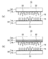
液晶表示装置における液晶配向制御用突起の設置箇所について図19を用いて説明する。図19は、液晶配向制御用突起を用いた液晶表示装置を示す概略図である。図19(a)において、液晶表示装置10は、ガラス基板12と、導電層14と、液晶分子15を含む液晶層16と、導電層18と、ガラス基板20とをこの順で積層した構造を有している。図19(a)において液晶配向制御用突起22は、導電層14と液晶層16との間、及び、導電層18と液晶層16との間に設けることができる。また、図19(b)に示すように、液晶表示装置10が、導電層18とガラス基板20との間にカラーフィルター24を有する場合も同様に、液晶配向制御用突起22は、図19(b)に示すように導電層18と液晶層16との間、及び、導電層14と液晶層16との間に設けることができる。尚、液晶配向制御用突起22と液晶層16との間には、液晶配向膜(ポリイミド膜)が設けられていてもよい。
Locations of the liquid crystal alignment control protrusions in the liquid crystal display device will be described with reference to FIG. FIG. 19 is a schematic view showing a liquid crystal display device using liquid crystal alignment control protrusions. 19A, the liquid
以下、本発明に用いる感光性転写材料、並びに、これを用いて形成した液晶配向制御用突起及び液晶表示装置について詳細に説明する。 Hereinafter, the photosensitive transfer material used in the present invention, and the liquid crystal alignment control protrusion and the liquid crystal display device formed using the same will be described in detail.
《感光性転写材料》
本発明に用いる感光性転写材料は、少なくとも1層の感光性樹脂層を有し、必要に応じて、熱可塑性樹脂層と、中間層とを有することができる。以下、仮支持体上に熱可塑性樹脂層、中間層及び感光性樹脂層をこの順で積層した態様を例に、本発明に用いる感光性転写材料について説明する。但し、本発明はこれに限定されるものではなく、仮支持体上に直接感光性樹脂層が形成された態様であってもよいし、仮支持体と感光性樹脂層との間に、熱可塑性樹脂層及び中間層のいずれかのみが形成された態様であってもよい。
<Photosensitive transfer material>
The photosensitive transfer material used in the present invention has at least one photosensitive resin layer, and may have a thermoplastic resin layer and an intermediate layer as necessary. Hereinafter, the photosensitive transfer material used in the present invention will be described taking an example in which a thermoplastic resin layer, an intermediate layer, and a photosensitive resin layer are laminated in this order on a temporary support. However, the present invention is not limited to this, and may be an embodiment in which a photosensitive resin layer is formed directly on the temporary support, or between the temporary support and the photosensitive resin layer. Only one of the plastic resin layer and the intermediate layer may be formed.
<感光性樹脂層>
上記感光性樹脂層は、クレゾール樹脂、フェノール樹脂を含有することが好ましく、更に、必要に応じてナフトキノンジアジドエステルを含むことが好ましく、更には、可塑剤や残存溶媒として高沸点溶媒、その他の添加剤を含むことができる。フェノール・ノボラック樹脂等については、公知の樹脂でよく、特開平6−308722号公報、特開平8−272091号公報、特開平6−14888号公報、特開平6−194827号公報記載のものを挙げることができる。
<Photosensitive resin layer>
The photosensitive resin layer preferably contains a cresol resin and a phenol resin, and further preferably contains a naphthoquinone diazide ester as necessary. Further, a high-boiling solvent as a plasticizer and a residual solvent, and other additions An agent can be included. The phenol novolac resin and the like may be known resins, and examples thereof include those described in JP-A-6-308722, JP-A-8-272091, JP-A-6-14888, and JP-A-6-194727. be able to.
(クレゾール樹脂)
上記クレゾール樹脂としては、クレゾールに対するホルムアルデヒドのモル比が0.7〜1.0程度のものが好ましく、0.8〜1.0が更に好ましい。また、上記クレゾール樹脂の質量平均分子量としては、800〜8000が好ましく、1000〜6000が特に好ましい。
(Cresol resin)
The cresol resin preferably has a molar ratio of formaldehyde to cresol of about 0.7 to 1.0, more preferably 0.8 to 1.0. Moreover, as a mass average molecular weight of the said cresol resin, 800-8000 are preferable and 1000-6000 are especially preferable.
上記クレゾール樹脂の異性体比(o−体/m−体/p−体のモル比率)は特に限定はないが、現像性を高める観点から全異性体に対するp−体の比率が10モル%以上であることが好ましく、20モル%以上であることが更に好ましい。また、液晶パネル性能(焼き付け防止能など)を高める観点からは、m−体の比率が5モル%以上であることが好ましく、20モル%以上であることが好ましい。 The isomer ratio (molar ratio of o-isomer / m-isomer / p-isomer) of the cresol resin is not particularly limited, but the ratio of p-isomer to all isomers is 10 mol% or more from the viewpoint of improving developability. It is preferable that it is 20 mol% or more. Further, from the viewpoint of improving the liquid crystal panel performance (such as anti-seizing ability), the m-isomer ratio is preferably 5 mol% or more, and preferably 20 mol% or more.
上記クレゾール樹脂は、単独で用いてもよいし、2種以上の混合物として用いることもできる。この場合、フェノール樹脂等の他の樹脂と混合して用いてもよい。また、本発明においては、上記クレゾール樹脂として、ナフトキノンジアジドスルホン酸エステルとの反応生成物等のクレゾール樹脂の誘導体を用いてもよい。 The said cresol resin may be used independently and can also be used as a 2 or more types of mixture. In this case, you may mix and use other resin, such as a phenol resin. In the present invention, a cresol resin derivative such as a reaction product with naphthoquinone diazide sulfonate may be used as the cresol resin.
上記クレゾール樹脂の使用量としては、0.1〜10g/m2が好ましく、0.5〜5g/m2がさらに好ましい。 The amount of the cresol resin used is preferably 0.1 to 10 g / m @ 2, more preferably 0.5 to 5 g / m @ 2.
(ナフトキノンジアジドエステル)
上記感光性樹脂層には、ナフトキノンジアジドエステルをクレゾール樹脂と併用することが好ましい。上記ナフトキノンジアジドエステルは、1官能の化合物であってもよいし2官能以上の化合物であってもよく、更にこれらの混合物であってもよい。1官能のナフトキノンジアジドエステルとしては、ナフトキノン−4−スルホン酸クロリド若しくはナフトキノン−5−スルホン酸クロリドと、置換フェノールとを反応させたエステル化合物であることが好ましい。
(Naphthoquinone diazide ester)
It is preferable to use naphthoquinone diazide ester together with a cresol resin in the photosensitive resin layer. The naphthoquinone diazide ester may be a monofunctional compound, a bifunctional or higher compound, and a mixture thereof. The monofunctional naphthoquinone diazide ester is preferably an ester compound obtained by reacting naphthoquinone-4-sulfonic acid chloride or naphthoquinone-5-sulfonic acid chloride with a substituted phenol.
また、2官能以上のナフトキノンジアジドエステルとしては、ナフトキノン−4−スルホン酸クロリド若しくはナフトキノン−5−スルホン酸クロリドと、フェノール性水酸基を複数有する化合物とを反応させたエステル化合物であることが好ましい。上記フェノール性水酸基を複数有する化合物としては、例えば、ビスフェノール類、トリスフェノール類、テトラキノスフェノール類等のポリフェノール類;ジヒドロキシベンゼン、トリヒドロキシベンゼン等の多官能フェノール;ビス型又はトリス型のジヒドロキシベンゼン若しくはトリヒドロキシベンゼン、非対称の多核フェノール、並びに、これらの混合物等が好ましい。 The bifunctional or higher naphthoquinone diazide ester is preferably an ester compound obtained by reacting naphthoquinone-4-sulfonic acid chloride or naphthoquinone-5-sulfonic acid chloride with a compound having a plurality of phenolic hydroxyl groups. Examples of the compound having a plurality of phenolic hydroxyl groups include polyphenols such as bisphenols, trisphenols and tetraquinosphenols; polyfunctional phenols such as dihydroxybenzene and trihydroxybenzene; bis-type or tris-type dihydroxybenzene or Trihydroxybenzene, asymmetric polynuclear phenol, a mixture thereof, and the like are preferable.
上記フェノール性水酸基を有する化合物の具体例としては、例えば、4−t−ブチルフェノール、4−イソアミルフェノール、4−t−オクチルフェノール、2−イソプロピル−5−メチルフェノール、2−アセチルフェノール、4−ヒドロキシベンゾフェノン、3−クロロフェノール、4−ベンジルオキシカルボニルフェノール、4−ドデシルフェノール、レゾルシノール、4−(1−メチル−1−フェニルエチル)−1,3−ベンゼンジオール、フロログルシノール、4,4'−ジヒドロキシベンゾフェノン、ビス(4−ヒドロキシフェニル)メタン、1,1−ビス(4−ヒドロキシフェニル)シクロヘキサン、2,2−ビス(3−メチル−4−ヒドロキシフェニル)メタン、2,3,4,4'−テトラヒドロキシベンゾフェノン、4,4'−[(4−ヒドロキシフェニル)メチレン]ビス[2−シクロヘキシル−5−メチルフェノール]等が挙げられる。 Specific examples of the compound having a phenolic hydroxyl group include, for example, 4-t-butylphenol, 4-isoamylphenol, 4-t-octylphenol, 2-isopropyl-5-methylphenol, 2-acetylphenol, and 4-hydroxybenzophenone. , 3-chlorophenol, 4-benzyloxycarbonylphenol, 4-dodecylphenol, resorcinol, 4- (1-methyl-1-phenylethyl) -1,3-benzenediol, phloroglucinol, 4,4′-dihydroxy Benzophenone, bis (4-hydroxyphenyl) methane, 1,1-bis (4-hydroxyphenyl) cyclohexane, 2,2-bis (3-methyl-4-hydroxyphenyl) methane, 2,3,4,4′- Tetrahydroxybenzophenone, 4,4 ' [(4-hydroxyphenyl) methylene] bis [2-cyclohexyl-5-methylphenol], and the like.
上記ナフトキノンジアジドエステルの具体例としては、例えば、4'−t−オクチルフェニルナフトキノンジアジド−4−スルホネート、4'−t−オクチルフェニルナフトキノンジアジド−5−スルホネート、4'−ベンゾイルフェニルナフトキノンジアジド−5−スルホネート、2,3,4−トリヒドロキシベンゾフェノンと1,2−ナフトキノンジアジド−5−スルホン酸クロリドとの反応物、2,3,4,4'−テトラヒドロキシベンゾフェノンと1,2−ナフトキノンジアジド−5−スルホン酸クロリドとの反応物が挙げられる。これらは単独で用いてもよいし、2種以上を併用してもよい。 Specific examples of the naphthoquinonediazide ester include, for example, 4′-t-octylphenylnaphthoquinonediazide-4-sulfonate, 4′-t-octylphenylnaphthoquinonediazide-5-sulfonate, 4′-benzoylphenylnaphthoquinonediazide-5 Sulfonate, reaction product of 2,3,4-trihydroxybenzophenone and 1,2-naphthoquinonediazide-5-sulfonic acid chloride, 2,3,4,4′-tetrahydroxybenzophenone and 1,2-naphthoquinonediazide-5 -Reaction products with sulfonic acid chloride. These may be used alone or in combination of two or more.
上記感光性樹脂中のナフトキノンジアジドエステルのクレゾール樹脂に対する質量比は、現像性を高める観点から1〜200質量%が好ましく、5〜50質量%が更に好ましい。 The mass ratio of the naphthoquinone diazide ester to the cresol resin in the photosensitive resin is preferably 1 to 200% by mass and more preferably 5 to 50% by mass from the viewpoint of improving developability.
(その他の添加剤)
上記感光性樹脂層には、感光性樹脂層の現像性を促進させるために、2価以上の脂肪族カルボン酸や、2〜6価のフェノール化合物を含有していてもよい。上記2価以上の脂肪族カルボン酸としては、例えば、マロン酸、コハク酸、フマル酸、マレイン酸、ヒドロキシコハク酸、グルタル酸、アジピン酸等が挙げられ、マロン酸、コハク酸が好ましい。上記感光性樹脂中の全固形分に対する上記2価以上の脂肪族カルボン酸の含有量としては、0.5〜20質量%が好ましく、5〜15質量%が更に好ましい。
(Other additives)
In order to promote the developability of the photosensitive resin layer, the photosensitive resin layer may contain a divalent or higher aliphatic carboxylic acid or a divalent to hexavalent phenol compound. Examples of the divalent or higher aliphatic carboxylic acid include malonic acid, succinic acid, fumaric acid, maleic acid, hydroxysuccinic acid, glutaric acid, and adipic acid, and malonic acid and succinic acid are preferable. As content of the said bivalent or more aliphatic carboxylic acid with respect to the total solid in the said photosensitive resin, 0.5-20 mass% is preferable, and 5-15 mass% is still more preferable.
また、上記2〜6価のフェノール化合物としては、2〜4価のフェノール化合物が特に好ましい。上記2〜6価のフェノール化合物としては、例えば、レゾルシノール、4−(1−メチル−1−フェニルエチル)−1,3−ベンゼンジオール、フロログルシノール、4,4'−ジヒドロキシベンゾフェノン、ビス(4−ヒドロキシフェニル)メタン、1,1−ビス(4−ヒドロキシフェニル)シクロヘキサン、2,2−ビス(3−メチル−4−ヒドロキシフェニル)メタン、2,3,4,4'−テトラヒドロキシベンゾフェノン、4,4'−[(4−ヒドロキシフェニル)メチレン]ビス[2−シクロヘキシル−5−メチルフェノール]等が挙げられ、レゾルシノール、1,1−ビス(4−ヒドロキシフェニル)シクロヘキサンが好ましい。上記感光性樹脂中の全固形分に対する上記2〜6価のフェノール化合物の含有量としては、0.5〜20質量%が好ましく、5〜15質量%が更に好ましい。 Moreover, as said 2-6 valent phenol compound, a 2-4 valent phenol compound is especially preferable. Examples of the divalent to hexavalent phenol compound include resorcinol, 4- (1-methyl-1-phenylethyl) -1,3-benzenediol, phloroglucinol, 4,4′-dihydroxybenzophenone, bis (4 -Hydroxyphenyl) methane, 1,1-bis (4-hydroxyphenyl) cyclohexane, 2,2-bis (3-methyl-4-hydroxyphenyl) methane, 2,3,4,4'-tetrahydroxybenzophenone, 4 , 4 ′-[(4-hydroxyphenyl) methylene] bis [2-cyclohexyl-5-methylphenol] and the like, and resorcinol and 1,1-bis (4-hydroxyphenyl) cyclohexane are preferable. As content of the said 2-6 valent phenol compound with respect to the total solid in the said photosensitive resin, 0.5-20 mass% is preferable, and 5-15 mass% is still more preferable.
更に、上記感光性樹脂層には、液晶配向制御用突起の形成時における転写不良や精度不良等の故障の認識を可能とし、製造適性を向上させる観点から、消色性染料を添加することもできる。上記消色性染料とは、一般に、200℃、1時間の加熱により消色し得る色素を意味し、ベーク時に消色可能な有色染料である。上記消色性染料としては、180℃、1時間の加熱により消色する色素が好ましい。このような色素は、通常、熱による分解若しくは酸化等による構造変化を起こすか、或いは熱によって蒸発若しくは昇華するものである。また、消色性染料を用いて液晶配向制御用突起を作製した場合、該液晶配向制御用突起は、消色後に、400〜800nmの平行光線に対して90%以上の光透過率を有することが好ましい。 Furthermore, a decolorizable dye may be added to the photosensitive resin layer from the viewpoint of enabling recognition of failures such as transfer failure and accuracy failure during the formation of the liquid crystal alignment control protrusions and improving manufacturing suitability. it can. The decolorizable dye generally means a pigment that can be decolored by heating at 200 ° C. for 1 hour, and is a colored dye that can be decolored during baking. As the decolorizable dye, a dye that can be decolored by heating at 180 ° C. for 1 hour is preferable. Such dyes usually undergo structural changes due to thermal decomposition or oxidation, or are evaporated or sublimated by heat. In addition, when a liquid crystal alignment control protrusion is produced using a decolorizable dye, the liquid crystal alignment control protrusion has a light transmittance of 90% or more with respect to parallel light of 400 to 800 nm after decoloring. Is preferred.
上記消色性染料としては、熱によって分解する色素として、例えば、ビクトリアピュアブルーBOH、ビクトリアピュアブルーBOH−M、マラカイトグリーン、アイゼンマラカイトグリーン、マラカイトグリーン塩酸塩、アイゼンダイヤモンドグリーン等のジアルキルアミノトリフェニルメタン系の染料等が挙げられる。また、熱により蒸発又は昇華する色素としては、例えば、オリエントオイルブラウン、メチルイエロー、スミカロンブリリアントブルーB、1,3,5−トリフェニルテトラゾリウムホルマザンなどが挙げられる。 Examples of the decolorizable dye include dyes that decompose by heat, such as dialkylaminotriphenyl such as Victoria Pure Blue BOH, Victoria Pure Blue BOH-M, Malachite Green, Eisen Malachite Green, Malachite Green Hydrochloride, Eisen Diamond Green, and the like. Examples include methane-based dyes. Examples of the dye that evaporates or sublimates by heat include Orient Oil Brown, Methyl Yellow, Sumicaron Brilliant Blue B, 1,3,5-triphenyltetrazolium formazan, and the like.
上記消色性染料としては、上記のほか、染料便覧(有機合成化学協会編、丸善、昭和47年7月20日発行)に記載される、昇華堅牢試験の耐汚染性の評価(180℃、1時間以下の条件)が1〜3のものも使用可能である。具体的には、C.I. Disperse Yellow 8, 31, 72、C.I. Disperse Orange 1, 3,20, 21 、C.I. Disperse Red 15, 55, 60, 65、C.I.Disperse Violet 8, 23,26, 37、C.I. Disperse Blue 20, 26, 55, 56, 72, 90, 91, 92, 106、C.I. Disperse Black 29、 Diacellition Direct Black B M/D (三菱化成(株)製)、Sumikaron Violet RS (住友化学(株)製)、Dianix Fast Sky Blue B M/D(三菱化成(株)製)、Miketon Polyester Blue BCL, GRN (三井石油化学(株)製)、KayaronPolyester Navy Blue GF(日本化薬(株)製)等が挙げられる。加熱装置の適性、環境汚染を考慮すると、前記消色性染料としては、熱分解性の染料が好ましい。
As the decolorizable dye, in addition to the above, the stain resistance evaluation of the sublimation fastness test described in Dye Handbook (edited by Synthetic Organic Chemistry Association, Maruzen, issued July 20, 1972) (180 ° C., Those having a condition of 1 to 3 hours) can also be used. Specifically, CI Disperse Yellow 8, 31, 72, CI Disperse
前記消色性染料の添加量としては、感光性樹脂層の全固形分に対して0.1〜10質量%であることが好ましい。 The addition amount of the decolorizable dye is preferably 0.1 to 10% by mass with respect to the total solid content of the photosensitive resin layer.
また、上記感光性樹脂層には、熱可塑性の結合剤を用いることができる。上記熱可塑性の結合剤としては、例えば、エチレン性不飽和化合物等の公知の結合剤が挙げられる。上記結合剤及び可塑剤の添加量は、本発明の効果を損なわない範囲で適宜決定される。 Moreover, a thermoplastic binder can be used for the photosensitive resin layer. Examples of the thermoplastic binder include known binders such as ethylenically unsaturated compounds. The addition amount of the binder and the plasticizer is appropriately determined as long as the effects of the present invention are not impaired.
(感光性樹脂層)
本発明の感光性転写材料は、感光性樹脂層にクレゾール樹脂とナフトキノンジアジドエステルとを併用することで、所望のパターンで露光した際に該露光部をアルカリ水溶液等による現像によって除去するポジ型の感光性転写材料とすることができる。即ち、アルカリ可溶性のクレゾール樹脂に対し、ナフトキノンジアジドエステルは溶解禁止剤として作用するが、光を受けるとインデンカルボン酸を生成し、溶解禁止効果がなくなる。このため、クレゾール樹脂とナフトキノンジアジドとを含む、上記感光性樹脂層は、アルカリ現像により光照射部のみが溶解されるポジ型レジストとして機能する。
(Photosensitive resin layer)
The photosensitive transfer material of the present invention is a positive transfer material that uses a cresol resin and a naphthoquinone diazide ester in combination with a photosensitive resin layer to remove the exposed portion by development with an aqueous alkaline solution when exposed in a desired pattern. It can be a photosensitive transfer material. That is, naphthoquinone diazide ester acts as a dissolution inhibitor for alkali-soluble cresol resins, but when it receives light, it produces indenecarboxylic acid and the dissolution-inhibiting effect is lost. For this reason, the said photosensitive resin layer containing a cresol resin and a naphthoquinone diazide functions as a positive resist in which only a light irradiation part is melt | dissolved by alkali image development.
上記感光性樹脂層の層厚としては、0.5〜10μmが好ましく、1〜6μmが更に好ましい。上記膜厚が0.5〜10μmの範囲内にあると、感光性樹脂層用塗布液を仮支持体上に塗布する際に、ピンホールが発生しにくく、現像持に露光部の除去を容易におこなうことができる。 The layer thickness of the photosensitive resin layer is preferably 0.5 to 10 μm, and more preferably 1 to 6 μm. When the film thickness is in the range of 0.5 to 10 μm, when the photosensitive resin layer coating solution is applied onto the temporary support, pinholes are unlikely to occur, and the exposed portion can be easily removed for development. Can be done.
上記感光性樹脂層は、上述のクレゾール樹脂やナフトキノンジアジドエステル等の感光性樹脂層に含まれる成分を溶剤に溶解した感光性樹脂組成物を、仮支持体(仮支持体と感光性樹脂層との間に熱可塑性樹脂層や中間層が設けられている場合にはその層)上に、種々の塗布手段を用いて塗布、乾燥することで形成することができる。 The photosensitive resin layer comprises a photosensitive resin composition in which components contained in the photosensitive resin layer such as the cresol resin and naphthoquinonediazide ester described above are dissolved in a solvent, a temporary support (a temporary support and a photosensitive resin layer, and In the case where a thermoplastic resin layer or an intermediate layer is provided between the layers, it can be formed by applying and drying on the layer) using various application means.
上記感光性樹脂組成物に用いられる溶剤としては、本発明の効果を損なわない範囲で公知の溶剤から適宜選定したものを用いることができる。上記溶剤としては、例えば、メタノール、エタノール等のアルコール類;テトラヒドロフラン等のエーテル類;エチレングリコールモノメチルエーテル、エチレングリコールジメチルエーテル、エチレングリコールメチルエチルエーテル、エチレングリコールモノエチルエーテル等のグリコールエーテル類;メチルセロソルブアセテート、エチルセロソルブアセテート等のエチレングリコールアルキルエーテルアセテート類;ジエチレングリコールモノメチルエーテル、ジエチレングリコールジエチルエーテル、ジエチレングリコールジメチルエーテル、ジエチレングリコールエチルメチルエーテル、ジエチレングリコールモノエチルエーテル、ジエチレングリコールモノブチルエーテル等のジエチレングリコール類;プロピレングリコールメチルエーテルアセテート、プロピレングリコールエチルエーテルアセテート等のプロピレングリコールアルキルエーテルアセテート類;トルエン、キシレン等の芳香族炭化水素類;アセトン、メチルエチルケトン、シクロヘキサノン、4−ヒドロキシ−4−メチル−2−ペンタノン等のケトン類;2−ヒドロキシプロピオン酸エチル、2−ヒドロキシ−2−メチルプロピオン酸メチル、2−ヒドロキシ−2−メチルプロピオン酸エチル、エトキシ酢酸エチル、ヒドロキシ酢酸エチル、2−ヒドロキシ−2−メチルブタン酸メチル、3−メトキシプロピオン酸メチル、3−メトキンプロピオン酸エチル、3−エトキシプロピオン酸メチル、3−エトキシプロピオン酸エチル、酢酸エチル、酢酸ブチル等のエステル類;等が挙げられる。これらの有機溶剤は、一種を単独で用いてもよいし、二種以上を組合わせて用いてもよい。 As a solvent used for the said photosensitive resin composition, what was selected from the well-known solvent suitably can be used in the range which does not impair the effect of this invention. Examples of the solvent include alcohols such as methanol and ethanol; ethers such as tetrahydrofuran; glycol ethers such as ethylene glycol monomethyl ether, ethylene glycol dimethyl ether, ethylene glycol methyl ethyl ether, and ethylene glycol monoethyl ether; methyl cellosolve acetate Ethylene glycol alkyl ether acetates such as ethyl cellosolve acetate; diethylene glycols such as diethylene glycol monomethyl ether, diethylene glycol diethyl ether, diethylene glycol dimethyl ether, diethylene glycol ethyl methyl ether, diethylene glycol monoethyl ether, and diethylene glycol monobutyl ether; propylene glycol Propylene glycol alkyl ether acetates such as tilether acetate and propylene glycol ethyl ether acetate; Aromatic hydrocarbons such as toluene and xylene; Ketones such as acetone, methyl ethyl ketone, cyclohexanone and 4-hydroxy-4-methyl-2-pentanone Ethyl 2-hydroxypropionate, methyl 2-hydroxy-2-methylpropionate, ethyl 2-hydroxy-2-methylpropionate, ethyl ethoxyacetate, ethyl hydroxyacetate, methyl 2-hydroxy-2-methylbutanoate, 3- And esters such as methyl methoxypropionate, ethyl 3-methoquinpropionate, methyl 3-ethoxypropionate, ethyl 3-ethoxypropionate, ethyl acetate, butyl acetate; and the like. These organic solvents may be used individually by 1 type, and may be used in combination of 2 or more type.
これらの中でも、各成分の溶解性、及び膜形成性の点で、メチルエチルケトン等のケトン類、エチレングリコールジメチルエーテル等のグリコールエーテル類、エチルセロソルブアセテート等のエチレングリコールアルキルエーテルアセテート類、2−ヒドロキシプロピオン酸エチル、3−メトキシプロピオン酸メチル、3−エトキシプロピオン酸エチル等のエステル類、ジエチレングリコールジメチルエーテル等のジエチレングリコール類が特に好適である。 Among these, in terms of solubility of each component and film forming property, ketones such as methyl ethyl ketone, glycol ethers such as ethylene glycol dimethyl ether, ethylene glycol alkyl ether acetates such as ethyl cellosolve acetate, 2-hydroxypropionic acid Particularly suitable are esters such as ethyl, methyl 3-methoxypropionate and ethyl 3-ethoxypropionate, and diethylene glycols such as diethylene glycol dimethyl ether.
上記感光性樹脂層を形成するための上記塗布手段としては、公知の塗布手段を適宜選定することができる。 As the coating means for forming the photosensitive resin layer, a known coating means can be appropriately selected.
<仮支持体>
上記仮支持体としては、後述する熱可塑性樹脂層に対して、転写の支障とならない程度の剥離性を有するものが好ましく、化学的、熱的に安定で可撓性のものが好ましい。上記仮支持体としては、具体的に、テフロン(登録商標)、ポリエチレンテレフタレート、ポリカーボネート、ポリエチレン、ポリプロピレン等の薄膜シート若しくはこれらの積層物が好適に挙げられる。
<Temporary support>
As the temporary support, those having a releasability that does not interfere with transfer with respect to a thermoplastic resin layer described later are preferable, and those that are chemically and thermally stable and flexible are preferable. Specific examples of the temporary support include a thin film sheet such as Teflon (registered trademark), polyethylene terephthalate, polycarbonate, polyethylene, and polypropylene, or a laminate thereof.
上記仮支持体と熱可塑性樹脂層との間には、良好な剥離性を確保するために、グロー放電等の表面処理は施さず、またゼラチン等の下塗り層も設けないことが好ましい。上記仮支持体の厚みとしては、5〜300μmが適当であり、20〜150μmが好ましい。 Between the temporary support and the thermoplastic resin layer, it is preferable that surface treatment such as glow discharge is not performed and an undercoat layer such as gelatin is not provided in order to ensure good peelability. As thickness of the said temporary support body, 5-300 micrometers is suitable and 20-150 micrometers is preferable.
上記感光性樹脂層の酸素透過速度は大きいことが好ましい。感光性樹脂層の酸素透過速度を大きくするには、結晶性が低くガラス転移温度が低い樹脂を用いることが望ましく、樹脂を可塑化する添加剤を加えてもよい。 It is preferable that the photosensitive resin layer has a high oxygen transmission rate. In order to increase the oxygen transmission rate of the photosensitive resin layer, it is desirable to use a resin having low crystallinity and a low glass transition temperature, and an additive for plasticizing the resin may be added.
<熱可塑性樹脂層>
熱可塑性樹脂層は、仮支持体上の第一層目として設けられ、主として熱可塑性樹脂を含んでなり、必要に応じて他の成分を含んでいてもよい。上記熱可塑性樹脂としては、転写後のアルカリ現像を可能とし、或いは転写時の転写条件によっては熱可塑性樹脂が周囲にはみ出して被転写体である基板上を汚染してしまう場合に除去処理を可能とするために、アルカリ性水溶液に可溶な樹脂が好適である。更に、熱可塑性樹脂層は、被転写体である基板上(又はカラーフィルタ上)に転写する際、基板上(又はカラーフィルタ上)に存在する凸部に起因して生じうる転写不良を防止するクッション材としての機能をも発揮させる観点から、加熱密着時に被転写物表面の凸部に応じて変形しうる性質を有することが好ましい。
<Thermoplastic resin layer>
The thermoplastic resin layer is provided as the first layer on the temporary support and mainly contains a thermoplastic resin, and may contain other components as necessary. As the above-mentioned thermoplastic resin, alkali development after transfer is possible, or removal processing is possible when the thermoplastic resin protrudes to the surroundings and contaminates the substrate to be transferred depending on the transfer conditions at the time of transfer. Therefore, a resin that is soluble in an alkaline aqueous solution is preferable. Furthermore, the thermoplastic resin layer prevents transfer defects that may occur due to convex portions existing on the substrate (or on the color filter) when transferring onto the substrate (or on the color filter) that is the transfer target. From the viewpoint of also exerting the function as a cushioning material, it is preferable that it has a property that it can be deformed according to the convex portion of the surface of the transfer object during heat adhesion.
上記の点から、上記熱可塑性樹脂としては、アルカリ可溶性であって、実質的な軟化点が80℃以下の樹脂が好ましい。軟化点が80℃以下の熱可塑性樹脂としては、例えば、エチレンとアクリル酸エステル共重合体とのケン化物、スチレンと(メタ)アクリル酸エステル共重合体とのケン化物、ビニルトルエンと(メタ)アクリル酸エステル共重合体とのケン化物、ポリ(メタ)アクリル酸エステル、(メタ)アクリル酸ブチルと酢酸ビニル等との(メタ)アクリル酸エステル共重合体等のケン化物等が挙げられる。上記熱可塑性樹脂は、一種単独からなるものであっても、二種以上を併用したものであってもよい。 In view of the above, the thermoplastic resin is preferably an alkali-soluble resin having a substantial softening point of 80 ° C. or lower. Examples of thermoplastic resins having a softening point of 80 ° C. or lower include saponified products of ethylene and acrylate copolymers, saponified products of styrene and (meth) acrylate copolymers, vinyltoluene and (meth). Examples include saponified products such as saponified products with acrylic acid ester copolymers, poly (meth) acrylic acid esters, and (meth) acrylic acid ester copolymers of butyl (meth) acrylate and vinyl acetate. The thermoplastic resin may be a single type or a combination of two or more types.
更に、上記熱可塑性樹脂としては、「プラスチック性能便覧」(日本プラスチック工業連盟、全日本プラスチック成形工業連合会編著、工業調査会発行、1968年10月25日発行)に記載の、軟化点が約80℃以下の有機高分子物質のうち、アルカリ水溶液に可溶なものも使用できる。 Further, the thermoplastic resin has a softening point of about 80 as described in “Plastic Performance Handbook” (edited by the Japan Plastics Industry Federation, edited by the All Japan Plastics Molding Industry Association, published by the Industrial Research Council, issued on October 25, 1968). Among organic polymer substances having a temperature of 0 ° C. or lower, those soluble in an alkaline aqueous solution can be used.
また、軟化点80℃以上の有機高分子物質であっても、その有機高分子物質中に該有機高分子物質と相溶性のある各種公知の可塑剤を添加することにより、実質的な軟化点を80℃以下に下げて使用することもできる。 In addition, even when an organic polymer substance has a softening point of 80 ° C. or higher, a substantial softening point can be obtained by adding various known plasticizers compatible with the organic polymer substance to the organic polymer substance. The temperature can be lowered to 80 ° C. or lower.
上記有機高分子物質を用いる場合、上述の仮支持体との接着力を調節する目的で、実質的な軟化点が80℃を超えない範囲で、各種ポリマー、過冷却物質、密着改良剤、界面活性剤、離型剤等を加えることもできる。 When the organic polymer substance is used, various polymers, supercooling substances, adhesion improvers, interfaces, and the like within a range where the substantial softening point does not exceed 80 ° C. for the purpose of adjusting the adhesive force with the temporary support described above. An activator, a release agent and the like can also be added.
本発明の感光性転写材料は、仮支持体上に熱可塑性樹脂層の他、後述の中間層、及び上記感光性樹脂層を順次積層して構成することができるが、特に熱可塑性樹脂層と仮支持体との間の接着強度が他の層間における接着強度よりも小さくすることが必要である。これにより転写の後、仮支持体を容易に剥離することができ、更に剥離の際に熱可塑性樹脂層表面の破壊を伴うことなく仮支持体を除去することができる。これは、仮支持体除去後の感光性樹脂層への露光を均一に行うことが可能となる点で好ましい態様である。 The photosensitive transfer material of the present invention can be formed by sequentially laminating a later-described intermediate layer and the photosensitive resin layer on the temporary support, in addition to the thermoplastic resin layer. It is necessary that the adhesive strength between the temporary support and the adhesive strength between other layers be smaller. Thereby, after transfer, the temporary support can be easily peeled off, and further, the temporary support can be removed without being accompanied by destruction of the surface of the thermoplastic resin layer. This is a preferable aspect in that the exposure to the photosensitive resin layer after removing the temporary support can be performed uniformly.
上記熱可塑性樹脂層は、熱可塑性樹脂と必要に応じて他の成分とを有機溶剤に溶解して塗布液(熱可塑性樹脂層用塗布液)を調製し、例えば、スピンコート法等の公知の塗布方法で塗布等して形成することが可能である。 The thermoplastic resin layer is prepared by dissolving a thermoplastic resin and other components as required in an organic solvent to prepare a coating solution (a coating solution for a thermoplastic resin layer). It can be formed by coating or the like by a coating method.
上記有機溶剤としては、例えば、メタノール、エタノール等のアルコール類;テトラヒドロフラン等のエーテル類;エチレングリコールモノメチルエーテル、エチレングリコールジメチルエーテル、エチレングリコールメチルエチルエーテル、エチレングリコールモノエチルエーテル等のグリコールエーテル類;メチルセロソルブアセテート、エチルセロソルブアセテート等のエチレングリコールアルキルエーテルアセテート類;ジエチレングリコールモノメチルエーテル、ジエチレングリコールジエチルエーテル、ジエチレングリコールジメチルエーテル、ジエチレングリコールエチルメチルエーテル、ジエチレングリコールモノエチルエーテル、ジエチレングリコールモノブチルエーテル等のジエチレングリコール類;プロピレングリコールメチルエーテルアセテート、プロピレングリコールエチルエーテルアセテート等のプロピレングリコールアルキルエーテルアセテート類;トルエン、キシレン等の芳香族炭化水素類;アセトン、メチルエチルケトン、シクロヘキサノン、4−ヒドロキシ−4−メチル−2−ペンタノン等のケトン類;2−ヒドロキシプロピオン酸エチル、2−ヒドロキシ−2−メチルプロピオン酸メチル、2−ヒドロキシ−2−メチルプロピオン酸エチル、エトキシ酢酸エチル、ヒドロキシ酢酸エチル、2−ヒドロキシ−2−メチルブタン酸メチル、3−メトキシプロピオン酸メチル、3−メトキンプロピオン酸エチル、3−エトキシプロピオン酸メチル、3−エトキシプロピオン酸エチル、酢酸エチル、酢酸ブチル等のエステル類;等が挙げられる。これらの有機溶剤は、一種を単独で用いてもよいし、二種以上を組合わせて用いてもよい。 Examples of the organic solvent include alcohols such as methanol and ethanol; ethers such as tetrahydrofuran; glycol ethers such as ethylene glycol monomethyl ether, ethylene glycol dimethyl ether, ethylene glycol methyl ethyl ether, and ethylene glycol monoethyl ether; methyl cellosolve Ethylene glycol alkyl ether acetates such as acetate and ethyl cellosolve acetate; diethylene glycols such as diethylene glycol monomethyl ether, diethylene glycol diethyl ether, diethylene glycol dimethyl ether, diethylene glycol ethyl methyl ether, diethylene glycol monoethyl ether, and diethylene glycol monobutyl ether; propylene glycol Propylene glycol alkyl ether acetates such as rumethyl ether acetate and propylene glycol ethyl ether acetate; Aromatic hydrocarbons such as toluene and xylene; Ketones such as acetone, methyl ethyl ketone, cyclohexanone and 4-hydroxy-4-methyl-2-pentanone Class: ethyl 2-hydroxypropionate, methyl 2-hydroxy-2-methylpropionate, ethyl 2-hydroxy-2-methylpropionate, ethyl ethoxyacetate, ethyl hydroxyacetate, methyl 2-hydroxy-2-methylbutanoate, 3 -Esters such as methyl methoxypropionate, ethyl 3-methopropionate, methyl 3-ethoxypropionate, ethyl 3-ethoxypropionate, ethyl acetate, butyl acetate; and the like. These organic solvents may be used individually by 1 type, and may be used in combination of 2 or more type.
これらの中でも、各成分の溶解性、及び膜形成性の点で、メチルエチルケトン等のケトン類、エチレングリコールジメチルエーテル等のグリコールエーテル類、エチルセロソルブアセテート等のエチレングリコールアルキルエーテルアセテート類、2−ヒドロキシプロピオン酸エチル、3−メトキシプロピオン酸メチル、3−エトキシプロピオン酸エチル等のエステル類、ジエチレングリコールジメチルエーテル等のジエチレングリコール類が特に好適である。 Among these, in terms of solubility of each component and film forming property, ketones such as methyl ethyl ketone, glycol ethers such as ethylene glycol dimethyl ether, ethylene glycol alkyl ether acetates such as ethyl cellosolve acetate, 2-hydroxypropionic acid Particularly suitable are esters such as ethyl, methyl 3-methoxypropionate and ethyl 3-ethoxypropionate, and diethylene glycols such as diethylene glycol dimethyl ether.
更に、N−メチルホルムアミド、N,N−ジメチルホルムアミド、N−メチルホルムアニリド、N−メチルアセトアミド、N,N−ジメチルアセトアミド、N−メチルピロリドン、ジメチルスルホキシド、ベンジルエチルエーテル、ジヘキシルエーテル、アセトニルアセトン、イソホロン、カプロン酸、カプリル酸、1−オクタノール、1−ノナノール、ベンジルアルコール、酢酸ベンジル、安息香酸エチル、シュウ酸ジエチル、マレイン酸ジエチル、γ−ブチロラクトン、炭酸エチレン、炭酸プロピレン、フェニルセロソルブアセテート等の高沸点溶剤を添加することもできる。 Further, N-methylformamide, N, N-dimethylformamide, N-methylformanilide, N-methylacetamide, N, N-dimethylacetamide, N-methylpyrrolidone, dimethylsulfoxide, benzylethyl ether, dihexyl ether, acetonylacetone , Isophorone, caproic acid, caprylic acid, 1-octanol, 1-nonanol, benzyl alcohol, benzyl acetate, ethyl benzoate, diethyl oxalate, diethyl maleate, γ-butyrolactone, ethylene carbonate, propylene carbonate, phenyl cellosolve acetate, etc. A high boiling point solvent can also be added.
上記熱可塑性樹脂層の層厚としては、6〜100μmが好ましく、6〜50μmがより好ましい。上記層厚が、6〜100μmの範囲内にあると、基板(又はカラーフィルタ)上の1μm以上の凸部を完全に吸収することができると共に、現像性、製造適性を向上させることができる。 As a layer thickness of the said thermoplastic resin layer, 6-100 micrometers is preferable and 6-50 micrometers is more preferable. When the layer thickness is in the range of 6 to 100 μm, convex portions of 1 μm or more on the substrate (or color filter) can be completely absorbed, and developability and production suitability can be improved.
<中間層>
上記感光性樹脂層や上記熱可塑性樹脂層には有機溶剤が用いられることから、両記中間層は、両層が互いに混ざり合うのを防止する機能を有する。また、上記中間層は、水又はアルカリ水溶液に分散又は溶解するものであればよい。
<Intermediate layer>
Since an organic solvent is used for the photosensitive resin layer and the thermoplastic resin layer, both intermediate layers have a function of preventing the two layers from being mixed with each other. Moreover, the said intermediate | middle layer should just be disperse | distributed or melt | dissolved in water or aqueous alkali solution.
上記中間層は、水又はアルカリ水溶液に分散、溶解可能な樹脂成分を主に構成され、必要に応じて、界面活性剤等の他の成分を含んでいてもよい。上記中間層を構成する樹脂成分としては、公知のものの中から適宜選択でき、例えば、特開昭46−2121号公報や特公昭56−40824号公報に記載の、ポリビニルエーテル/無水マレイン酸重合体、カルボキシアルキルセルロースの水溶性塩、水溶性セルロースエーテル類、カルボキシアルキル澱粉の水溶性塩、ポリビニルアルコール、ポリビニルピロリドン、各種のポリアクリルアミド類、各種水溶性ポリアミド、ポリアクリル酸の水溶性塩、ゼラチン、エチレンオキサイド重合体、各種澱粉及びその類似物からなる群の水溶性塩、スチレン/マレイン酸の共重合体、マレイネート樹脂、及びこれらを2種以上組合せたもの等が挙げられる。 The intermediate layer is mainly composed of a resin component that can be dispersed and dissolved in water or an aqueous alkali solution, and may contain other components such as a surfactant, if necessary. The resin component constituting the intermediate layer can be appropriately selected from known ones. For example, the polyvinyl ether / maleic anhydride polymer described in JP-A No. 46-2121 and JP-B No. 56-40824 is disclosed. , Water-soluble salts of carboxyalkyl cellulose, water-soluble cellulose ethers, water-soluble salts of carboxyalkyl starch, polyvinyl alcohol, polyvinyl pyrrolidone, various polyacrylamides, various water-soluble polyamides, water-soluble salts of polyacrylic acid, gelatin, Examples thereof include ethylene oxide polymers, water-soluble salts of the group consisting of various starches and the like, styrene / maleic acid copolymers, maleate resins, and combinations of two or more thereof.
中でも、ポリビニルアルコールとポリビニルピロリドンとを組合せてなるものが特に好ましく、更に添加剤を加えてもよい。更に、上記ポリビニルアルコールとしては、鹸化率が99%以下であるのものが好ましく、90%以下であるものが特に好ましい。また、上記ポリビニルピロリドンの含有量としては、中間層の固形分の1〜75質量%であることが好ましく、1〜60質量%であることが更に好ましく、10〜50質量%であることが最も好ましい。上記ポリビニルピロリドンの含有量が、1〜75質量%の範囲内にあると、感光性樹脂層との密着性を十分に高めることができる。
添加剤としては、用いる樹脂成分を可塑化するものが好ましく、グリセリン、エチレングリコール、プロピレングリコール、ポリエチレングリコール、ポリプロピレングリコール、及びそれらのモノエーテル体、ジエーテル体、モノエステル体、ジエステル体、モノアミド体、ジアミド体、などが挙げられる。添加剤の添加量としては、樹脂の0〜30質量%であることが好ましく、1〜20質量%であることがさらに好ましい。
Among these, a combination of polyvinyl alcohol and polyvinyl pyrrolidone is particularly preferable, and an additive may be further added. Further, the polyvinyl alcohol preferably has a saponification rate of 99% or less, particularly preferably 90% or less. Moreover, as content of the said polyvinylpyrrolidone, it is preferable that it is 1-75 mass% of solid content of an intermediate | middle layer, It is more preferable that it is 1-60 mass%, It is most 10-50 mass% preferable. Adhesiveness with the photosensitive resin layer can be sufficiently enhanced when the content of the polyvinyl pyrrolidone is in the range of 1 to 75% by mass.
As the additive, those that plasticize the resin component to be used are preferable, glycerin, ethylene glycol, propylene glycol, polyethylene glycol, polypropylene glycol, and their monoether, diether, monoester, diester, monoamide, And diamide compounds. The addition amount of the additive is preferably 0 to 30% by mass of the resin, and more preferably 1 to 20% by mass.
上記中間層は、樹脂成分等を水系溶媒に溶解、分散して塗布液(中間層用塗布液)を調製し、該塗布液を上記熱可塑性樹脂層上に公知の塗布方法により塗布して形成することが可能である。
上記水系溶媒としては、蒸留水等の水を主成分とし、所望により本発明の効果を損なわない範囲でアルコール等の水と親和性のある溶剤や塩等を添加した溶媒が挙げられる。
The intermediate layer is formed by dissolving and dispersing a resin component or the like in an aqueous solvent to prepare a coating liquid (intermediate layer coating liquid) and coating the coating liquid on the thermoplastic resin layer by a known coating method. Is possible.
Examples of the aqueous solvent include a solvent containing water such as distilled water as a main component and, if desired, a solvent having affinity with water such as alcohol, a salt, or the like as long as the effects of the present invention are not impaired.
上記中間層の層厚としては、約0.1〜5μmが好ましく、0.5〜2μmがより好ましい。上記層厚が、0.1から5μmの間にあると、熱可塑性樹脂層と感光性樹脂層の層混合を起こすことがなく、現像や中間層除去を容易に行うことができる。 The thickness of the intermediate layer is preferably about 0.1 to 5 μm, and more preferably 0.5 to 2 μm. When the layer thickness is between 0.1 and 5 μm, layer mixing of the thermoplastic resin layer and the photosensitive resin layer does not occur, and development and intermediate layer removal can be easily performed.
<表面保護フィルム>
上記感光性樹脂層上には、保管等の際の汚れや損傷から保護する目的で、表面保護フィルムを設ける。上記表面保護フィルムは、感光性樹脂層に容易に貼付可能で、また、感光性樹脂層から容易に剥離可能なものの中から選択でき、上記仮支持体と同一又は類似の材料からなるものであってもよい。具体的には、シリコーン紙、ポリオレフィン又はポリテトラフルオロエチレンシート等が好ましく、中でも、ポリエチレン、ポリプロピレンフィルムがより好ましい。さらに、表面保護フィルムの感光性樹脂層と接する面に深さ0.3μm以上の凹部が1cm2あたり1000個以上あることが好ましく、深さ0.3μm以上の凹部が1cm2あたり5000個以上あることがより好ましい。該凹部は、フィルムのエンボス加工により形成されても良いし、マット化処理(サンドブラスト法)により形成されていても良く、さらにエッチング処理により凹凸をなめらかにしても良い。これらは特開平1−110930記載の方法などにより作製することができる。表面保護フィルム表面の凹部の数は光学顕微鏡で観察することにより計測できる。
また、表面保護フィルム表面の凹部の深さとは、中心面平均高さから各凹部の最深部までの距離のことであり、まず中心面平均高さをもとめた後に、各凹部の最深部までの距離を測ることによりもとめられ、具体的にはレーザー顕微鏡、表面粗さ形状測定機(サーフコム;東京精密(株)製)などにより計測できる。
<Surface protection film>
A surface protective film is provided on the photosensitive resin layer for the purpose of protecting it from dirt and damage during storage. The surface protective film can be easily affixed to the photosensitive resin layer, and can be selected from those easily peelable from the photosensitive resin layer, and is made of the same or similar material as the temporary support. May be. Specifically, silicone paper, polyolefin, polytetrafluoroethylene sheet or the like is preferable, and among them, polyethylene and polypropylene films are more preferable. Furthermore, it is preferable that there are 1000 or more recesses with a depth of 0.3 μm or more per
In addition, the depth of the concave portion on the surface protective film surface is the distance from the center plane average height to the deepest portion of each concave portion, and after first obtaining the central plane average height, the depth to the deepest portion of each concave portion It can be determined by measuring the distance. Specifically, it can be measured by a laser microscope, a surface roughness shape measuring machine (Surfcom; manufactured by Tokyo Seimitsu Co., Ltd.), or the like.
上記表面保護フィルムの厚みとしては、約5〜100μmが好ましく、10〜60μmがより好ましい。 As thickness of the said surface protection film, about 5-100 micrometers is preferable and 10-60 micrometers is more preferable.
<感光性転写材料の製造方法>
本発明に用いる感光性転写材料は、上記仮支持体上に、まず、熱可塑性樹脂を溶剤に溶解し調製した塗布液(熱可塑性樹脂層用塗布液)を塗布・乾燥して、熱可塑性樹脂層を設け、続いて該熱可塑性樹脂層上に、熱可塑性樹脂層を溶解しない溶媒を用いてなる塗布液(中間層用塗布液)を塗布、乾燥して中間層を設け、更に該中間層上に、中間層を溶解しない溶剤にクレゾール樹脂等を溶解し調製した塗布液(感光性樹脂層用塗布液)を塗布、乾燥して感光性樹脂層を設けることにより形成することができる。或いは、上記表面保護フィルム上に感光性樹脂層を設けると共に、別途仮支持体上に熱可塑性樹脂層と中間層とを設け、それぞれを中間層と感光性樹脂層とが接するように貼り合わせることにより形成することもできる。また、本発明に用いる感光性転写材料は、上記表面保護フィルム上に感光性樹脂層と中間層とを設けると共に、別途仮支持体上に熱可塑性樹脂層を設け、それぞれを上述と同様に、中間層と感光性樹脂層とが接するように貼り合わせることによって、製造することができる。
<Method for producing photosensitive transfer material>
The photosensitive transfer material used in the present invention is obtained by first applying a coating solution (a coating solution for a thermoplastic resin layer) prepared by dissolving a thermoplastic resin in a solvent onto the temporary support, and drying the thermoplastic resin. Next, a coating solution (intermediate layer coating solution) using a solvent that does not dissolve the thermoplastic resin layer is applied on the thermoplastic resin layer, and dried to provide an intermediate layer. It can be formed by applying a coating solution prepared by dissolving cresol resin or the like in a solvent that does not dissolve the intermediate layer (photosensitive resin layer coating solution) and drying to provide a photosensitive resin layer. Alternatively, a photosensitive resin layer is provided on the surface protective film, and a thermoplastic resin layer and an intermediate layer are separately provided on a temporary support, and the intermediate layer and the photosensitive resin layer are bonded to each other. Can also be formed. In addition, the photosensitive transfer material used in the present invention is provided with a photosensitive resin layer and an intermediate layer on the surface protective film, and separately provided with a thermoplastic resin layer on a temporary support, respectively, It can manufacture by bonding together so that an intermediate | middle layer and the photosensitive resin layer may contact | connect.
また、後述するように、本発明に用いる感光性転写材料を被転写体である基板やカラーフィルタ上に密着させた後、感光性転写材料の仮支持体を剥離する過程では、仮支持体や基板等が帯電する結果、周囲のゴミ等を引き寄せ、剥離後の感光性樹脂層上にゴミ等が付着することがある。このような場合、その後の露光過程で感光性樹脂層に未露光部ができ、その部分が現像の際に残ってしまうことがある。このため、帯電を防止する目的で、仮支持体の少なくとも一方の表面に導電性層を設けたり、或いは導電性を付与した仮支持体を用いることによって、その表面の電気抵抗を1013Ω以下にまで低下させることが好ましい。 Further, as described later, after the photosensitive transfer material used in the present invention is adhered to a substrate or a color filter which is a transfer target, in the process of peeling the temporary support of the photosensitive transfer material, As a result of the substrate and the like being charged, the surrounding dust or the like may be attracted, and the dust or the like may adhere to the photosensitive resin layer after peeling. In such a case, an unexposed portion may be formed in the photosensitive resin layer in the subsequent exposure process, and the portion may remain during development. For this reason, for the purpose of preventing electrification, by providing a conductive layer on at least one surface of the temporary support or using a temporary support with conductivity, the electrical resistance of the surface is reduced to 1013 Ω or less. It is preferable to reduce.
上述のように仮支持体に導電性を付与するためには、仮支持体中に導電性物質を含有させればよい。このような方法としては、例えば、金属酸化物の微粒子や帯電防止剤を予め練り込んでおく方法が好適である。上記金属酸化物としては、酸化亜鉛、酸化チタン、酸化錫、酸化アルミニウム、酸化インジウム、酸化珪素、酸化マグネシウム、酸化バリウム、酸化モリブデン等の結晶性金属酸化物、及び/又は、その複合酸化物の微粒子が挙げられる。 In order to impart conductivity to the temporary support as described above, a conductive substance may be contained in the temporary support. As such a method, for example, a method of kneading metal oxide fine particles or an antistatic agent in advance is suitable. Examples of the metal oxide include zinc oxide, titanium oxide, tin oxide, aluminum oxide, indium oxide, silicon oxide, magnesium oxide, barium oxide, and crystalline oxides such as molybdenum oxide and / or composite oxides thereof. Fine particles are mentioned.
上記帯電防止剤としては、エレクトロストリッパーA(花王(株)製)、エレノンNo.19(第一工業製薬(株)製)等のアルキル燐酸塩系アニオン界面活性剤;アモーゲンK(第一工業製薬(株)製)等のベタイン系両性界面活性剤;ニッサンノニオンL(日本油脂(株)製)等のポリオキシエチレン脂肪酸エステル系非イオン界面活性剤;エマルゲン106、120、147、420、220、905、910(花王(株)製)やニッサンノニオンE(日本油脂(株)製)等のポリオキシエチレンアルキルエーテル系非イオン界面活性剤、等が好適である。その他、非イオン界面活性剤として、ポリオキシエチレンアルキルフェノールエーテル系、多価アルコール脂肪酸エステル系、ポリオキシエチレンソルビタン脂肪酸エステル系、ポリオキシエチレンアルキルアミン系等のものが挙げられる。 Examples of the antistatic agent include Electro Stripper A (manufactured by Kao Corporation), Elenon No. Alkyl phosphate anionic surfactants such as 19 (Daiichi Kogyo Seiyaku Co., Ltd.); Betaine amphoteric surfactants such as Amorgen K (Daiichi Kogyo Seiyaku Co., Ltd.); Nissan Nonion L (Nippon Yushi Polyoxyethylene fatty acid ester-based nonionic surfactants such as Emulgen 106, 120, 147, 420, 220, 905, 910 (made by Kao Corporation) and Nissan Nonion E (made by Nippon Oil & Fats Co., Ltd.) Polyoxyethylene alkyl ether type nonionic surfactants such as) are suitable. Other nonionic surfactants include polyoxyethylene alkylphenol ethers, polyhydric alcohol fatty acid esters, polyoxyethylene sorbitan fatty acid esters, polyoxyethylene alkylamines, and the like.
仮支持体上に導電性層を設ける場合、該導電性層は公知のものの中から、適宜選択して用いることができる。上記導電性層に用いる導電性物質として、ZnO、TiO2、SnO2、Al2O3、In2O3、SiO2、MgO、BaO、MoO3等から選ばれる少なくとも1種の結晶性金属酸化物、及び/又は、その複合酸化物の微粒子等が挙げられる。これらの導電性物質を導電性層に含有させて用いる方法が湿度環境に影響されず、安定した導電効果を発揮する点で好ましい。 When the conductive layer is provided on the temporary support, the conductive layer can be appropriately selected from known ones. As the conductive material used for the conductive layer, at least one crystalline metal oxide selected from ZnO, TiO2, SnO2, Al2O3, In2O3, SiO2, MgO, BaO, MoO3, and / or a composite oxide thereof Fine particles. A method in which these conductive substances are contained in a conductive layer and used is preferable in that a stable conductive effect is exhibited without being affected by the humidity environment.
また、上記結晶性金属酸化物又はその複合酸化物の微粒子の体積抵抗値としては、107Ω・cm以下が好ましく、105Ω・cm以下が更に好ましい。また、その粒子径としては、0.01〜0.7μmが好ましく、0.02〜0.5μmが更に好ましい。 The volume resistance value of the crystalline metal oxide or the composite oxide fine particles is preferably 10 7 Ω · cm or less, more preferably 10 5 Ω · cm or less. Moreover, as the particle diameter, 0.01-0.7 micrometer is preferable and 0.02-0.5 micrometer is still more preferable.
上記結晶性金属酸化物及びその複合酸化物の微粒子の製造方法は、特開昭56−143430号公報等に詳細に記載されている。即ち、第1に、金属酸化物微粒子を焼成によって作製し、導電性を向上させる異種原子の存在下で熱処理する方法、第2に、焼成によって金属酸化物微粒子を作製する際に導電性を向上させるための異種原子を共存させる方法、第3に、焼成により金属微粒子を作製する際に雰囲気中の酸素濃度を下げて、酸素欠陥を導入する方法等が記載されている。上記異種原子を含む具体例としては、ZnOに対してはAl、In等;TiO2に対してはNb、Ta等;、SnO2に対してはSb、Nb、ハロゲン元素等を存在させることが挙げられる。
A method for producing fine particles of the crystalline metal oxide and its composite oxide is described in detail in JP-A-56-143430. That is, firstly, metal oxide fine particles are produced by firing and heat treatment is performed in the presence of different atoms to improve conductivity, and secondly, the conductivity is improved when producing metal oxide fine particles by firing. And a third method for introducing oxygen defects by reducing the oxygen concentration in the atmosphere when producing metal fine particles by firing. Specific examples of the hetero atom include Al, In, etc. for ZnO; Nb, Ta, etc. for
上記異種原子の添加量としては、0.01〜30mol%が好ましく、0.1〜10mol%がより好ましい。導電性粒子の使用量としては、0.05〜20g/m2が好ましく、0.1〜10g/m2がより好ましい。 As addition amount of the said different atom, 0.01-30 mol% is preferable and 0.1-10 mol% is more preferable. The amount of conductive particles used is preferably 0.05 to 20 g / m @ 2, more preferably 0.1 to 10 g / m @ 2.
本発明の感光性転写材料の仮支持体に設けられる導電性層には、バインダーとして、例えば、ゼラチン、セルロースナイトレート、セルローストリアセテート、セルロースジアセテート、セルロースアセテートブチレート、セルロースアセテートプロピオネート等のセルロースエステル;塩化ビニリデン、塩化ビニル、スチレン、アクリロニトリル、酢酸ビニル、炭素数1〜4のアルキルアクリレート、ビニルピロリドン等を含むホモポリマー又は共重合体;可溶性ポリエステル、ポリカーボネート、可溶性ポリアミド等を使用することができる。 In the conductive layer provided on the temporary support of the photosensitive transfer material of the present invention, as a binder, for example, gelatin, cellulose nitrate, cellulose triacetate, cellulose diacetate, cellulose acetate butyrate, cellulose acetate propionate, etc. Cellulose esters; homopolymers or copolymers containing vinylidene chloride, vinyl chloride, styrene, acrylonitrile, vinyl acetate, alkyl acrylates having 1 to 4 carbon atoms, vinyl pyrrolidone, etc .; soluble polyesters, polycarbonates, soluble polyamides, etc. may be used it can.
また、これらのバインダー中に導電性粒子を分散する場合、チタン系分散剤又はシラン系分散剤等の分散液を添加してもよく、更に、必要に応じてバインダー架橋剤等を添加することもできる。 In addition, when dispersing conductive particles in these binders, a dispersion such as a titanium-based dispersant or a silane-based dispersant may be added, and a binder cross-linking agent may be added as necessary. it can.
上記チタン系分散剤としては、例えば、米国特許第4,069,192号公報、同第4,080,353号公報等に記載の、チタネート系カップリング剤、プレンアクト(味の素(株)製)などが挙げられる。上記シラン系分散剤としては、例えば、ビニルトリクロルシラン、ビニルトリエトキシシラン、ビニルトリス(β−メトキシエトキシ)シラン、γ−グリシドキシプロピルトリメトキシシラン、γ−メタクリロキシプロピルトリメトキシシラン等が挙げられ、「シランカップリング剤」(信越化学工業(株)製)として市販されている。上記バインダー架橋剤としては、例えば、エポキシ系架橋剤、イソシアネート系架橋剤、アジリジン系架橋剤、エポキシ系架橋剤などが挙げられる。 Examples of the titanium dispersant include titanate coupling agents, preneact (manufactured by Ajinomoto Co., Inc.) and the like described in US Pat. Nos. 4,069,192 and 4,080,353. Is mentioned. Examples of the silane dispersant include vinyltrichlorosilane, vinyltriethoxysilane, vinyltris (β-methoxyethoxy) silane, γ-glycidoxypropyltrimethoxysilane, and γ-methacryloxypropyltrimethoxysilane. "Silane coupling agent" (manufactured by Shin-Etsu Chemical Co., Ltd.). Examples of the binder crosslinking agent include an epoxy crosslinking agent, an isocyanate crosslinking agent, an aziridine crosslinking agent, and an epoxy crosslinking agent.
上記導電性層は、導電性微粒子をバインダー中に分散させて仮支持体上に塗設したり、仮支持体上に下引処理(例えば、下塗り層等)を施した上に導電性微粒子を付着
させたりすることにより設けることができる。
The conductive layer is prepared by dispersing conductive fine particles in a binder and coating the temporary support or applying a subbing treatment (for example, an undercoat layer) on the temporary support. It can be provided by attaching.
上記導電性層は、仮支持体の感光性樹脂層を塗設した面とは反対の表面上に設けてもよく、この場合には、十分な耐傷性を確保する目的で、導電性層上に更に疎水性重合体層を設けることが好ましい。この疎水性重合体層は、疎水性重合体を有機溶剤に溶解した状態又は水性ラテックスの状態で塗布すればよく、その塗布量としては、乾燥質量で0.05〜1g/m2程度が好ましい。 The conductive layer may be provided on the surface of the temporary support opposite to the surface on which the photosensitive resin layer is coated. In this case, the conductive layer is formed on the conductive layer for the purpose of ensuring sufficient scratch resistance. It is preferable to further provide a hydrophobic polymer layer. The hydrophobic polymer layer may be applied in a state where the hydrophobic polymer is dissolved in an organic solvent or in the form of an aqueous latex, and the coating amount is preferably about 0.05 to 1 g / m @ 2 in terms of dry mass.
上記疎水性重合体としては、例えば、ニトロセルロース、セルロースアセテート等のセルロースエステル;塩化ビニル、塩化ビニリデン、ビニルアクリレート等を含むビニル系ポリマー;有機溶剤可溶性ポリアミド、ポリエステル等のポリマーを挙げることができる。 Examples of the hydrophobic polymer include cellulose esters such as nitrocellulose and cellulose acetate; vinyl polymers containing vinyl chloride, vinylidene chloride, vinyl acrylate and the like; polymers such as organic solvent-soluble polyamide and polyester.
上記疎水性重合体層には、スベリ性を付与する目的で、例えば、特開昭55−79435号公報に記載の有機カルボン酸アミド等のスベリ剤を使用することができる。また、必要に応じて、マット剤等を使用することもできる。このような疎水性重合体層を設けても、導電性層の効果は実質的に影響を受けない。 For the purpose of imparting smoothness to the hydrophobic polymer layer, for example, a smoothing agent such as an organic carboxylic acid amide described in JP-A-55-79435 can be used. Moreover, a mat agent etc. can also be used as needed. Even if such a hydrophobic polymer layer is provided, the effect of the conductive layer is not substantially affected.
また、下塗り層を設ける場合、特開昭51−135526号公報、米国特許第3,143,421号公報、同第3,586,508号公報、同第2,698,235号公報、同第3,567,452号公報等に記載の塩化ビニリデン系共重合体、特開昭51−114120号公報、米国特許第3,615,556号公報等に記載のブタジエン等のジオレフイン系共重合体、特開昭51−58469号公報等に記載のグリシジルアクリレート又はグリシジルメタアクリレート含有共重合体、特開昭48−24923号公報等に記載のポリアミド・エピクロルヒドリン樹脂、特開昭50−39536号公報に記載の無水マレイン酸含有共重合体等を用いることができる。 When an undercoat layer is provided, JP-A-51-135526, U.S. Pat. Nos. 3,143,421, 3,586,508, 2,698,235, No. 3,567,452 etc., vinylidene chloride copolymer described in JP-A No. 51-114120, US Pat. No. 3,615,556 etc. Glycidyl acrylate or glycidyl methacrylate-containing copolymers described in JP-A-51-58469, polyamide / epichlorohydrin resins described in JP-A-48-24923, and JP-A-50-39536 A maleic anhydride-containing copolymer can be used.
本発明においては、特開昭56−82504号公報、特開昭56−143443号公報、特開昭57−104931号公報、特開昭57−118242号公報、特開昭58−62647号公報、特開昭60−258541号公報等に記載の導電性層も必要に応じて用いることができる。 In the present invention, JP-A-56-82504, JP-A-56-143443, JP-A-57-104931, JP-A-57-118242, JP-A-58-62647, A conductive layer described in JP-A-60-258541 can be used as necessary.
仮支持体上に、導電性層を塗布する場合、ローラーコート、エアナイフコート、グラビアコート、バーコート、カーテンコート等の公知の方法により塗布することができる。十分な帯電防止効果を得るためには、導電性層又は導電性を付与した仮支持体の表面電気抵抗値を、1013Ω以下とすることが好ましく、1012Ω以下とすることが更に好ましい。 When the conductive layer is applied on the temporary support, it can be applied by a known method such as roller coating, air knife coating, gravure coating, bar coating, or curtain coating. In order to obtain a sufficient antistatic effect, the surface electrical resistance value of the conductive layer or the temporary support provided with conductivity is preferably 10 13 Ω or less, and more preferably 10 12 Ω or less. .
また、熱可塑性樹脂層と仮支持体との強固な接着を防止するため、仮支持体面に公知の微粒子を含有する滑り剤組成物、シリコーン化合物を含有する離型剤組成物等を塗布することもできる。 In addition, in order to prevent strong adhesion between the thermoplastic resin layer and the temporary support, a slip agent composition containing known fine particles, a release agent composition containing a silicone compound, etc. are applied to the temporary support surface. You can also.
仮支持体の熱可塑性樹脂層を設けない側の表面に導電性層を設ける場合には、熱可塑性樹脂層と仮支持体との接着性を向上させる目的で、仮支持体に、例えば、グロー放電処理、コロナ処理、紫外線照射処理等の表面処理、フェノール性物質、ポリ塩化ビニリデン樹脂、スチレンブタジエンゴム、ゼラチン等の下塗り処理又はこれらの処理を組み合わせた処理を施すことができる。 When a conductive layer is provided on the surface of the temporary support on which the thermoplastic resin layer is not provided, the temporary support is provided with, for example, a glow layer for the purpose of improving the adhesion between the thermoplastic resin layer and the temporary support. Surface treatment such as discharge treatment, corona treatment, ultraviolet irradiation treatment, undercoating treatment such as phenolic substance, polyvinylidene chloride resin, styrene butadiene rubber, gelatin, or a combination of these treatments can be applied.
仮支持体用のフィルムは押し出し成形により形成することが可能であるが、導電性物質又は導電性層を仮支持体と同一又は異質のプラスチック原料に含有させ、上記フィルムと同時に押し出し成形した場合には、接着性、耐傷性に優れた導電性層を容易に得ることができる。この場合、上記疎水性重合体層や下塗り層を設ける必要はなく、転写材料を構成する導電性付与仮支持体として最も好ましい実施形態である。 The film for the temporary support can be formed by extrusion, but when a conductive material or a conductive layer is contained in the same or different plastic raw material as the temporary support and is extruded simultaneously with the film. Can easily obtain a conductive layer excellent in adhesion and scratch resistance. In this case, it is not necessary to provide the hydrophobic polymer layer or the undercoat layer, and this is the most preferred embodiment as a conductivity-imparting temporary support constituting the transfer material.
<感光性転写材料を用いたパターン形成方法>
続いて、本発明のパターン形成方法について説明する。ここでは、本発明に用いる感光性転写材料として、仮支持体上にアルカリ可溶な熱可塑性樹脂層、中間層、感光性樹脂層及び表面保護フィルムがこの順に積層されてなる感光性転写材料を用い、更に、基体上の全面にカラーフィルタ層が設けられた基板を用いた一例を示す。
<Pattern formation method using photosensitive transfer material>
Then, the pattern formation method of this invention is demonstrated. Here, as a photosensitive transfer material used in the present invention, a photosensitive transfer material in which an alkali-soluble thermoplastic resin layer, an intermediate layer, a photosensitive resin layer, and a surface protective film are laminated in this order on a temporary support. Furthermore, an example using a substrate provided with a color filter layer on the entire surface of the substrate is shown.
まず、本発明に用いる感光性転写材料の表面保護フィルムを取り除き、感光性樹脂層を加圧、加熱下で被転写体である基板上に密接し貼り合わせる。基板と感熱記録層との貼り合わせには、従来公知のラミネーター、真空ラミネーター等の中から適宜選択したものが使用でき、より生産性を高めるには、オートカットラミネーターも使用可能である。 First, the surface protective film of the photosensitive transfer material used in the present invention is removed, and the photosensitive resin layer is intimately bonded onto a substrate as a transfer target under pressure and heating. For the bonding of the substrate and the heat-sensitive recording layer, one appropriately selected from conventionally known laminators, vacuum laminators and the like can be used, and an auto-cut laminator can also be used in order to increase productivity.
この際、本発明のパターン形成方法では少なくとも一層のナフトキノンジアジド誘導体を含む感光性転写材料をラミネートすることが好ましい。感光性転写材料をラミネートする方法には、ラミネートする前にあらかじめ基板を加熱しておく方法や、ラミネート時のラミネーターのロール温度を上げる方法や、ラミネート時のラミネーターを通過するときの基板の搬送速度を遅くする方法、などがある。
ラミネートする前にあらかじめ基板を加熱しておく方法では、基板温度を80℃以上180℃以下とすることが好ましく、100℃以上130℃以下とすることがより好ましい。基板を加熱するには、ホットプレートなどの接触型の加熱器を基板に接触させて用いることもできるし、また非接触で用いることもできる。また温風加熱器、IRヒーターなどの非接触型の加熱器を非接触で用いることもできる。基板温度が120℃未満であるとパターン形成後に画素の欠けを生じることがあり、基板温度が180℃を超えると感光性転写材料中の素材が分解し、感度変化、着色などを起こすことがある。
ラミネート時のラミネーターのロール温度を上げる方法では、そのロール温度を80℃以上160℃以下とすることが好ましく、80℃以上130℃以下とすることがより好ましい。ロール温度が80℃未満であるとパターン形成後に画素の欠けを生じることがあるし、ロール温度が160℃を超えると感光性転写材料中の素材が分解し、感度変化、着色などを起こしたり、転写材料と基板間にシワを生じたりすることがある。
At this time, in the pattern forming method of the present invention, it is preferable to laminate a photosensitive transfer material containing at least one naphthoquinonediazide derivative. The method of laminating the photosensitive transfer material includes heating the substrate in advance before laminating, increasing the roll temperature of the laminator during lamination, and the substrate transport speed when passing through the laminator during lamination. There are ways to slow down.
In the method of heating the substrate in advance before laminating, the substrate temperature is preferably 80 ° C. or higher and 180 ° C. or lower, and more preferably 100 ° C. or higher and 130 ° C. or lower. In order to heat the substrate, a contact heater such as a hot plate can be used in contact with the substrate, or it can be used in a non-contact manner. Further, a non-contact type heater such as a hot air heater or an IR heater can be used in a non-contact manner. If the substrate temperature is lower than 120 ° C, pixels may be chipped after pattern formation. If the substrate temperature exceeds 180 ° C, the material in the photosensitive transfer material may be decomposed, resulting in a change in sensitivity or coloring. .
In the method of raising the laminator roll temperature during lamination, the roll temperature is preferably 80 ° C. or higher and 160 ° C. or lower, and more preferably 80 ° C. or higher and 130 ° C. or lower. If the roll temperature is less than 80 ° C, pixels may be chipped after pattern formation. If the roll temperature exceeds 160 ° C, the material in the photosensitive transfer material is decomposed, causing a sensitivity change, coloring, etc. Wrinkles may occur between the transfer material and the substrate.
ラミネート時のラミネーターを通過するときの基板の搬送速度を遅くする方法では、搬送速度を1.0m/分以上10m/分以下とすることが好ましく、1.2m/分以上5m/分以下とすることがより好ましい。搬送速度を1.0m/分未満にすると性能上の不具合はないものの、生産性の低下が問題となることがあるし、10m/分を超えるとパターン形成後に画素の欠けを生じることがある。 In the method of slowing the substrate conveyance speed when passing through the laminator during lamination, the conveyance speed is preferably 1.0 m / min or more and 10 m / min or less, and 1.2 m / min or more and 5 m / min or less. It is more preferable. If the conveyance speed is less than 1.0 m / min, there is no problem in performance, but a decrease in productivity may be a problem, and if it exceeds 10 m / min, pixel missing may occur after pattern formation.
また、本発明のパターン形成方法では、感光性転写材料を基板に転写する転写工程と所望のパターンで露光する露光工程との間に、前記感光性転写材料を転写した基板を加熱する基板加熱工程を含むことが好ましい。この際の感光性転写材料はナフトキノンジアジド誘導体を含んでいても、含んでいなくてもよい。感光性転写材料を転写した基板を加熱する工程はホットプレートなどの接触型の加熱器を基板に接触させて用いることもできるし、また非接触で用いることもできる。また温風加熱器、IRヒーターなどの非接触型の加熱器を非接触で用いることもできる。この感光性転写材料を転写した基板を加熱する工程は120℃から180℃の温度範囲で、20秒から120秒の時間範囲で行うことが好ましく、120℃から150℃の温度範囲で、20秒から50秒の時間範囲で行うことがより好ましい。120℃未満、または20秒未満であるとパターン形成後に画素の欠けを生じることがあるし、180℃を超えると感光性転写材料中の素材が分解し、感度変化、着色などを起こすことがあるし、また120秒を超えると生産性の低下が問題となることがある。 Moreover, in the pattern formation method of this invention, the board | substrate heating process which heats the board | substrate which transferred the said photosensitive transfer material between the transfer process of transferring a photosensitive transfer material to a board | substrate, and the exposure process of exposing with a desired pattern. It is preferable to contain. In this case, the photosensitive transfer material may or may not contain a naphthoquinonediazide derivative. The step of heating the substrate to which the photosensitive transfer material has been transferred can be used by bringing a contact-type heater such as a hot plate into contact with the substrate, or can be used in a non-contact manner. Further, a non-contact type heater such as a hot air heater or an IR heater can be used in a non-contact manner. The step of heating the substrate to which the photosensitive transfer material has been transferred is preferably performed in a temperature range of 120 ° C. to 180 ° C. and in a time range of 20 seconds to 120 seconds, and in a temperature range of 120 ° C. to 150 ° C. for 20 seconds. It is more preferable to carry out within a time range of from 50 seconds to 50 seconds. If the temperature is less than 120 ° C. or less than 20 seconds, pixel defects may occur after pattern formation. If the temperature exceeds 180 ° C., the material in the photosensitive transfer material may be decomposed, resulting in a change in sensitivity or coloring. In addition, if it exceeds 120 seconds, a decrease in productivity may be a problem.
感光性転写材料を基板に転写した後、所望のパターンで露光する前に、仮支持体を熱可塑性樹脂層との界面で剥がし取るが、感光性転写材料を転写した基板を加熱する工程は、仮支持体を剥がし取る前に行ってもよいし、仮支持体を剥がし取った後に行ってもよい。 After transferring the photosensitive transfer material to the substrate and before exposing with a desired pattern, the temporary support is peeled off at the interface with the thermoplastic resin layer, but the step of heating the substrate to which the photosensitive transfer material has been transferred is You may carry out before peeling off a temporary support body, and you may carry out after peeling off a temporary support body.
さらに、本発明のパターン形成方法では、少なくとも一層のナフトキノンジアジド誘導体を含む感光性転写材料を基板に転写する転写工程と所望のパターンで露光する露光工程との間に、前記感光性樹脂層の熱可塑性樹脂層と中間層とを除去する工程を含むことが好ましい。前記感光性樹脂層の熱可塑性樹脂層と中間層とを除去する工程は、公知の方法により行え、熱可塑性樹脂層と中間層を溶解して感光性樹脂層を溶解しないような溶剤若しくは水性の現像液、特にアルカリ水溶液などを用いて、例えば、(a)露光後の基板自体を現像浴中に浸漬する、(b)露光後の基板にスプレー等により噴霧する等して、更に必要に応じて、溶解性を高める目的で、回転ブラシや湿潤スポンジ等で擦ったり、超音波を照射しながら行うことができる。上記アルカリ水溶液としては、アルカリ性物質の希薄水溶液が好ましく、更に水混和性のある有機溶剤を少量添加したものも好適に使用することができる。上記アルカリ性物質としては、炭酸ナトリウム、炭酸カリウム等のアルカリ金属炭酸塩類、炭酸水素ナトリウム、炭酸水素カリウム等のアルカリ金属重炭酸塩類、ケイ酸ナトリウム、ケイ酸カリウム等のアルカリ金属ケイ酸塩類、メタケイ酸ナトリウム、メタケイ酸カリウム等のアルカリ金属メタケイ酸塩類、トリエタノールアミン、ジエタノールアミン、モノエタノールアミン、燐酸三ナトリウム等が挙げられる。 Furthermore, in the pattern forming method of the present invention, the heat of the photosensitive resin layer is transferred between a transfer step of transferring a photosensitive transfer material containing at least one naphthoquinonediazide derivative to a substrate and an exposure step of exposing with a desired pattern. It is preferable to include a step of removing the plastic resin layer and the intermediate layer. The step of removing the thermoplastic resin layer and the intermediate layer of the photosensitive resin layer can be performed by a known method, and a solvent or an aqueous solution that dissolves the thermoplastic resin layer and the intermediate layer and does not dissolve the photosensitive resin layer. Using a developer, particularly an alkaline aqueous solution, for example, (a) immersing the exposed substrate itself in a developing bath, (b) spraying the exposed substrate by spraying, etc. For the purpose of enhancing the solubility, it can be carried out while rubbing with a rotating brush or a wet sponge or by irradiating ultrasonic waves. As the alkaline aqueous solution, a dilute aqueous solution of an alkaline substance is preferable, and a solution to which a small amount of a water-miscible organic solvent is added can also be suitably used. Examples of the alkaline substance include alkali metal carbonates such as sodium carbonate and potassium carbonate, alkali metal bicarbonates such as sodium hydrogen carbonate and potassium hydrogen carbonate, alkali metal silicates such as sodium silicate and potassium silicate, and metasilicic acid. Examples include alkali metal metasilicates such as sodium and potassium metasilicate, triethanolamine, diethanolamine, monoethanolamine, and trisodium phosphate.
感光性転写材料を基板に転写した後、所望のパターンで露光する前に、仮支持体を熱可塑性樹脂層との界面で剥がし取るが、感光性転写材料の熱可塑性樹脂層と中間層とを除去する工程は、仮支持体を剥がし取った後に行うのが好ましい。 After transferring the photosensitive transfer material to the substrate and before exposing with a desired pattern, the temporary support is peeled off at the interface with the thermoplastic resin layer, but the thermoplastic resin layer and the intermediate layer of the photosensitive transfer material are removed. The step of removing is preferably performed after peeling off the temporary support.
これらの、感光性転写材料をラミネートする方法、転写工程と露光工程との間に感光性転写材料を転写した基板を加熱する方法、転写工程と露光工程との間に感光性樹脂層の熱可塑性樹脂層と中間層とを除去する方法は、それぞれ単独で行ってもよいし、併せて行ってもよい。 The method of laminating the photosensitive transfer material, the method of heating the substrate having the photosensitive transfer material transferred between the transfer step and the exposure step, and the thermoplasticity of the photosensitive resin layer between the transfer step and the exposure step. The method for removing the resin layer and the intermediate layer may be performed independently or in combination.
前述のように、感光性転写材料をラミネートし、及び/または、転写工程と露光工程との間に感光性転写材料を転写した基板を加熱し、及び/または、転写工程と露光工程との間に感光性転写材料の熱可塑性樹脂層と中間層とを除去した後、熱可塑性樹脂層と中間層がある場合には、熱可塑性樹脂層の上方から熱可塑性樹脂層及び中間層を通して、また熱可塑性樹脂層と中間層がない場合には、感光性樹脂層の上方から、感光性樹脂層をポジ用の露光(パターニング)する。 As described above, the photosensitive transfer material is laminated and / or the substrate on which the photosensitive transfer material is transferred between the transfer process and the exposure process, and / or between the transfer process and the exposure process. If there is a thermoplastic resin layer and an intermediate layer after removing the thermoplastic resin layer and the intermediate layer of the photosensitive transfer material, the thermoplastic resin layer and the intermediate layer are passed through the thermoplastic resin layer and the intermediate layer from above. When there is no plastic resin layer and intermediate layer, the photosensitive resin layer is subjected to positive exposure (patterning) from above the photosensitive resin layer.
次に本発明におけるパターニングの方法において、2次元状に並んだ空間光変調デバイスを用いて、画像データに基づいて光を変調しながら相対走査することで2次元画像の形成を行う露光工程を有する。 Next, the patterning method of the present invention includes an exposure step of forming a two-dimensional image by using a spatial light modulation device arranged in two dimensions to perform relative scanning while modulating light based on image data. .
以下、この露光工程について、説明する。 Hereinafter, this exposure process will be described.
(マスクレス露光の定義)
本発明のマスクレス露光は、マスクレスパターン露光とも呼ばれることがある。露光光を透過させない、または、弱めて透過させる材質で画像(露光パターン、パターンとも言う)を形成した「マスク」と呼ばれる物体を露光光の光路に配置し、感光層を、該画像に対応したパターン状に露光する従来の露光方式(マスク露光と言う)に対し、前記の「マスク」を使用せずに感光層をパターン状に露光する露光方式の事である。
本発明のマスクレス露光は、より詳しくは、画像データに基づいて光を変調しながら相対走査する事で二次元画像の形成を行う露光ということができる。
(Definition of maskless exposure)
The maskless exposure of the present invention may also be called maskless pattern exposure. An object called a `` mask '' that forms an image (exposure pattern, also referred to as a pattern) with a material that does not transmit the exposure light or weakly transmits it is placed in the optical path of the exposure light, and the photosensitive layer corresponds to the image. This is an exposure method in which a photosensitive layer is exposed in a pattern without using the above-mentioned “mask”, compared to a conventional exposure method in which the pattern is exposed (referred to as mask exposure).
More specifically, the maskless exposure of the present invention can be referred to as exposure for forming a two-dimensional image by performing relative scanning while modulating light based on image data.
(光源の説明)
本発明のマスクレス露光では、光源として超高圧水銀灯や、レーザーが用いられる。
超高圧水銀灯とは、石英ガラスチューブなどに水銀を封入した放電灯であり水銀の蒸気圧を高く設定して発光効率を高めたものである(点灯時の水銀の蒸気圧はおよそ5MPaになるものもある W. Elenbaas : Light Sources 、Philips Technical Library 148-150)。である。輝線スペクトルのうち、i線(365nm)、h線(405nm)、g線(436nm)が、中でも365nmが主として用いられる。
(Description of light source)
In the maskless exposure of the present invention, an ultrahigh pressure mercury lamp or a laser is used as a light source.
An ultra-high pressure mercury lamp is a discharge lamp in which mercury is sealed in a quartz glass tube, etc., and has a high vapor pressure of mercury to improve luminous efficiency (the mercury vapor pressure during lighting is about 5 MPa) W. Elenbaas: Light Sources, Philips Technical Library 148-150). It is. Of the bright line spectrum, i-line (365 nm), h-line (405 nm), and g-line (436 nm) are used, with 365 nm being mainly used.
レーザー、英語のLight Amplification by Stimulated Emission of Radiation(誘導放出による光の増幅)の頭字語である。反転分布を持った物質中で起きる誘導放出の現象を利用し、光波の増幅、発振によって干渉性と指向性が一層強い単色光を作り出す発振器及び増幅器。励起媒質として結晶、ガラス、液体、色素、気体などあり、これらの媒質から固体レーザー(YAGレーザー)、液体レーザー、気体レーザー(アルゴンレーザー、He−Neレーザー、炭酸ガスレーザー、エキシマレーザー)、半導体レーザーなどの公知のレーザーを用いることができる。 Laser, an acronym for Light Amplification by Stimulated Emission of Radiation in English. Oscillators and amplifiers that produce monochromatic light with stronger coherence and directivity by amplifying and oscillating light waves, utilizing the phenomenon of stimulated emission that occurs in materials with an inverted distribution. There are crystals, glass, liquid, dye, gas, etc. as excitation media. Solid laser (YAG laser), liquid laser, gas laser (argon laser, He-Ne laser, carbon dioxide laser, excimer laser), semiconductor laser from these media A known laser such as can be used.
半導体レーザーは 搬送子の注入、電子ビームによる励起、衝突によるイオン化、光励起などによって電子と正孔とが接合部に流出する時、pn接合で可干渉光を誘導放出するような発光ダイオードを用いるレーザーである。この放出される可干渉光の波長は、半導体化合物によって決まる。
レーザーの波長は、特に限定されないが、中でも解像度とレーザー装置のコスト、入手のしやすさの観点から、半導体レーザーでは、300〜500nmの波長域から選択するのが好ましいが、340〜450nmがより好ましく、特に405nmは好ましい。
また固体レーザーでは、YAG-SHG固体レーザー の 532nmが挙げられる。更に、半導体励起固体レーザーでは 532・355・266nmが挙げられ、従来のレジスト用光重合開始剤が感度を有すという点では355nmが好ましく選ばれる。
気体レーザーでは、KrFレーザーの249nm ArFレーザーの193nmが用いられる。
これらの光源の中で、表示装置の製造工程で、感光性材料を露光する場合を考えると、露光波長が、410nmとなる光源を選択することが、表示領域の透過率を高くする観点で好ましい。
A semiconductor laser uses a light emitting diode that induces coherent light at a pn junction when electrons and holes flow out to the junction due to carrier injection, electron beam excitation, collision ionization, photoexcitation, etc. It is. The wavelength of the emitted coherent light is determined by the semiconductor compound.
The wavelength of the laser is not particularly limited. However, from the viewpoint of resolution, cost of the laser device, and availability, it is preferable to select a semiconductor laser from a wavelength range of 300 to 500 nm, but 340 to 450 nm is more preferable. 405 nm is particularly preferable.
For solid-state lasers, the YAG-SHG solid-state laser at 532 nm can be mentioned. Furthermore, 532, 355, and 266 nm can be cited for semiconductor-excited solid-state lasers, and 355 nm is preferably selected from the viewpoint that conventional photopolymerization initiators for resists have sensitivity.
In the gas laser, a KrF laser of 249 nm and an ArF laser of 193 nm are used.
Among these light sources, considering the case where the photosensitive material is exposed in the manufacturing process of the display device, it is preferable to select a light source having an exposure wavelength of 410 nm from the viewpoint of increasing the transmittance of the display region. .
本発明の光を変調しながら相対走査する方法について説明する。
そのひとつの代表的な方法は、DMD(デジタル・マイクロミラー・デバイス、例えば、1987年、米国テキサス・インスツルメンツの ラリー・ホーンベック博士他が開発した光半導体)のような、微小なミラーが二次元に並んだ空間変調素子を用いる方法である。
この場合、光源からの光は、適切な光学系によってDMD上に照射され、DMDに二次元に並んだ各ミラーからの反射光が、別の光学系などを経て、感光層上に、二次元に並んだ光点の像を形成する。このままでは光点と光点の間は露光されないが、前記二次元に並んだ光点の像を、二次元の並び方向に対して、やや傾いた方向に移動させると、最初の列の光点と光点の間を、後方の列の光点が露光する、という形で、感光層の全面を露光することができる。DMDの各ミラーの角度を制御し、前記光点をON-OFFする事で、画像パターンを形成することができる。このようなDMDを有す露光ヘッドを並べて用いることで色々な幅の基板に対応することができる。
前記DMDでは、前記光点の輝度は、ONかOFFの2階調しかないが、ミラー階調型空間変調素子を用いると、256階調の露光を行うことができる。
A method of relative scanning while modulating light according to the present invention will be described.
One typical method is a two-dimensional micromirror such as DMD (digital micromirror device, for example, an optical semiconductor developed by Dr. Larry Hornbeck et al. In 1987 in Texas Instruments). This is a method of using spatial modulation elements arranged in line.
In this case, the light from the light source is irradiated onto the DMD by an appropriate optical system, and the reflected light from each mirror arranged two-dimensionally on the DMD passes through another optical system and the like on the photosensitive layer in a two-dimensional manner. An image of light spots arranged in a row is formed. If the light spot is not exposed between the light spots, the image of the light spots arranged in two dimensions is moved in a direction slightly inclined with respect to the two-dimensional arrangement direction. The entire surface of the photosensitive layer can be exposed in such a manner that the light spots in the rear row are exposed between the light spots. An image pattern can be formed by controlling the angle of each mirror of the DMD and turning the light spot on and off. By aligning and using such exposure heads having DMD, it is possible to deal with substrates of various widths.
In the DMD, the brightness of the light spot has only two gradations, ON or OFF, but 256 gradation exposure can be performed by using a mirror gradation spatial modulation element.
一方、本発明の光を変調しながら相対走査する方法の、別の代表的な方法は、ポリゴンミラーを用いる方法である。ポリゴンミラー ( polygon mirror ) とは 周囲に一連の平面反射面を持った回転部材の事。感光層上に光源からの光を反射して照射するが、反射光の光点は、該平面鏡の回転によって走査される。この走査方向に対して直角に基板を移動させることで、基板上の感光層の全面を露光することができる。光源からの光の強度を適切な方法でON-OFFまたは、中間調に制御することで、画像パターンを形成することができる。光源からの光を複数本とすることで、走査時間を短縮することができる。 On the other hand, another representative method of relative scanning while modulating light according to the present invention is a method using a polygon mirror. A polygon mirror is a rotating member that has a series of flat reflective surfaces around it. The light from the light source is reflected and irradiated onto the photosensitive layer, and the light spot of the reflected light is scanned by the rotation of the plane mirror. By moving the substrate at right angles to the scanning direction, the entire surface of the photosensitive layer on the substrate can be exposed. An image pattern can be formed by controlling the intensity of light from the light source to ON-OFF or halftone by an appropriate method. By using a plurality of light from the light source, the scanning time can be shortened.
本発明の光を変調しながら相対走査する方法としては、例えば、以下の方法も適用することができる。
特開平5−150175に記載のポリゴンミラーを用いて描画する例、特表2004−523101(WO2002/039793)に記載の下部レイヤの画像の一部を視覚的に取得し、ポリゴンミラーを用いた装置で上部レイヤの位置を下部レイヤ位置に揃えて露光する例、特開2004−56080に記載のDMD有する露光する例、特表2002−523905に記載のポリゴンミラー備えた露光装置、特開2001−255661に記載のポリゴンミラー備えた露光装置、特開2003−50469に記載のDMD、LD、多重露光の組み合わせ例、特開2003−156853に記載の基板の部位により露光量を変える露光方法
の例、特開2005−43576に記載の位置ずれ調整を行う露光方法の例等である。
As a method of performing relative scanning while modulating light of the present invention, for example, the following method can also be applied.
An example of drawing using a polygon mirror described in Japanese Patent Laid-Open No. 5-150175, an apparatus using a polygon mirror by visually acquiring a part of an image of a lower layer described in JP-T-2004-523101 (WO2002 / 039793) In this example, exposure is performed with the position of the upper layer aligned with the position of the lower layer, an example of exposure with DMD described in JP-A-2004-56080, an exposure apparatus equipped with a polygon mirror described in JP-T-2002-523905, and JP-A-2001-255661. An exposure apparatus including a polygon mirror described in JP-A-2003-50469, an example of a combination of DMD, LD, and multiple exposure described in JP-A-2003-50469, an example of an exposure method that changes an exposure amount depending on a part of a substrate described in JP-A-2003-156893, This is an example of an exposure method for performing misalignment adjustment described in Japanese Patent Application Laid-Open No. 2005-43576.
以下、相対走査露光について詳細に説明する。
(相対走査露光)
本発明の露光方法としては超高圧水銀灯を用いる方法とレーザーを用いる方法があるが、好ましいのは後者である。
本発明で用いられるレーザーとしてはアルゴンレーザー、He−Neレーザー、半導体レーザー、炭酸ガスレーザー、YAGレーザーなどの公知のレーザーを用いることができる。
レーザーの波長は、特に限定されないが、中でも、画像パターン(例えば、配向制御用突起)の解像度とレーザー装置のコスト、入手のしやすさの観点から、300〜500nmの波長域から選択するのが好ましいが、340〜450nmがより好ましく、特に405nmは好ましい。
レーザーのビーム径は、特に限定されないが、中でも、画像パターン(例えば、配向制御用突起)の解像度の観点から、ガウシアンビームの1/e2値で5〜30μmが好ましく、7〜20μmがより好ましい。
レーザービームのエネルギー量としては、特に限定されないが、中でも、露光時間と解像度の観点から、1〜100mJ/cm2が好ましく、5〜20mJ/cm2がより好ましい。
本発明ではレーザー光を画像データに応じて空間光変調することが必要である。この目的のため空間光変調素子であるデジタル・マイクロ・デバイスを用いることが好ましい。
Hereinafter, the relative scanning exposure will be described in detail.
(Relative scanning exposure)
The exposure method of the present invention includes a method using an ultrahigh pressure mercury lamp and a method using a laser, but the latter is preferred.
As the laser used in the present invention, known lasers such as an argon laser, a He—Ne laser, a semiconductor laser, a carbon dioxide gas laser, and a YAG laser can be used.
The wavelength of the laser is not particularly limited, but in particular, it is selected from the wavelength range of 300 to 500 nm from the viewpoint of the resolution of the image pattern (for example, alignment control protrusion), the cost of the laser device, and the availability. Although preferably 340 to 450 nm, more preferably 405 nm.
The beam diameter of the laser is not particularly limited, but among them, from the viewpoint of the resolution of the image pattern (for example, alignment control protrusion), the 1 / e 2 value of the Gaussian beam is preferably 5 to 30 μm, more preferably 7 to 20 μm. .
Although it does not specifically limit as energy amount of a laser beam, From a viewpoint of exposure time and resolution, 1-100 mJ / cm < 2 > is preferable especially and 5-20 mJ / cm < 2 > is more preferable.
In the present invention, it is necessary to spatially modulate laser light according to image data. For this purpose, it is preferable to use a digital micro device which is a spatial light modulation element.
前記露光装置としては、例えば、下記の装置を用いて露光することができる。 As the exposure apparatus, for example, exposure can be performed using the following apparatus.
以下にレーザー光を用いた3次元露光装置の一例を示すが、本発明における露光装置はこれに限定されるものではない。
露光ユニットは、図1に示すように、ガラス基板150を表面に吸着して保持する平板状のステージ152を備えている。4本の脚部154に支持された厚い板状の設置台156の上面には、ステージ移動方向に沿って延びた2本のガイド158が設置されている。ステージ152は、その長手方向がステージ移動方向を向くように配置されると共に、ガイド158によって往復移動可能に支持されている。なお、この露光装置には、ステージ152をガイド158に沿って駆動するための図示しない駆動装置が設けられている。
An example of a three-dimensional exposure apparatus using laser light is shown below, but the exposure apparatus in the present invention is not limited to this.
As shown in FIG. 1, the exposure unit includes a
設置台156の中央部には、ステージ152の移動経路を跨ぐようにコ字状のゲート160が設けられている。コ字状のゲート160の端部の各々は、設置台156の両側面に固定されている。このゲート160を挟んで一方の側にはスキャナ162が設けられ、他方の側には感光材料150の先端及び後端を検知する複数(例えば、2個)の検知センサ164が設けられている。スキャナ162及び検知センサ164はゲート160に各々取り付けられて、ステージ152の移動経路の上方に固定配置されている。なお、スキャナ162及び検知センサ164は、これらを制御する図示しないコントローラに接続されている。
A
スキャナ162は、図2及び図3(B)に示すように、m行n列(例えば、3行5列)の略マトリックス状に配列された複数(例えば、14個)の露光ヘッド166を備えている。この例では、感光材料150の幅との関係で、3行目には4個の露光ヘッド166を配置した。なお、m行目のn列目に配列された個々の露光ヘッドを示す場合は、露光ヘッド166mnと表記する。
As shown in FIGS. 2 and 3B, the
露光ヘッド166による露光エリア168は、副走査方向を短辺とする矩形状である。従って、ステージ152の移動に伴い、感光材料150には露光ヘッド166毎に帯状の露光済み領域170が形成される。なお、m行目のn列目に配列された個々の露光ヘッドによる露光エリアを示す場合は、露光エリア168mnと表記する。
An
また、図3(A)及び(B)に示すように、帯状の露光済み領域170が副走査方向と直交する方向に隙間無く並ぶように、ライン状に配列された各行の露光ヘッドの各々は、配列方向に所定間隔(露光エリアの長辺の自然数倍、ここでは2倍)ずらして配置されている。このため、1行目の露光エリア16811と露光エリア16812との間の露光できない部分は、2行目の露光エリア16821と3行目の露光エリア16831とにより露光することができる。
Further, as shown in FIGS. 3A and 3B, each of the exposure heads in each row arranged in a line so that the strip-shaped exposed
露光ヘッド16611〜166mn各々は、図4、図5(A)及び(B)に示すように、入射された光ビームを画像データに応じて各画素毎に変調する空間光変調素子として、デジタル・マイクロミラー・デバイス(DMD)50を備えている。このDMD50は、データ処理部とミラー駆動制御部とを備えた図示しないコントローラに接続されている。このコントローラのデータ処理部では、入力された画像データに基づいて、各露光ヘッド166毎にDMD50の制御すべき領域内の各マイクロミラーを駆動制御する制御信号を生成する。なお、制御すべき領域については後述する。また、ミラー駆動制御部では、画像データ処理部で生成した制御信号に基づいて、各露光ヘッド166毎にDMD50の各マイクロミラーの反射面の角度を制御する。なお、反射面の角度の制御に付いては後述する。
Each of the exposure heads 166 11 to 166 mn is a spatial light modulator that modulates an incident light beam for each pixel according to image data, as shown in FIGS. 4, 5 (A) and (B). A digital micromirror device (DMD) 50 is provided. The
DMD50の光入射側には、光ファイバの出射端部(発光点)が露光エリア168の長辺方向と対応する方向に沿って一列に配列されたレーザー出射部を備えたファイバアレイ光源66、ファイバアレイ光源66から出射されたレーザ光を補正してDMD上に集光させるレンズ系67、レンズ系67を透過したレーザー光をDMD50に向けて反射するミラー69がこの順に配置されている。
On the light incident side of the
レンズ系67は、ファイバアレイ光源66から出射されたレーザー光を平行光化する1対の組合せレンズ71、平行光化されたレーザー光の光量分布が均一になるように補正する1対の組合せレンズ73、及び光量分布が補正されたレーザー光をDMD上に集光する集光レンズ75で構成されている。組合せレンズ73は、レーザー出射端の配列方向に対しては、レンズの光軸に近い部分は光束を広げ且つ光軸から離れた部分は光束を縮め、且つこの配列方向と直交する方向に対しては光をそのまま通過させる機能を備えており、光量分布が均一となるようにレーザー光を補正する。
The
また、DMD50の光反射側には、DMD50で反射されたレーザー光を感光材料150の走査面(被露光面)56上に結像するレンズ系54、58が配置されている。レンズ系54及び58は、DMD50と被露光面56とが共役な関係となるように配置されている。
Further, on the light reflection side of the
DMD50は、図6に示すように、SRAMセル(メモリセル)60上に、微小ミラー(マイクロミラー)62が支柱により支持されて配置されたものであり、画素(ピクセル)を構成する多数の(例えば、600個×800個)の微小ミラーを格子状に配列して構成されたミラーデバイスである。各ピクセルには、最上部に支柱に支えられたマイクロミラー62が設けられており、マイクロミラー62の表面にはアルミニウム等の反射率の高い材料が蒸着されている。なお、マイクロミラー62の反射率は90%以上である。また、マイクロミラー62の直下には、ヒンジ及びヨークを含む支柱を介して通常の半導体メモリの製造ラインで製造されるシリコンゲートのCMOSのSRAMセル60が配置されており、全体はモノリシック(一体型)に構成されている。
As shown in FIG. 6, the
DMD50のSRAMセル60にデジタル信号が書き込まれると、支柱に支えられたマイクロミラー62が、対角線を中心としてDMD50が配置された基板側に対して±α度(例えば±10度)の範囲で傾けられる。図7(A)は、マイクロミラー62がオン状態である+α度に傾いた状態を示し、図7(B)は、マイクロミラー62がオフ状態である−α度に傾いた状態を示す。従って、画像信号に応じて、DMD50の各ピクセルにおけるマイクロミラー62の傾きを、図6に示すように制御することによって、DMD50に入射された光はそれぞれのマイクロミラー62の傾き方向へ反射される。
When a digital signal is written in the
なお、図6には、DMD50の一部を拡大し、マイクロミラー62が+α度又は−α度に制御されている状態の一例を示す。それぞれのマイクロミラー62のオンオフ制御は、DMD50に接続された図示しないコントローラによって行われる。なお、オフ状態のマイクロミラー62により光ビームが反射される方向には、光吸収体(図示せず)が配置されている。
FIG. 6 shows an example of a state in which a part of the
また、DMD50は、その短辺が副走査方向と所定角度θ(例えば、1°〜5°)をなすように僅かに傾斜させて配置するのが好ましい。図8(A)はDMD50を傾斜させない場合の各マイクロミラーによる反射光像(露光ビーム)53の走査軌跡を示し、図8(B)はDMD50を傾斜させた場合の露光ビーム53の走査軌跡を示している。
Further, it is preferable that the
DMD50には、長手方向にマイクロミラーが多数個(例えば、800個)配列されたマイクロミラー列が、短手方向に多数組(例えば、600組)配列されているが、図8(B)に示すように、DMD50を傾斜させることにより、各マイクロミラーによる露光ビーム53の走査軌跡(走査線)のピッチP1が、DMD50を傾斜させない場合の走査線のピッチP2より狭くなり、解像度を大幅に向上させることができる。一方、DMD50の傾斜角は微小であるので、DMD50を傾斜させた場合の走査幅W2と、DMD50を傾斜させない場合の走査幅W1とは略同一である。
In the
また、異なるマイクロミラー列により同じ走査線上が重ねて露光(多重露光)されることになる。このように、多重露光されることで、露光位置の微少量をコントロールすることができ、高精細な露光を実現することができる。また、主走査方向に配列された複数の露光ヘッドの間のつなぎ目を微少量の露光位置制御により段差無くつなぐことができる。 Further, the same scanning line is overlapped and exposed (multiple exposure) by different micromirror rows. In this way, by performing multiple exposure, it is possible to control a minute amount of the exposure position and to realize high-definition exposure. Further, joints between a plurality of exposure heads arranged in the main scanning direction can be connected without a step by controlling a very small amount of exposure position.
なお、DMD50を傾斜させる代わりに、各マイクロミラー列を副走査方向と直交する方向に所定間隔ずらして千鳥状に配置しても、同様の効果を得ることができる。
Note that the same effect can be obtained by arranging the micromirror rows in a staggered manner by shifting the micromirror rows by a predetermined interval in a direction orthogonal to the sub-scanning direction instead of inclining the
ファイバアレイ光源66は、図9(A)に示すように、複数(例えば、6個)のレーザーモジュール64を備えており、各レーザモジュール64には、マルチモード光ファイバ30の一端が結合されている。マルチモード光ファイバ30の他端には、コア径がマルチモード光ファイバ30と同一で且つクラッド径がマルチモード光ファイバ30より小さい光ファイバ31が結合され、図9(C)に示すように、光ファイバ31の出射端部(発光点)が副走査方向と直交する主走査方向に沿って1列に配列されてレーザー出射部68が構成されている。なお、図9(D)に示すように、発光点を主走査方向に沿って2列に配列することもできる。
As shown in FIG. 9A, the fiber
光ファイバ31の出射端部は、図9(B)に示すように、表面が平坦な2枚の支持板65に挟み込まれて固定されている。また、光ファイバ31の光出射側には、光ファイバ31の端面を保護するために、ガラス等の透明な保護板63が配置されている。保護板63は、光ファイバ31の端面と密着させて配置してもよく、光ファイバ31の端面が密封されるように配置してもよい。光ファイバ31の出射端部は、光密度が高く集塵し易く劣化し易いが、保護板63を配置することにより端面への塵埃の付着を防止することができると共に劣化を遅らせることができる。
As shown in FIG. 9B, the emission end of the
ここでは、クラッド径が小さい光ファイバ31の出射端を隙間無く1列に配列するために、クラッド径が大きい部分で隣接する2本のマルチモード光ファイバ30の間にマルチモード光ファイバ30を積み重ね、積み重ねられたマルチモード光ファイバ30に結合された光ファイバ31の出射端が、クラッド径が大きい部分で隣接する2本のマルチモード光ファイバ30に結合された光ファイバ31の2つの出射端の間に挟まれるように配列されている。
Here, in order to arrange the output ends of the
このような光ファイバは、例えば、図10に示すように、クラッド径が大きいマルチモード光ファイバ30のレーザー光出射側の先端部分に、長さ1〜30cmのクラッド径が小さい光ファイバ31を同軸的に結合することにより得ることができる。2本の光ファイバは、光ファイバ31の入射端面が、マルチモード光ファイバ30の出射端面に、両光ファイバの中心軸が一致するように融着されて結合されている。上述した通り、光ファイバ31のコア31aの径は、マルチモード光ファイバ30のコア30aの径と同じ大きさである。
For example, as shown in FIG. 10, an
また、長さが短くクラッド径が大きい光ファイバにクラッド径が小さい光ファイバを融着させた短尺光ファイバを、フェルールや光コネクタ等を介してマルチモード光ファイバ30の出射端に結合してもよい。コネクタ等を用いて着脱可能に結合することで、クラッド径が小さい光ファイバが破損した場合等に先端部分の交換が容易になり、露光ヘッドのメンテナンスに要するコストを低減できる。なお、以下では、光ファイバ31を、マルチモード光ファイバ30の出射端部と称する場合がある。
In addition, a short optical fiber in which an optical fiber having a short cladding diameter and a large cladding diameter is fused to an optical fiber having a short cladding diameter and a large cladding diameter may be coupled to the output end of the multimode
マルチモード光ファイバ30及び光ファイバ31としては、ステップインデックス型光ファイバ、グレーテッドインデックス型光ファイバ、及び複合型光ファイバの何れでもよい。例えば、三菱電線工業(株)製のステップインデックス型光ファイバを用いることができる。ここでは、マルチモード光ファイバ30及び光ファイバ31は、ステップインデックス型光ファイバであり、マルチモード光ファイバ30は、クラッド径=125μm、コア径=25μm、NA=0.2、入射端面コートの透過率=99.5%以上であり、光ファイバ31は、クラッド径=60μm、コア径=25μm、NA=0.2である。
The multimode
一般に、赤外領域のレーザー光では、光ファイバのクラッド径を小さくすると伝搬損失が増加する。このため、レーザー光の波長帯域に応じて好適なクラッド径が決定されている。しかしながら、波長が短いほど伝搬損失は少なくなり、GaN系半導体レーザーから出射された波長405nmのレーザー光では、クラッドの厚み{(クラッド径−コア径)/2}を800nmの波長帯域の赤外光を伝搬させる場合の1/2程度、通信用の1.5μmの波長帯域の赤外光を伝搬させる場合の約1/4にしても、伝搬損失は殆ど増加しない。従って、クラッド径を60μmと小さくすることができる。 In general, in laser light in the infrared region, propagation loss increases as the cladding diameter of the optical fiber is reduced. For this reason, a suitable cladding diameter is determined according to the wavelength band of the laser beam. However, the shorter the wavelength, the smaller the propagation loss. In the case of laser light having a wavelength of 405 nm emitted from a GaN-based semiconductor laser, the cladding thickness {(cladding diameter−core diameter) / 2} is set to infrared light having a wavelength band of 800 nm. The propagation loss hardly increases even if it is about ½ of the case of propagating infrared light and about ¼ of the case of propagating infrared light in the 1.5 μm wavelength band for communication. Therefore, the cladding diameter can be reduced to 60 μm.
但し、光ファイバ31のクラッド径は60μmには限定されない。従来のファイバ光源に使用されている光ファイバのクラッド径は125μmであるが、クラッド径が小さくなるほど焦点深度がより深くなるので、マルチモード光ファイバのクラッド径は80μm以下が好ましく、60μm以下がより好ましく、40μm以下が更に好ましい。一方、コア径は少なくとも3〜4μm必要であることから、光ファイバ31のクラッド径は10μm以上が好ましい。
However, the cladding diameter of the
レーザーモジュール64は、図11に示す合波レーザー光源(ファイバ光源)によって構成されている。この合波レーザー光源は、ヒートブロック10上に配列固定された複数(例えば、7個)のチップ状の横マルチモード又はシングルモードのGaN系半導体レーザーLD1,LD2,LD3,LD4,LD5,LD6,及びLD7と、GaN系半導体レーザLD1〜LD7の各々に対応して設けられたコリメータレンズ11,12,13,14,15,16,及び17と、1つの集光レンズ20と、1本のマルチモード光ファイバ30と、から構成されている。なお、半導体レーザーの個数は7個には限定されない。例えば、クラッド径=60μm、コア径=50μm、NA=0.2のマルチモード光ファイバには、20個もの半導体レーザー光を入射することが可能であり、露光ヘッドの必要光量を実現して、且つ光ファイバ本数をより減らすことができる。
The
GaN系半導体レーザーLD1〜LD7は、発振波長が総て共通(例えば、405nm)であり、最大出力も総て共通(例えば、マルチモードレーザでは100mW、シングルモードレーザーでは30mW)である。なお、GaN系半導体レーザーLD1〜LD7としては、350nm〜450nmの波長範囲で、上記の405nm以外の発振波長を備えるレーザーを用いてもよい。 The GaN-based semiconductor lasers LD1 to LD7 all have a common oscillation wavelength (for example, 405 nm), and all the maximum outputs are also common (for example, 100 mW for a multimode laser and 30 mW for a single mode laser). As the GaN semiconductor lasers LD1 to LD7, lasers having an oscillation wavelength other than the above-described 405 nm in a wavelength range of 350 nm to 450 nm may be used.
上記の合波レーザー光源は、図12及び図13に示すように、他の光学要素と共に、上方が開口した箱状のパッケージ40内に収納されている。パッケージ40は、その開口を閉じるように作成されたパッケージ蓋41を備えており、脱気処理後に封止ガスを導入し、パッケージ40の開口をパッケージ蓋41で閉じることにより、パッケージ40とパッケージ蓋41とにより形成される閉空間(封止空間)内に上記合波レーザー光源が気密封止されている。
As shown in FIGS. 12 and 13, the above-described combined laser light source is housed in a box-shaped
パッケージ40の底面にはベース板42が固定されており、このベース板42の上面には、前記ヒートブロック10と、集光レンズ20を保持する集光レンズホルダー45と、マルチモード光ファイバ30の入射端部を保持するファイバホルダー46とが取り付けられている。マルチモード光ファイバ30の出射端部は、パッケージ40の壁面に形成された開口からパッケージ外に引き出されている。
A
また、ヒートブロック10の側面にはコリメータレンズホルダー44が取り付けられており、コリメータレンズ11〜17が保持されている。パッケージ40の横壁面には開口が形成され、この開口を通してGaN系半導体レーザーLD1〜LD7に駆動電流を供給する配線47がパッケージ外に引き出されている。
Further, a
なお、図13においては、図の煩雑化を避けるために、複数のGaN系半導体レーザーのうちGaN系半導体レーザーLD7にのみ番号を付し、複数のコリメータレンズのうちコリメータレンズ17にのみ番号を付している。
In FIG. 13, in order to avoid complication of the drawing, only the GaN semiconductor laser LD7 is numbered among the plurality of GaN semiconductor lasers, and only the
図14は、上記コリメータレンズ11〜17の取り付け部分の正面形状を示すものである。コリメータレンズ11〜17の各々は、非球面を備えた円形レンズの光軸を含む領域を平行な平面で細長く切り取った形状に形成されている。この細長形状のコリメータレンズは、例えば、樹脂又は光学ガラスをモールド成形することによって形成することができる。コリメータレンズ11〜17は、長さ方向がGaN系半導体レーザLD1〜LD7の発光点の配列方向(図14の左右方向)と直交するように、上記発光点の配列方向に密接配置されている。
FIG. 14 shows the front shape of the attachment part of the collimator lenses 11-17. Each of the
一方、GaN系半導体レーザーLD1〜LD7としては、発光幅が2μmの活性層を備え、活性層と平行な方向、直角な方向の拡がり角が各々例えば10°、30°の状態で各々レーザビームB1〜B7を発するレーザーが用いられている。これらGaN系半導体レーザーLD1〜LD7は、活性層と平行な方向に発光点が1列に並ぶように配設されている。 On the other hand, each of the GaN-based semiconductor lasers LD1 to LD7 includes an active layer having an emission width of 2 μm, and each of the laser beams B1 with a divergence angle in a direction parallel to or perpendicular to the active layer being, for example, 10 ° and 30 °. A laser emitting ~ B7 is used. These GaN-based semiconductor lasers LD1 to LD7 are arranged so that the light emitting points are arranged in a line in a direction parallel to the active layer.
従って、各発光点から発せられたレーザービームB1〜B7は、上述のように細長形状の各コリメータレンズ11〜17に対して、拡がり角度が大きい方向が長さ方向と一致し、拡がり角度が小さい方向が幅方向(長さ方向と直交する方向)と一致する状態で入射することになる。つまり、各コリメータレンズ11〜17の幅が1.1mm、長さが4.6mmであり、それらに入射するレーザービームB1〜B7の水平方向、垂直方向のビーム径は各々0.9mm、2.6mmである。また、コリメータレンズ11〜17の各々は、焦点距離f1=3mm、NA=0.6、レンズ配置ピッチ=1.25mmである。
Accordingly, in the laser beams B1 to B7 emitted from the respective light emitting points, the direction in which the divergence angle is large coincides with the length direction and the divergence angle is small with respect to the
集光レンズ20は、非球面を備えた円形レンズの光軸を含む領域を平行な平面で細長く切り取って、コリメータレンズ11〜17の配列方向、つまり水平方向に長く、それと直角な方向に短い形状に形成されている。この集光レンズ20は、焦点距離f2=23mm、NA=0.2である。この集光レンズ20も、例えば、樹脂又は光学ガラスをモールド成形することにより形成される。
The condensing
次に、上記露光装置の動作について説明する。
スキャナ162の各露光ヘッド166において、ファイバアレイ光源66の合波レーザー光源を構成するGaN系半導体レーザーLD1〜LD7の各々から発散光状態で出射したレーザビームB1,B2,B3,B4,B5,B6,及びB7の各々は、対応するコリメータレンズ11〜17によって平行光化される。平行光化されたレーザービームB1〜B7は、集光レンズ20によって集光され、マルチモード光ファイバ30のコア30aの入射端面に収束する。
Next, the operation of the exposure apparatus will be described.
In each
ここでは、コリメータレンズ11〜17及び集光レンズ20によって集光光学系が構成され、その集光光学系とマルチモード光ファイバ30とによって合波光学系が構成されている。即ち、集光レンズ20によって上述のように集光されたレーザービームB1〜B7が、このマルチモード光ファイバ30のコア30aに入射して光ファイバ内を伝搬し、1本のレーザービームBに合波されてマルチモード光ファイバ30の出射端部に結合された光ファイバ31から出射する。
Here, a condensing optical system is configured by the
各レーザーモジュールにおいて、レーザービームB1〜B7のマルチモード光ファイバ30への結合効率が0.85で、GaN系半導体レーザーLD1〜LD7の各出力が30mWの場合には、アレイ状に配列された光ファイバ31の各々について、出力180mW(=30mW×0.85×7)の合波レーザービームBを得ることができる。従って、6本の光ファイバ31がアレイ状に配列されたレーザー出射部68での出力は約1W(=180mW×6)である。
In each laser module, when the coupling efficiency of the laser beams B1 to B7 to the multimode
ファイバアレイ光源66のレーザー出射部68には、この通り高輝度の発光点が主走査方向に沿って一列に配列されている。単一の半導体レーザーからのレーザー光を1本の光ファイバに結合させる従来のファイバ光源は低出力であるため、多数列配列しなければ所望の出力を得ることができなかったが、合波レーザー光源は高出力であるため、少数列、例えば1列でも所望の出力を得ることができる。
In the
例えば、半導体レーザーと光ファイバを1対1で結合させた従来のファイバ光源では、通常、半導体レーザーとしては出力30mW(ミリワット)程度のレーザーが使用され、光ファイバとしてはコア径50μm、クラッド径125μm、NA(開口数)0.2のマルチモード光ファイバが使用されているので、約1W(ワット)の出力を得ようとすれば、マルチモード光ファイバを48本(8×6)束ねなければならず、発光領域の面積は0.62mm2(0.675mm×0.925mm)であるから、レーザー出射部68での輝度は1.6×10⁶(W/m2)、光ファイバ1本当りの輝度は3.2×106(W/m2)である。
For example, in a conventional fiber light source in which a semiconductor laser and an optical fiber are coupled one-on-one, a laser having an output of about 30 mW (milliwatt) is usually used as the semiconductor laser, and the core diameter is 50 μm and the cladding diameter is 125 μm. Since a multimode optical fiber having a numerical aperture (NA) of 0.2 is used, if an output of about 1 W (watt) is to be obtained, 48 multimode optical fibers (8 × 6) must be bundled. Since the area of the light emitting region is 0.62 mm 2 (0.675 mm × 0.925 mm), the luminance at the
これに対して上述した通り、マルチモード光ファイバ6本で約1Wの出力を得ることができ、レーザー出射部68での発光領域の面積は0.0081mm2(0.325mm×0.025mm)であるから、レーザー出射部68での輝度は123×106(W/m2)となり、従来に比べ約80倍の高輝度化を図ることができる。また、光ファイバ1本当りの輝度は90×106(W/m2)であり、従来に比べ約28倍の高輝度化を図ることができる。
On the other hand, as described above, the output of about 1 W can be obtained with the six multimode optical fibers, and the area of the light emitting region at the
ここで、図15(A)及び(B)を参照して、露光ヘッドによる焦点深度の違いについて説明する。図15(A)において、露光ヘッドのバンドル状ファイバ光源の発光領域の副走査方向の径は0.675mmであり、図15(B)において、露光ヘッドのファイバアレイ光源の発光領域の副走査方向の径は0.025mmである。図15(A)に示すように、この露光ヘッドでは、光源(バンドル状ファイバ光源)1の発光領域が大きいので、DMD3へ入射する光束の角度が大きくなり、結果として走査面5へ入射する光束の角度が大きくなる。このため、集光方向(ピント方向のずれ)に対してビーム径が太りやすい。 Here, with reference to FIGS. 15A and 15B, the difference in the depth of focus by the exposure head will be described. In FIG. 15A, the diameter of the light emission region of the bundled fiber light source of the exposure head in the sub-scanning direction is 0.675 mm. In FIG. 15B, the light emission region of the fiber array light source of the exposure head in the sub-scanning direction. The diameter is 0.025 mm. As shown in FIG. 15A, in this exposure head, since the light emitting area of the light source (bundle-shaped fiber light source) 1 is large, the angle of the light beam incident on the DMD 3 increases, and as a result, the light beam incident on the scanning surface 5. The angle becomes larger. For this reason, the beam diameter tends to increase with respect to the light condensing direction (shift in the focus direction).
一方、図15(B)に示すように、この露光ヘッドでは、ファイバアレイ光源66の発光領域の副走査方向の径が小さいので、レンズ系67を通過してDMD50へ入射する光束の角度が小さくなり、結果として走査面56へ入射する光束の角度が小さくなる。即ち、焦点深度が深くなる。この例では、発光領域の副走査方向の径は従来の約30倍になっており、略回折限界に相当する焦点深度を得ることができる。従って、微小スポットの露光に好適である。この焦点深度への効果は、露光ヘッドの必要光量が大きいほど顕著であり、有効である。この例では、露光面に投影された1画素サイズは10μm×10μmである。なお、DMDは反射型の空間変調素子であるが、図15(A)及び(B)は、光学的な関係を説明するために展開図とした。
On the other hand, as shown in FIG. 15B, in this exposure head, since the diameter of the light emitting region of the fiber
露光パターンに応じた画像データが、DMD50に接続された図示しないコントローラに入力され、コントローラ内のフレームメモリに一旦記憶される。この画像データは、画像を構成する各画素の濃度を2値(ドットの記録の有無)で表したデータである。
Image data corresponding to the exposure pattern is input to a controller (not shown) connected to the
感光材料150を表面に吸着したステージ152は、図示しない駆動装置により、ガイド158に沿ってゲート160の上流側から下流側に一定速度で移動される。ステージ152がゲート160下を通過する際に、ゲート160に取り付けられた検知センサ164により感光材料150の先端が検出されると、フレームメモリに記憶された画像データが複数ライン分ずつ順次読み出され、データ処理部で読み出された画像データに基づいて各露光ヘッド166毎に制御信号が生成される。そして、ミラー駆動制御部により、生成された制御信号に基づいて各露光ヘッド166毎にDMD50のマイクロミラーの各々がオンオフ制御される。
The
ファイバアレイ光源66からDMD50にレーザー光が照射されると、DMD50のマイクロミラーがオン状態のときに反射されたレーザー光は、レンズ系54、58により感光材料150の被露光面56上に結像される。このようにして、ファイバアレイ光源66から出射されたレーザー光が画素毎にオンオフされて、感光材料150がDMD50の使用画素数と略同数の画素単位(露光エリア168)で露光される。また、感光材料150がステージ152と共に一定速度で移動されることにより、感光材料150がスキャナ162によりステージ移動方向と反対の方向に副走査され、各露光ヘッド166毎に帯状の露光済み領域170が形成される。
When the
図16(A)及び(B)に示すように、DMD50には、主走査方向にマイクロミラーが800個配列されたマイクロミラー列が、副走査方向に600組配列されているが、ここではコントローラにより一部のマイクロミラー列(例えば、800個×100列)だけが駆動されるように制御する。
As shown in FIGS. 16A and 16B, in the
図16(A)に示すように、DMD50の中央部に配置されたマイクロミラー列を使用してもよく、図16(B)に示すように、DMD50の端部に配置されたマイクロミラー列を使用してもよい。また、一部のマイクロミラーに欠陥が発生した場合は、欠陥が発生していないマイクロミラー列を使用するなど、状況に応じて使用するマイクロミラー列を適宜変更してもよい。
As shown in FIG. 16A, a micromirror array arranged at the center of the
DMD50のデータ処理速度には限界があり、使用する画素数に比例して1ライン当りの変調速度が決定されるので、一部のマイクロミラー列だけを使用することで1ライン当りの変調速度が速くなる。一方、連続的に露光ヘッドを露光面に対して相対移動させる露光方式の場合には、副走査方向の画素を全部使用する必要はない。
Since the data processing speed of the
例えば、600組のマイクロミラー列の内、300組だけ使用する場合には、600組全部使用する場合と比較すると1ライン当り2倍速く変調することができる。また、600組のマイクロミラー列の内、200組だけ使用する場合には、600組全部使用する場合と比較すると1ライン当り3倍速く変調することができる。即ち、副走査方向に500mmの領域を17秒で露光できる。更に、100組だけ使用する場合には、1ライン当り6倍速く変調することができる。即ち、副走査方向に500mmの領域を9秒で露光できる。 For example, when only 300 sets are used in 600 micromirror rows, modulation can be performed twice as fast per line as compared to the case of using all 600 sets. Further, when only 200 sets of 600 micromirror arrays are used, modulation can be performed three times faster per line than when all 600 sets are used. That is, an area of 500 mm in the sub-scanning direction can be exposed in 17 seconds. Further, when only 100 sets are used, modulation can be performed 6 times faster per line. That is, an area of 500 mm in the sub-scanning direction can be exposed in 9 seconds.
使用するマイクロミラー列の数、即ち、副走査方向に配列されたマイクロミラーの個数は、10以上で且つ200以下が好ましく、10以上で且つ100以下がより好ましい。1画素に相当するマイクロミラー1個当りの面積は15μm×15μmであるから、DMD50の使用領域に換算すると、12mm×150μm以上で且つ12mm×3mm以下の領域が好ましく、12mm×150μm以上で且つ12mm×1.5mm以下の領域がより好ましい。 The number of micromirror rows to be used, that is, the number of micromirrors arranged in the sub-scanning direction is preferably 10 or more and 200 or less, and more preferably 10 or more and 100 or less. Since the area per micromirror corresponding to one pixel is 15 μm × 15 μm, when converted to the use area of DMD50, an area of 12 mm × 150 μm or more and 12 mm × 3 mm or less is preferable, 12 mm × 150 μm or more and 12 mm A region of × 1.5 mm or less is more preferable.
使用するマイクロミラー列の数が上記範囲にあれば、図17(A)及び(B)に示すように、ファイバアレイ光源66から出射されたレーザー光をレンズ系67で略平行光化して、DMD50に照射することができる。DMD50によりレーザー光を照射する照射領域は、DMD50の使用領域と一致することが好ましい。照射領域が使用領域よりも広いとレーザー光の利用効率が低下する。
If the number of micromirror rows to be used is within the above range, as shown in FIGS. 17A and 17B, the laser light emitted from the fiber
一方、DMD50上に集光させる光ビームの副走査方向の径を、レンズ系67により副走査方向に配列されたマイクロミラーの個数に応じて小さくする必要があるが、使用するマイクロミラー列の数が10未満であると、DMD50に入射する光束の角度が大きくなり、走査面56における光ビームの焦点深度が浅くなるので好ましくない。また、使用するマイクロミラー列の数が200以下が変調速度の観点から好ましい。なお、DMDは反射型の空間変調素子であるが、図17(A)及び(B)は、光学的な関係を説明するために展開図とした。
On the other hand, the diameter of the light beam condensed on the
スキャナ162による感光材料150の副走査が終了し、検知センサ164で感光材料150の後端が検出されると、ステージ152は、図示しない駆動装置により、ガイド158に沿ってゲート160の最上流側にある原点に復帰し、再度、ガイド158に沿ってゲート160の上流側から下流側に一定速度で移動される。
When the sub scanning of the
以上説明した通り、露光ユニット(露光装置)は、主走査方向にマイクロミラーが800個配列されたマイクロミラー列が、副走査方向に600組配列されたDMDを備えているが、コントローラにより一部のマイクロミラー列だけが駆動されるように制御するので、全部のマイクロミラー列を駆動する場合に比べて、1ライン当りの変調速度が速くなる。これにより高速での露光が可能になる。 As described above, the exposure unit (exposure apparatus) includes a DMD in which 600 micromirror arrays in which 800 micromirrors are arranged in the main scanning direction are arranged in 600 sets in the subscanning direction. Since the control is performed so that only the micromirror array is driven, the modulation speed per line becomes faster than when all the micromirror arrays are driven. This enables high-speed exposure.
次に上記露光工程の後、現像処理して、熱可塑性樹脂層と中間層がある場合には熱可塑性樹脂層と中間層と感光性樹脂層の不要部(ポジの場合は、露光部分)を、熱可塑性樹脂層と中間層がない場合には感光性樹脂層の不要部(ポジの場合は、露光部分)を除去する。すると、未照射部(ポジ型の場合)のみが導電層上に残り、パターンが形成される。 Next, after the above exposure step, development processing is performed, and when there is a thermoplastic resin layer and an intermediate layer, unnecessary portions of the thermoplastic resin layer, the intermediate layer, and the photosensitive resin layer (exposed portion in the case of positive) are removed. When there is no thermoplastic resin layer and intermediate layer, unnecessary portions (exposed portion in the case of positive) of the photosensitive resin layer are removed. Then, only an unirradiated part (in the case of a positive type) remains on the conductive layer, and a pattern is formed.
上記現像は、公知の方法により行え、溶剤若しくは水性の現像液、特にアルカリ水溶液等を用いて、例えば、(a)露光後の基板自体を現像浴中に浸漬する、(b)露光後の基板にスプレー等により噴霧する等して、更に必要に応じて、溶解性を高める目的で、回転ブラシや湿潤スポンジ等で擦ったり、超音波を照射しながら行うことができる。 The development can be performed by a known method, for example, using a solvent or an aqueous developer, particularly an alkaline aqueous solution, for example, (a) immersing the exposed substrate itself in a developing bath, (b) the exposed substrate. For the purpose of further improving the solubility, for example, by spraying with a spray or the like, rubbing with a rotating brush, a wet sponge or the like, or applying ultrasonic waves.
上記アルカリ水溶液としては、アルカリ性物質の希薄水溶液が好ましく、更に水混和性のある有機溶剤を少量添加したものも好適に使用することができる。上記アルカリ性物質としては、水酸化ナトリウム、水酸化カリウム等のアルカリ金属水酸化物類、炭酸ナトリウム、炭酸カリウム等のアルカリ金属炭酸塩類、炭酸水素ナトリウム、炭酸水素カリウム等のアルカリ金属重炭酸塩類、ケイ酸ナトリウム、ケイ酸カリウム等のアルカリ金属ケイ酸塩類、メタケイ酸ナトリウム、メタケイ酸カリウム等のアルカリ金属メタケイ酸塩類、トリエタノールアミン、ジエタノールアミン、モノエタノールアミン、モルホリン、テトラメチルアンモニウムヒドロキシド等のテトラアルキルアンモンニウムヒドロキシド類、燐酸三ナトリウム等が挙げられる。 As the alkaline aqueous solution, a dilute aqueous solution of an alkaline substance is preferable, and a solution to which a small amount of a water-miscible organic solvent is added can also be suitably used. Examples of the alkaline substance include alkali metal hydroxides such as sodium hydroxide and potassium hydroxide, alkali metal carbonates such as sodium carbonate and potassium carbonate, alkali metal bicarbonates such as sodium hydrogen carbonate and potassium hydrogen carbonate, silica Alkali metal silicates such as sodium silicate and potassium silicate, alkali metal metasilicates such as sodium metasilicate and potassium metasilicate, tetraalkyl such as triethanolamine, diethanolamine, monoethanolamine, morpholine and tetramethylammonium hydroxide Ammonium hydroxides, trisodium phosphate and the like can be mentioned.
アルカリ水溶液中のアルカリ性物質の濃度としては、0.01〜30質量%が好ましく、更にpHとしては、8〜14が好ましい。 The concentration of the alkaline substance in the alkaline aqueous solution is preferably 0.01 to 30% by mass, and the pH is preferably 8 to 14.
上記水混和性を有する有機溶剤としては、メタノール、エタノール、2−プロパノール、1−プロパノール、ブタノール、ジアセトンアルコール、エチレングリコールモノメチルエーテル、エチレングリコールモノエチルエーテル、エチレングリコールモノn−ブチルエーテル、ベンジルアルコール、アセトン、メチルエチルケトン、シクロヘキサノン、ε−カプロラクトン、γ−ブチロラクトン、ジメチルホルムアミド、ジメチルアセトアミド、ヘキサメチルホスホルアミド、乳酸エチル、乳酸メチル、ε−カプロラクタム、N−メチルピロリドン等が挙げられる。この有機溶剤の添加量としては、0.1〜30質量%が好ましい。 Examples of the water-miscible organic solvent include methanol, ethanol, 2-propanol, 1-propanol, butanol, diacetone alcohol, ethylene glycol monomethyl ether, ethylene glycol monoethyl ether, ethylene glycol mono n-butyl ether, benzyl alcohol, Examples include acetone, methyl ethyl ketone, cyclohexanone, ε-caprolactone, γ-butyrolactone, dimethylformamide, dimethylacetamide, hexamethylphosphoramide, ethyl lactate, methyl lactate, ε-caprolactam, and N-methylpyrrolidone. The addition amount of the organic solvent is preferably 0.1 to 30% by mass.
また、アルカリ水溶液には、公知の種々の界面活性剤を添加することもできる。界面活性剤の濃度としては、0.01〜10質量%が好ましい。現像時の温度としては、通常、室温付近〜40℃が好ましい。更に、現像処理した後に、水洗処理する工程を入れることもできる。 Various known surfactants can also be added to the alkaline aqueous solution. The concentration of the surfactant is preferably 0.01 to 10% by mass. The temperature during development is usually preferably around room temperature to 40 ° C. Furthermore, after the development processing, a step of washing with water can be added.
本発明の感光性転写材料を用いて配向制御用突起やスペーサーの一部を形成する場合、露光、現像後に、ベークと呼ばれる熱処理を行うことにより、パターンをより硬化させることができる。また、ベークを行うことにより、パターンの収縮、適度な流動によってパターンの形状を適度になだらかにすることができる。 When forming the alignment control protrusions and part of the spacers using the photosensitive transfer material of the present invention, the pattern can be further cured by performing a heat treatment called baking after exposure and development. Further, by baking, the pattern shape can be moderately smoothed by pattern shrinkage and appropriate flow.
上記ベークの温度は、好ましくは200〜300℃、より好ましくは220℃〜260℃、最も好ましくは230℃〜250℃である。上記ベークの時間は、好ましくは10〜120分、更に好ましくは20〜70分、最も好ましくは30〜60分である。このように温度及び時間を設定して上記ベークを行うことで、感光性樹脂成分中の架橋反応が進行しやすく、カラーフィルタの変色を防止し生産性を高めることができる。 The baking temperature is preferably 200 to 300 ° C, more preferably 220 to 260 ° C, and most preferably 230 to 250 ° C. The baking time is preferably 10 to 120 minutes, more preferably 20 to 70 minutes, and most preferably 30 to 60 minutes. Thus, by performing the said baking by setting temperature and time, the crosslinking reaction in a photosensitive resin component can advance easily, discoloration of a color filter can be prevented, and productivity can be improved.
《配向制御用突起》
配向制御用突起(以下、「液晶配向制御用突起」とも言う。)などのパターンは、前述のように本発明に用いる感光性転写材料の感光性樹脂層を基板上に転写し(転写工程)、転写後、感光性樹脂層に光をパターン状に照射し(パターニング工程)、現像処理により不要部(露光部)を除去することによって形成することができる。
上述のようにして形成される液晶配向制御用突起は、液晶分子の配向の向きを規制し得る形状及び形態を有し、上述のように液晶表示装置の導電層の内側(導電層と液晶層の間)に形成されていればよく、その形状、形態には特に制限はない。液晶配向制御用突起の形状としては、公知の形状の中から適宜選択することができ、例えば、基板面(又はカラーフィルタ面)を底面とする角錐型(三角錐、四角錐等)、半球型のものや、基板面(又はカラーフィルタ面)を底面とする円錐型、台形型、蒲鉾型のもの、又は、帯状に基板上(又はカラーフィルタ上)に形成されその長さ方向と直交する断面形状が三角形である三角柱状のもの、更に、その長さ方向と直交する断面形状が半円形、四角形、台形、蒲鉾形等の柱状体のものなどを用いることができる。液晶配向制御用突起は、例えば、特許第2947350号公報等に記載された形状等に形成することができる。
《Alignment control protrusions》
For patterns such as alignment control protrusions (hereinafter also referred to as “liquid crystal alignment control protrusions”), the photosensitive resin layer of the photosensitive transfer material used in the present invention is transferred onto the substrate as described above (transfer process). After the transfer, the photosensitive resin layer can be formed by irradiating the photosensitive resin layer with a pattern (patterning step) and removing an unnecessary portion (exposed portion) by a development process.
The liquid crystal alignment control protrusion formed as described above has a shape and form that can regulate the orientation direction of the liquid crystal molecules, and as described above, inside the conductive layer of the liquid crystal display device (the conductive layer and the liquid crystal layer). The shape and form are not particularly limited. The shape of the liquid crystal alignment control protrusion can be appropriately selected from known shapes. For example, a pyramid shape (triangular pyramid, quadrangular pyramid, etc.) or hemispherical shape with the substrate surface (or color filter surface) as the bottom surface is used. , A conical, trapezoidal, or bowl-shaped one with the substrate surface (or color filter surface) as the bottom surface, or a cross section formed on the substrate (or color filter) in a band shape and perpendicular to the length direction A triangular prism shape having a triangular shape, and a columnar body such as a semicircular shape, a quadrangular shape, a trapezoidal shape, and a bowl shape having a cross-sectional shape orthogonal to the length direction can be used. The liquid crystal alignment control protrusions can be formed in, for example, the shape described in Japanese Patent No. 2947350.
また、配向制御用突起の配置態様としては、公知の態様の中から適宜選択することができ、例えば、特許第2947350号公報等に記載の態様で形成できる。例えば、帯状に基板上に形成されその長さ方向と直交する断面形状が台形である複数の柱状体が等ピッチで1方向に平行に延びたパターンで配置され、且つ2枚の基板の各導電層と基板との両方の間に設けられてなる態様であってもよい(特許第2947350号公報の図14参照)。本発明の液晶配向制御用突起が両方の基板の導電層基板との間に設けられる場合には、必ずしも同形状の構造体を形成する必要はなく、異形状の構造体を組合せて形成してもよい。また、基板(又はカラーフィルタ)上に帯状に形成される液晶配向制御用突起は、直線状の形態に限られず、所定の角度をなして屈曲状の形態で設けられてもよい(特許第2947350号公報の図42及び図55等参照)。 Further, the arrangement mode of the alignment control protrusions can be appropriately selected from known modes, and for example, can be formed in the mode described in Japanese Patent No. 2947350. For example, a plurality of columnar bodies formed in a strip shape on a substrate and having a trapezoidal cross-sectional shape perpendicular to the length direction are arranged in a pattern extending in parallel in one direction at an equal pitch, and each conductive material of two substrates It may be an embodiment formed between both the layer and the substrate (see FIG. 14 of Japanese Patent No. 2947350). When the liquid crystal alignment control protrusion of the present invention is provided between the conductive layer substrates of both substrates, it is not always necessary to form a structure with the same shape, but a combination of structures with different shapes is formed. Also good. Further, the liquid crystal alignment control protrusion formed in a strip shape on the substrate (or color filter) is not limited to a linear shape, and may be provided in a bent shape at a predetermined angle (Japanese Patent No. 2947350). 42 and 55 etc.).
その他、上記液晶配向制御用突起の大きさ、配置間隔、配置形状等の詳細については、特許第2947350号公報等の記載を参照できる。 In addition, for details on the size, arrangement interval, arrangement shape, etc. of the liquid crystal alignment control protrusions, the description in Japanese Patent No. 2947350 can be referred to.
上記パターンの形状の中でも、十分な視野角が得られる点で、基板と直交する断面が台形及び蒲鉾形のいずれかの形状を有するパターンが好ましく、上記した基板面(又はカラーフィルタ面)を底面とする台形型、蒲鉾型や、帯状に基板(カラーフィルタ)上に形成され、その長さ方向と直交する断面形状が半円形、台形、蒲鉾形の柱状体などが好ましい。 Among the above pattern shapes, a pattern having a trapezoidal shape or a trapezoidal shape in cross section perpendicular to the substrate is preferable in that a sufficient viewing angle can be obtained, and the above substrate surface (or color filter surface) is the bottom surface. A trapezoidal shape, a trapezoidal shape, a columnar body having a semicircular shape, a trapezoidal shape, a vertical shape, and the like, which are formed on a substrate (color filter) in a strip shape and perpendicular to the length direction thereof are preferable.
また本発明に用いる感光性転写材料を用いてスペーサーの一部を形成することもできる。この場合、例えば、カラーフィルタの形成時に、カラーフィルタの画素材料等が2種以上重なった部分を形成しておき、透明電極などを形成後、この上に、本発明に用いる感光性転写材料の感光性樹脂層を転写することによってスペーサーの一部を形成することができる。
上記スペーサーの厚みは、一般にはセルギャップと等しくする必要があり、配向制御用突起の厚みより厚いが、前述の構成では、カラーフィルタ材の厚みとスペーサーの厚みの合計の厚みでセルギャップを規定できるので、上記感光性樹脂層を厚く形成する必要は無い。このため、配向制御用突起とスペーサーとを同時に形成することができる。
A part of the spacer can also be formed using the photosensitive transfer material used in the present invention. In this case, for example, at the time of forming the color filter, a part where two or more kinds of pixel materials of the color filter overlap is formed, and after forming the transparent electrode, the photosensitive transfer material used in the present invention is formed thereon. A part of the spacer can be formed by transferring the photosensitive resin layer.
The thickness of the spacer generally needs to be equal to the cell gap and is thicker than the thickness of the alignment control protrusion. In the above configuration, the cell gap is defined by the total thickness of the color filter material and the spacer. Therefore, it is not necessary to form the photosensitive resin layer thickly. For this reason, the alignment control protrusion and the spacer can be formed simultaneously.
以上の通り、本発明のパターン形成方法により液晶配向制御用突起を、導電層の内側(導電層と液晶層との間)に液晶層側に凸部となるように設けることによって、構造体の凸部面に沿って液晶分子の配向の向きが傾斜するように規制されるので、液晶面を観察する位置(視野角)に依存しない広視野角を確保することができる。 As described above, the liquid crystal alignment control protrusion is provided on the inner side of the conductive layer (between the conductive layer and the liquid crystal layer) by the pattern forming method of the present invention so as to be a convex portion on the liquid crystal layer side. Since the orientation of the liquid crystal molecules is regulated to be inclined along the convex surface, a wide viewing angle independent of the position (viewing angle) at which the liquid crystal surface is observed can be secured.
本発明のパターン形成方法により得た液晶配向制御用突起が用いられる液晶表示装置は、上述のように、一般には、カラーフィルタと該カラーフィルタ上に導電層(電極)とを備えるカラーフィルタ側基板と、これと対向配置される導電層(電極)付きの対向基板との2枚の基板(前記カラーフィルタ側基板及び対向基板のいずれに薄膜トランジスタ(TFT)等の駆動素子が備えられていてもよい。)によって液晶層が挟持されてなる。本発明のパターン形成方法により得た液晶配向制御用突起は、上述の感光性樹脂組成物を用いて形成され、前記2枚の基板にそれぞれ設けられた導電層の少なくとも一方の内側(特に基板と導電層の間)に、液晶層側に凸部となるパターンとして設けられる。本発明の液晶配向制御用突起を設けることで、液晶分子の配向の向きを規制し、液晶面に対する観察位置(視野角)に依存しない広視野角を確保することができる。 As described above, the liquid crystal display device using the liquid crystal alignment control protrusion obtained by the pattern forming method of the present invention generally includes a color filter and a color filter side substrate including a conductive layer (electrode) on the color filter. And two substrates (the color filter side substrate and the counter substrate may be provided with a driving element such as a thin film transistor (TFT)) and a counter substrate with a conductive layer (electrode) disposed opposite thereto. The liquid crystal layer is sandwiched by. The liquid crystal alignment control protrusion obtained by the pattern forming method of the present invention is formed using the above-described photosensitive resin composition, and is provided on at least one inner side (particularly with the substrate) of each of the two conductive layers provided on the two substrates. (Between the conductive layers) as a pattern to be convex on the liquid crystal layer side. By providing the liquid crystal alignment control projection of the present invention, the orientation direction of the liquid crystal molecules can be regulated, and a wide viewing angle independent of the observation position (viewing angle) with respect to the liquid crystal surface can be secured.
また、上述のように液晶配向制御用突起は、カラーフィルタの無い液晶表示装置(白黒表示のための装置、あるいは、バックライトの色を短時間に変更しながら表示するフィールドシーケンシャル型の装置)に適用することもできる。 Further, as described above, the liquid crystal alignment control protrusion is provided on a liquid crystal display device without a color filter (a device for monochrome display or a field sequential type device that displays while changing the color of the backlight in a short time). It can also be applied.
《液晶表示装置》
上述のように本発明のパターン形成方法により得たパターニング基板を用いて形成された本発明の液晶表示装置は、互いに対向し合う側の表面に導電層が設けられた2枚の基板間に液晶層が挟持され、既述の液晶配向制御用突起を基板上の導電層の外側(導電層と液晶層との間)から液晶層側に凸部となるように備えて構成することができる。また、導電層上にはこれらを覆って配向膜を形成することもできる。
<Liquid crystal display device>
As described above, the liquid crystal display device of the present invention formed using the patterning substrate obtained by the pattern forming method of the present invention has a liquid crystal display between two substrates each having a conductive layer on the surface facing each other. The layers may be sandwiched and the liquid crystal alignment control protrusions described above may be provided so as to protrude from the outside of the conductive layer on the substrate (between the conductive layer and the liquid crystal layer) toward the liquid crystal layer. Further, an alignment film can be formed on the conductive layer so as to cover them.
本発明の液晶表示装置の基本的な構成態様としては、(1)薄膜トランジスタ(以下、「TFT」という場合がある。)等の駆動素子と画素電極(導電層)とが配列形成された駆動側基板と、カラーフィルタ及び対向電極(導電層)を備えるカラーフィルタ側基板とをスペーサを介在させて対向配置し、その間隙部に液晶材料を封入して構成されるもの、(2)カラーフィルタが上記駆動側基板に直接形成されたカラーフィルタ一体型駆動基板と、対向電極(導電層)を備える対向基板とをスペーサを介在させて対向配置し、その間隙部に液晶材料を封入して構成されるもの等が挙げられる。 The basic configuration of the liquid crystal display device of the present invention includes: (1) a driving side in which driving elements such as thin film transistors (hereinafter sometimes referred to as “TFTs”) and pixel electrodes (conductive layers) are arranged; A substrate and a color filter side substrate having a color filter and a counter electrode (conductive layer) are arranged to face each other with a spacer interposed therebetween, and a liquid crystal material is sealed in the gap portion; (2) the color filter The color filter integrated drive substrate directly formed on the drive side substrate and a counter substrate having a counter electrode (conductive layer) are arranged to face each other with a spacer interposed therebetween, and a liquid crystal material is sealed in the gap portion. And the like.
上記導電層としては、例えば、ITO膜;Al、Zn、Cu、Fe、Ni、Cr、Mo等の金属膜;SiO2等の金属酸化膜などが挙げられ、中でも透明性のものが好ましく、ITO膜が特に好ましい。上記駆動側基板、カラーフィルタ側基板、対向基板は、その基材として、例えば、ソーダガラス板、低膨張ガラス板、ノンアルカリガラス板、石英ガラス板等の公知のガラス板、或いはプラスチックフィルム等を用いて構成される。
Examples of the conductive layer include an ITO film; a metal film such as Al, Zn, Cu, Fe, Ni, Cr, and Mo; and a metal oxide film such as
TFT等の駆動素子と画素電極とが配列形成された駆動側基板としては、例えば、互いに垂直に交わってマトリックス状に配設されたデータバスライン及びゲートバスラインと接続されたTFT、及びTFTを介してデータバスラインと接続する導電層が設けられたものなどが挙げられる。 As a driving side substrate in which driving elements such as TFTs and pixel electrodes are arranged, for example, TFTs and TFTs connected to data bus lines and gate bus lines arranged in a matrix so as to cross each other vertically are arranged. For example, a conductive layer connected to the data bus line may be provided.
上記態様のいずれにおいても、液晶表示素子を構成する基板の両方に導電層が形成され、該両導電層間に電圧が印加されその間に挟持される液晶材料がその電圧に応じて配向状態を変化させ表示を行う。従って、既述の構造体は、いずれの導電層の内側(導電層と基板の間)にも所望の形状、形態で形成することができる。 In any of the above embodiments, a conductive layer is formed on both of the substrates constituting the liquid crystal display element, a voltage is applied between the two conductive layers, and the liquid crystal material sandwiched therebetween changes the alignment state according to the voltage. Display. Accordingly, the structure described above can be formed in any desired shape and form inside any conductive layer (between the conductive layer and the substrate).
上記構成態様(1)について上述の図19を用いて説明する。上記構成態様(1)の一例としては、上述の図19(b)で示される液晶表示装置が挙げられる。図19(b)を例に説明すると、一方の基板30は、カラーフィルタ側基板である。ガラス基板20の液晶層16に対向する側の表面には、カラーフィルター24、共通電極をなす導電層(ITO膜)18、及び、等ピッチで形成された断面台形の液晶配向制御用突起22が形成されている。更に、導電層18及び液晶配向制御用突起22と液晶層16との間には、図示を省略する配向膜を設けることができる。他方の基板32は、TFTを備える駆動側基板である。基板32の液晶層16に対向する側の表面には、TFT(図示せず)、該TFTのドレイン電極と接合する導電層(ITO膜)14、及び、等ピッチで形成された断面台形の液晶配向制御用突起22(図19では1個のみ示す)が形成されている。上記基板32には、図示を省略するゲート電極をなすゲートバスラインが複数本形成されており、該ゲートバスラインに直交して図示を省略する複数本のデータバスラインが平行に形成され、これらゲートバスラインとデータバスラインの交点に対応して複数個のTFTが配列されている。更に、TFT、導電層14及び液晶配向制御用突起22と液晶層16との間には、図示を省略する配向膜を設けることができる。上記基板30及び基板32の間には、液晶材料を封入してなる液晶層16が挟持され、液晶配向制御用突起22は導電層18又は14の外側から液晶層16側に凸部に突起し、該凸部面に沿って液晶分子15が配向している。
The configuration mode (1) will be described with reference to FIG. As an example of the configuration mode (1), the liquid crystal display device shown in FIG. 19B will be described as an example. One
以上の通り、本発明の液晶表示装置は、基板の導電層の内側(導電層と液晶層の間)に、着色のない透明な液晶配向制御用突起が設けられるので、液晶表示面に対する観察位置(視野角)に依存しない広視野角を確保することができると共に、3原色(B(青色)、G(緑色)、R(赤色))の色純度をも損なわれず、色相ズレのない鮮明なフルカラー画像を表示し得る液晶表示装置を提供することができる。 As described above, the liquid crystal display device of the present invention is provided with the transparent liquid crystal alignment control protrusion without coloration inside the conductive layer of the substrate (between the conductive layer and the liquid crystal layer). A wide viewing angle that does not depend on (viewing angle) can be secured, and the color purity of the three primary colors (B (blue), G (green), R (red)) is not impaired, and there is no hue deviation. A liquid crystal display device capable of displaying a full-color image can be provided.
なお、上述の図19(a)に示す液晶表示装置は、カラーフィルタを備えていない以外には、上記図1(b)と同様である。即ち、基板30及び基板32の間には、液晶材料を封入してなる液晶層16が挟持され、液晶配向制御用突起22は導電層14の外側から液晶層16側に凸部に突起し、該凸部面に沿って液晶分子15が配向している。この構成態様によっても、基板の導電層と液晶層との間に、液晶配向制御用突起が設けられるので、液晶表示面に対する観察位置(視野角)に依存しない広視野角を確保することができる。
The liquid crystal display device shown in FIG. 19A is the same as that shown in FIG. 1B except that it does not include a color filter. That is, the
以下に、実施例を用いて本発明を詳細に説明する。本発明はこれらに限定されるものではない。なお、特に断りのない限り「%」および「部」は、「質量%」および「質量部」を表し、「分子量」とは「質量平均分子量」のことを示す。 Hereinafter, the present invention will be described in detail with reference to examples. The present invention is not limited to these. Unless otherwise specified, “%” and “part” represent “% by mass” and “part by mass”, and “molecular weight” means “mass average molecular weight”.
−転写材料(1)の作製−
仮支持体として、厚さ75μmのポリエチレンテレフタレートフィルム(PETフィルム)を準備し、該仮支持体上に、下記組成からなる熱可塑性樹脂層用塗布液H1を塗布、乾燥して、乾燥層厚14.6μmの熱可塑性樹脂層を形成した。
-Production of transfer material (1)-
A 75 μm-thick polyethylene terephthalate film (PET film) is prepared as a temporary support, and a thermoplastic resin layer coating liquid H1 having the following composition is applied onto the temporary support and dried to obtain a dry layer thickness of 14 A 6 μm thermoplastic resin layer was formed.
<熱可塑性樹脂層用塗布液H1の組成>
・メチルメタクリレート/2−エチルヘキシルアクリレート/ベンジルメタクリレート/メタクリル酸共重合体(共重合組成比(モル比)=55/11.7/4.5/28.8、分子量=8万、Tg≒70℃)のメチルエチルケトン、1−メトキシプロピル−2−アセテート溶液(三井東圧化学(株)製FM−601) 55.5部
・スチレン/アクリル酸共重合体(共重合組成比(モル比)=63/37、
分子量=7000、Tg≒100℃)のメタノール、メチルエチルケトン、1−メトキシプロピル−2−アセテート溶液(日本触媒(株)製アロセット7055)
64.8部
・ビスフェノールAにペンタエチレングリコールモノメタクリートを2当量脱水縮合した化合物の1−メトキシプロピル−2−アセテート溶液(新中村化学工業(株)製)
18.1部
・C6F13CH2CH2OCOCH=CH2、H(O(CH3)CHCH2)7OCOCH=CH2、
H(OCHCH2)7OCOCH=CH2の共重合体(共重合モル組成比(質量比)=40/55/5、分子量=3万)のメチルエチルケトン溶液(大日本インキ化学工業(株)製 メガファックF−780F) 1.08部
・メチルエチルケトン 60.5部
<Composition of coating liquid H1 for thermoplastic resin layer>
・ Methyl methacrylate / 2-ethylhexyl acrylate / benzyl methacrylate / methacrylic acid copolymer (copolymerization composition ratio (molar ratio) = 55 / 11.7 / 4.5 / 28.8, molecular weight = 80,000, Tg≈70 ° C. ) Methyl ethyl ketone, 1-methoxypropyl-2-acetate solution (FM-601, Mitsui Toatsu Chemical Co., Ltd.) 55.5 parts styrene / acrylic acid copolymer (copolymerization composition ratio (molar ratio) = 63 / 37,
Methanol, methyl ethyl ketone, 1-methoxypropyl-2-acetate solution (molecular weight = 7000, Tg≈100 ° C.) (Alloset 7055 manufactured by Nippon Shokubai Co., Ltd.)
64.8 parts 1-methoxypropyl-2-acetate solution of a compound obtained by dehydrating and condensing 2 equivalents of pentaethylene glycol monomethacrylate with bisphenol A (manufactured by Shin-Nakamura Chemical Co., Ltd.)
18.1 parts C6F13CH2CH2OCOCH = CH2, H (O (CH3) CHCH2) 7OCOCH = CH2,
Methyl ethyl ketone solution (manufactured by Dainippon Ink & Chemicals, Inc., MegaFuck F-) of a copolymer of H (OCHCH2) 7OCOCH = CH2 (copolymerization molar composition ratio (mass ratio) = 40/55/5, molecular weight = 30,000) 780F) 1.08 parts, methyl ethyl ketone 60.5 parts
続いて、上記熱可塑性樹脂層上に、下記組成よりなる中間層用塗布液B1を塗布、乾燥して、乾燥層厚1.6μmの中間層を形成した。
<中間層塗布液B1の組成>
・ポリビニルアルコール(鹸化度88%、重合度500)((株)クラレ製PVA−205 3.22部
・ポリビニルピロリドン(アイエスピー・ジャパン製:PVP K−30)
1.49部
・メタノール 42.9部
・蒸留水 52.4部
Subsequently, an intermediate layer coating solution B1 having the following composition was applied onto the thermoplastic resin layer and dried to form an intermediate layer having a dry layer thickness of 1.6 μm.
<Composition of intermediate layer coating solution B1>
Polyvinyl alcohol (degree of saponification 88%, degree of polymerization 500) (3.22 parts of PVA-205 manufactured by Kuraray Co., Ltd.) Polyvinylpyrrolidone (manufactured by ASP Japan: PVP K-30)
1.49 parts ・ Methanol 42.9 parts ・ Distilled water 52.4 parts
続いて、下記組成よりなる感光性樹脂層用塗布液T1を調製し、上記中間層上に更に塗布し、乾燥して乾燥層厚1.8μmの感光性樹脂層を積層した。
<感光性樹脂層用塗布液T1の組成>
・ポジ型レジスト液(富士エレクトロニクスマテリアルズ(株)製FH−2413F、
ノボラック樹脂(14〜20質量%)とナフトキノンジアジドエステル(4〜8質量%)含有) 53.3部
・メチルエチルケトン 46.7部
・メガファックF−780F(大日本インキ化学工業(株)製) 0.04部
Subsequently, a photosensitive resin layer coating solution T1 having the following composition was prepared, further coated on the intermediate layer, and dried to laminate a photosensitive resin layer having a dry layer thickness of 1.8 μm.
<Composition of Coating Solution T1 for Photosensitive Resin Layer>
-Positive resist solution (FH-2413F manufactured by Fuji Electronics Materials Co., Ltd.,
Novolak resin (14 to 20% by mass) and naphthoquinone diazide ester (4 to 8% by mass) included 53.3 parts, methyl ethyl ketone 46.7 parts, Megafac F-780F (manufactured by Dainippon Ink & Chemicals, Inc.) 0 .04 parts
更に、上記感光性樹脂層上に、表面保護フィルムとしてOSM−Nフィルム(Tredegar Film Products製、23μm)を圧着貼付して設け、仮支持体上に、熱可塑性樹脂層、中間層、感光性樹脂層、表面保護フィルムがこの順に積層された転写材料(1)を作製した。 Further, an OSM-N film (manufactured by Tredegar Film Products, 23 μm) as a surface protection film is provided on the photosensitive resin layer by pressure bonding, and a thermoplastic resin layer, an intermediate layer, and a photosensitive resin are provided on the temporary support. A transfer material (1) in which a layer and a surface protective film were laminated in this order was produced.
−液晶パネルの作製−
まず、所定サイズのガラス基板に、以下に示すブラックマトリクス用樹脂組成物K1を用いて高さ1.0μm、130μmの開口部を有する線幅13μmのストライプ状濃色離画壁パターンと額縁状の遮光部を形成した。その後、特開2000−98599号公報などに記載のカラーフィルタの製造方法により、所定の位置にR1(赤色)、G1(緑色)、B1(青色)からなる着色膜を形成した。R1、G1、B1の組成比と顔料の塗布量を以下に示す。更にこの上に透明電極膜をITOのスパッタリングにより形成した。
-Production of liquid crystal panels-
First, using a black matrix resin composition K1 shown below on a glass substrate of a predetermined size, a striped dark color separation wall pattern having a line width of 13 μm having an opening of 1.0 μm in height and 130 μm and a frame shape A light shielding part was formed. Thereafter, a colored film composed of R1 (red), G1 (green), and B1 (blue) was formed at a predetermined position by a method for manufacturing a color filter described in JP-A-2000-98599. The composition ratio of R1, G1, and B1 and the coating amount of the pigment are shown below. Further, a transparent electrode film was formed thereon by sputtering of ITO.
<ブラックマトリクス用樹脂組成物K1の組成>
・黒顔料分散物1(カーボンブラックを13.1質量%、分散剤1(下記化1)を0.65質量%、ポリマー(ベンジルメタクリレート/メタクリル酸=72/28モル比のランダム共重合物、分子量3.7万)を6.72質量%、1−メトキシプロピル−2−アセテートを残部) 25部
・1−メトキシプロピル−2−アセテート 8.0部
・メチルエチルケトン 53部
・バインダー1(共重合組成がモル比でベンジルメタクリレート/メタクリル酸=78/22のランダム共重合物、分子量3.8万を27質量%、1−メトキシプロピル−2−アセテート 73質量%) 9.1部
・ハイドロキノンモノメチルエーテル 0.002部
・DPHA液 (ジペンタエリスリトールヘキサアクリレートを主成分とする日本化薬(株)商品名 KAYARAD DPHA(重合禁止剤MEHQ500ppm含有)を76質量% 1−メトキシプロピル−2−アセテート を24質量%) 4.2部
・2,4−ビス(トリクロロメチル)−6−[4'−(N,N−ビスエトキシカルボニルメチル)−3'−ブロモフェニル]−s−トリアジン 0.16部
・メガファックF−780F(大日本インキ化学工業(株)製) 0.044部
<Composition of Resin Composition K1 for Black Matrix>
Black pigment dispersion 1 (13.1% by mass of carbon black, 0.65% by mass of dispersant 1 (the following chemical formula 1), polymer (random copolymer of benzyl methacrylate / methacrylic acid = 72/28 molar ratio, (Molecular weight 37,000) is 6.72% by mass, 1-methoxypropyl-2-acetate is the remainder) 25 parts, 1-methoxypropyl-2-acetate 8.0 parts,

<赤色着色膜用樹脂組成物R1の組成と顔料塗布量>
・R顔料分散物1(C.I.P.R.254を8質量%、分散剤1を0.8質量%、ポリマー(ランダム共重合の比率 ベンジルメタクリレート/メタクリル酸=72/28 モル比)を8質量%、1−メトキシプロピル−2−アセテートを83質量%)
44部
・R顔料分散物2:(C.I.P.R.177を18質量%、ポリマー(ランダム共重合の比率 ベンジルメタクリレート/メタクリル酸=72/28 モル比)を12質量%、1−メトキシプロピル−2−アセテートを70質量%) 4.9部
・プロピレングリコールモノメチルエーテルアセテート 7.6部
・メチルエチルケトン 37部
・バインダー2(共重合組成がモル比でベンジルメタクリレート/メタクリル酸/メチルメタクリレート=38/25/37のランダム共重合物、分子量3.8万を27質量%、1−メトキシプロピル−2−アセテート 73質量%) 0.8部
・上記DPHA液 4.4部
・2−トリクロロメチル−5−(p−スチリルスチリル)−1,3,4−オキサジアゾール 0.14部
・2,4−ビス(トリクロロメチル)−6−[4'−(N,N−ビスエトキシカルボニルメチル)−3'−ブロモフェニル]−s−トリアジン 0.06部
・フェノチアジン 0.010部
・燐酸エステル系特殊活性剤(楠本化成(株)商品名HIPLAAD ED152)
0.52部
・メガファックF−780F(大日本インキ化学工業(株)製) 0.03部
○顔料の塗布量 PR−254 0.88g/m2、PR−177 0.22g/m2
<Composition and pigment coating amount of resin composition R1 for red colored film>
-R pigment dispersion 1 (8% by mass of CIPR 254, 0.8% by mass of
44 parts R pigment dispersion 2: (CIPPR 177 is 18% by mass, polymer (ratio of random copolymerization benzyl methacrylate / methacrylic acid = 72/28 molar ratio) is 12% by mass, 1- 4.9 parts propylene glycol monomethyl ether acetate 7.6 parts methylpropyl ketone 37 parts binder 2 (copolymerization composition is benzyl methacrylate / methacrylic acid / methyl methacrylate = 38 in molar ratio) / 25/37 random copolymer, 27% by weight of molecular weight 38,000, 73% by weight of 1-methoxypropyl-2-acetate) 0.8 parts, DPHA solution 4.4 parts, 2-trichloromethyl- 5- (p-styrylstyryl) -1,3,4-oxadiazole 0.14
0.52 parts, MegaFac F-780F (Dainippon Ink Chemical Co., Ltd.) 0.03 parts ○ Pigment coating amount PR-254 0.88 g / m2, PR-177 0.22 g / m2
<緑色着色膜用樹脂組成物G1の組成>
・G顔料分散物1(C.I.P.G.36を18質量%、ポリマー(ベンジルメタクリレート/メタクリル酸=72/28モル比のランダム共重合物、分子量3.8万)を12質量%、シクロヘキサノンを35質量%、1−メトキシプロピル−2−アセテートを35質量%) 25.4部
・Y顔料分散物1:商品名CFエローEX2685 御国色素社製 13.4部
・1−メトキシプロピル−2−アセテート 23.4部
・メチルエチルケトン 29.7部
・バインダー1(共重合組成がモル比でベンジルメタクリレート/メタクリル酸=78/22のランダム共重合物、分子量3.8万を27質量%、1−メトキシプロピル−2−アセテート 73質量%) 3.2部
・上記DPHA液 4.6部
・2−トリクロロメチル−5−(p−スチリルスチリル)−1,3,4−オキサジアゾール 0.16部
・2,4−ビス(トリクロロメチル)−6−[4'−(N,N−ビスエトキシカルボニルメチル)−3'−ブロモフェニル]−s−トリアジン 0.06部
・フェノチアジン 0.005部
・メガファックF−780F(大日本インキ化学工業(株)製) 0.07部
○顔料の塗布量 PG−36 1.12g/m2、PY−150 0.48g/m2
<Composition of Green Colored Film Resin Composition G1>
G pigment dispersion 1 (CIPGP.36 is 18% by mass, polymer (benzyl methacrylate / methacrylic acid = 72/28 molar ratio random copolymer, molecular weight 38,000) is 12% by mass. 25.4 parts Y pigment dispersion 1: Trade name CF Yellow EX2585 13.4 parts 1-methoxypropyl- from Gokoku Color Co., Ltd. 2-acetate 23.4 parts methyl ethyl ketone 29.7 parts binder 1 (copolymerization composition is a random copolymer of benzyl methacrylate / methacrylic acid = 78/22 in molar ratio, molecular weight 38,000 is 27% by mass, -Methoxypropyl-2-
<青色着色膜用樹脂組成物B1の組成>
・B顔料分散物1商品名CFブルーEX3357 7.6部
・B顔料分散物2商品名CFブルーEX3383 13.8部
・1−メトキシプロピル−2−アセテート 24.5部
・メチルエチルケトン 31.5部
・バインダー3(共重合組成がモル比でベンジルメタクリレート/メタクリル酸/メチルメタクリレート=36/22/42のランダム共重合物、分子量3.8万を27質量%、1−メトキシプロピル−2−アセテート 73質量%) 18.4部
・上記DPHA液 4.0部
・2−トリクロロメチル−5−(p−スチリルスチリル)−1,3,4−オキサジアゾール 0.16部
・フェノチアジン 0.02部
・メガファックF−780F(大日本インキ化学工業(株)製) 0.05部
○顔料の塗布量 PB−15:6 0.63g/m2、PV−23 0.07g/m2
<Composition of resin composition B1 for blue colored film>
・
続いて、上記より得た転写材料(1)から表面保護フィルムを剥がし、その感光性樹脂層の表面と上記カラーフィルタ側基板のITO膜が設けられた側の表面とを重ね合わせ、ラミネーター(株式会社日立インダストリイズ製(LamicII型)を用いて、基板加熱温度(T1)120℃、ロール温度(T2)120℃、基板搬送速度(V)2.2m/分、ラミネート圧1N/cmの条件下で貼り合わせた。その後、転写材料の仮支持体のみを熱可塑性樹脂層との界面で剥離し、除去した。この状態では、カラーフィルタ側基板上に、感光性樹脂層、中間層、熱可塑性樹脂層がこの順に積層されている。 Subsequently, the surface protective film is peeled off from the transfer material (1) obtained above, and the surface of the photosensitive resin layer and the surface of the color filter side substrate on which the ITO film is provided are overlapped to form a laminator (stock) Using Hitachi Industries (Lamic II type), substrate heating temperature (T1) 120 ° C, roll temperature (T2) 120 ° C, substrate transport speed (V) 2.2m / min, laminating pressure 1N / cm After that, only the temporary support of the transfer material was peeled off at the interface with the thermoplastic resin layer and removed.In this state, the photosensitive resin layer, intermediate layer, heat Plastic resin layers are laminated in this order.
-露光工程-
<比較例>
次に、最外層である熱可塑性樹脂層の上方に、所定のフォトマスクが感光性樹脂層の表面から100μmの距離となるようにプロキシミティ露光機を配置し、該フォトマスクを介して超高圧水銀灯により照射エネルギー150mJ/cm2でプロキシミティ露光した。
表1中に面露光と記す。
<本発明>
−露光工程−
基板上の前記感光性樹脂層及び前記中間層に対し、大気雰囲気下で、下記のパターン形成装置を用い、前記感光性樹脂層と露光ヘッドとを相対移動させながら、波長405nm、80mJ/cm2の露光量で露光し、画像を形成した。
−パターン形成装置−
前記光照射手段として図9〜14に示す合波レーザ光源と、前記光変調手段として図16に示す主走査方向にマイクロミラーが1024個配列されたマイクロミラー列が、副走査方向に768組配列された前記光変調手段の内、1024個×256列のみを駆動するように制御されたDMD50と、図13に示したマイクロレンズをアレイ状に配列したマイクロレンズアレイ472及び該マイクロレンズアレイを通した光を前記感光層に結像する光学系480、482とを有するパターン形成形成装置を用いた。
また、マイクロレンズアレイ55の集光位置近傍に配置されるアパーチャアレイ59は、その各アパーチャ59aに、それと対応するマイクロレンズ55aを経た光のみが入射するように配置されている。
表1中にDI露光と記す。
-Exposure process-
<Comparative example>
Next, a proximity exposure machine is arranged above the outermost thermoplastic resin layer so that the predetermined photomask is at a distance of 100 μm from the surface of the photosensitive resin layer, and the ultrahigh pressure is passed through the photomask. Proximity exposure was performed with a mercury lamp at an irradiation energy of 150 mJ /
In Table 1, it is described as surface exposure.
<Invention>
-Exposure process-
With respect to the photosensitive resin layer and the intermediate layer on the substrate, the following pattern forming apparatus is used in the air atmosphere, and the photosensitive resin layer and the exposure head are moved relative to each other while the wavelength is 405 nm and 80 mJ /
-Pattern forming device-
The combined laser light source shown in FIGS. 9 to 14 as the light irradiating means, and 768 sets of micromirror arrays in which 1024 micromirrors are arranged in the main scanning direction shown in FIG. 16 as the light modulating means are arranged in the sub-scanning direction. The
In addition, the aperture array 59 disposed in the vicinity of the condensing position of the microlens array 55 is disposed so that only light having passed through the corresponding microlens 55a is incident on each aperture 59a.
In Table 1, it is described as DI exposure.
その後、本発明および比較例でそれぞれ露光したサンプルについて、1%トリエタノールアミン水溶液を、シャワー式現像装置にて30℃で60秒間基板に噴霧して、熱可塑性樹脂層及び中間層を溶解除去した。この段階では、感光性樹脂層は実質的に現像されていなかった。 Thereafter, for each of the samples exposed in the present invention and the comparative example, a 1% triethanolamine aqueous solution was sprayed onto the substrate at 30 ° C. for 60 seconds with a shower type developing device to dissolve and remove the thermoplastic resin layer and the intermediate layer. . At this stage, the photosensitive resin layer was not substantially developed.
続いて、2.38%テトラメチルアンモニウムヒドロキシド水溶液を、シャワー式現像装置にて33℃で30秒間基板に噴霧しながら現像し、感光性樹脂層の不要部(露光部)を現像除去した。すると、カラーフィルタ側基板上には、所望の形状にパターニングされた感光性樹脂層よりなる配向制御用突起パターンが形成された。
次いで、該配向制御用突起パターンが形成されたカラーフィルタ側基板を230℃下で30分ベークすることにより、カラーフィルタ側基板上に配向制御用突起パターンを形成することができた。
Subsequently, the 2.38% tetramethylammonium hydroxide aqueous solution was developed while sprayed onto a substrate at 33 ° C. for 30 seconds with a shower type developing device, and unnecessary portions (exposed portions) of the photosensitive resin layer were developed and removed. Then, an alignment control projection pattern made of a photosensitive resin layer patterned into a desired shape was formed on the color filter side substrate.
Subsequently, the color filter side substrate on which the alignment control protrusion pattern was formed was baked at 230 ° C. for 30 minutes, whereby the alignment control protrusion pattern could be formed on the color filter side substrate.
得られた透明リブ付き基板の1cm2あたりの画素の欠けの割合を、変形、欠け、抜け等が認められる画素の数と全画素の数との比により求めた結果を表1に示す。
得られた基板を用いて公知の方法(特開平11−248921号公報)により液晶パネルを作製し、表示性能を評価したところ十分な性能を示した。
Table 1 shows the results obtained by determining the ratio of missing pixels per 1
Using the obtained substrate, a liquid crystal panel was produced by a known method (Japanese Patent Laid-Open No. 11-248921), and the display performance was evaluated.
−液晶表示装置のコントラスト−
得られた液晶表示装置の各々について、黒表示させたときの輝度Laと白表示させたときの輝度Lbとの比(=La:Lb)を求め、この比をコントラスト比として下記評価基準にしたがって評価した。測定は、色彩輝度計BM−5(トプコン社製)を、観察者が観る正面となる側に貼り付けた反射防止フィルムの表面から該表面の鉛直方向50cmの距離に設置し、300ルクスの照明下(一般家庭のリビング環境を想定)で行なった。
〔評価基準〕
◎:コントラスト比が400:1以上であった。
○:コントラスト比が200:1以上400:1未満であった。
△:コントラスト比が150:1以上200:1未満であった。
×:コントラスト比が150:1未満であった。
評価結果を表1に示す。
-Contrast of liquid crystal display device-
For each of the obtained liquid crystal display devices, a ratio (= La: Lb) between luminance La when black is displayed and luminance Lb when white is displayed is obtained, and this ratio is used as a contrast ratio in accordance with the following evaluation criteria. evaluated. The measurement is performed by installing a color luminance meter BM-5 (manufactured by Topcon Corporation) at a distance of 50 cm in the vertical direction of the surface from the surface of the antireflection film attached to the front side to be viewed by the observer. This was done under the assumption of a living environment in a general household.
〔Evaluation criteria〕
A: The contrast ratio was 400: 1 or more.
○: The contrast ratio was 200: 1 or more and less than 400: 1.
Δ: The contrast ratio was 150: 1 or more and less than 200: 1.
X: The contrast ratio was less than 150: 1.
The evaluation results are shown in Table 1.
表1から、本発明の露光方法で得られたカラーフィルターはいずれもコントラスト比が200:1以上400:1未満であり、面露光で得られたカラーフィルターに比較し、コントラストに優れていた。 From Table 1, all the color filters obtained by the exposure method of the present invention had a contrast ratio of 200: 1 or more and less than 400: 1, and were excellent in contrast as compared with the color filters obtained by surface exposure.
10A…光透過性基板
14…画素(R,G,B)、カラーフィルタ
14A…画素部(透過表示部)
14B…画素部(反射表示部)
50…デジタル・マイクロミラー・デバイス(DMD)
54…レンズ系
66…ファイバアレイ光源
166…露光ヘッド(本発明に係る露光ユニット)
171…画素部
172…ブラックマトリクス
10A: Light transmissive substrate 14: Pixel (R, G, B), Color filter 14A: Pixel part (transmission display part)
14B ... Pixel part (reflection display part)
50 ... Digital micromirror device (DMD)
54 ...
171: Pixel unit 172 ... Black matrix
Claims (6)
Priority Applications (2)
| Application Number | Priority Date | Filing Date | Title |
|---|---|---|---|
| JP2005224727A JP2007041237A (en) | 2005-08-02 | 2005-08-02 | Method of manufacturing color filter, color filter and liquid crystal display device |
| TW095128066A TW200710518A (en) | 2005-08-02 | 2006-08-01 | Method of producing substrate for liquid crystal display device, substrate for liquid crystal display device, and liquid crystal display device |
Applications Claiming Priority (1)
| Application Number | Priority Date | Filing Date | Title |
|---|---|---|---|
| JP2005224727A JP2007041237A (en) | 2005-08-02 | 2005-08-02 | Method of manufacturing color filter, color filter and liquid crystal display device |
Publications (1)
| Publication Number | Publication Date |
|---|---|
| JP2007041237A true JP2007041237A (en) | 2007-02-15 |
Family
ID=37799285
Family Applications (1)
| Application Number | Title | Priority Date | Filing Date |
|---|---|---|---|
| JP2005224727A Abandoned JP2007041237A (en) | 2005-08-02 | 2005-08-02 | Method of manufacturing color filter, color filter and liquid crystal display device |
Country Status (2)
| Country | Link |
|---|---|
| JP (1) | JP2007041237A (en) |
| TW (1) | TW200710518A (en) |
Cited By (1)
| Publication number | Priority date | Publication date | Assignee | Title |
|---|---|---|---|---|
| TWI668478B (en) * | 2014-01-15 | 2019-08-11 | 日商恩普樂股份有限公司 | Optical receptacle and optical module |
Citations (5)
| Publication number | Priority date | Publication date | Assignee | Title |
|---|---|---|---|---|
| JPH04324426A (en) * | 1991-04-24 | 1992-11-13 | Alps Electric Co Ltd | Substrate for liquid crystal element and production thereof |
| JPH08146403A (en) * | 1994-11-15 | 1996-06-07 | Sumitomo Chem Co Ltd | Manufacturing method for substrates with light-shielding coating |
| JP2002040653A (en) * | 2000-07-31 | 2002-02-06 | Fuji Photo Film Co Ltd | Positive photosensitive thermosetting resin composition, transfer material and image-forming method |
| JP2002122858A (en) * | 2000-10-17 | 2002-04-26 | Toppan Printing Co Ltd | Color filter for MVA-LCD and manufacturing method thereof |
| JP2004001244A (en) * | 2002-04-10 | 2004-01-08 | Fuji Photo Film Co Ltd | Exposure head and exposure device |
-
2005
- 2005-08-02 JP JP2005224727A patent/JP2007041237A/en not_active Abandoned
-
2006
- 2006-08-01 TW TW095128066A patent/TW200710518A/en unknown
Patent Citations (5)
| Publication number | Priority date | Publication date | Assignee | Title |
|---|---|---|---|---|
| JPH04324426A (en) * | 1991-04-24 | 1992-11-13 | Alps Electric Co Ltd | Substrate for liquid crystal element and production thereof |
| JPH08146403A (en) * | 1994-11-15 | 1996-06-07 | Sumitomo Chem Co Ltd | Manufacturing method for substrates with light-shielding coating |
| JP2002040653A (en) * | 2000-07-31 | 2002-02-06 | Fuji Photo Film Co Ltd | Positive photosensitive thermosetting resin composition, transfer material and image-forming method |
| JP2002122858A (en) * | 2000-10-17 | 2002-04-26 | Toppan Printing Co Ltd | Color filter for MVA-LCD and manufacturing method thereof |
| JP2004001244A (en) * | 2002-04-10 | 2004-01-08 | Fuji Photo Film Co Ltd | Exposure head and exposure device |
Cited By (1)
| Publication number | Priority date | Publication date | Assignee | Title |
|---|---|---|---|---|
| TWI668478B (en) * | 2014-01-15 | 2019-08-11 | 日商恩普樂股份有限公司 | Optical receptacle and optical module |
Also Published As
| Publication number | Publication date |
|---|---|
| TW200710518A (en) | 2007-03-16 |
Similar Documents
| Publication | Publication Date | Title |
|---|---|---|
| US20090201482A1 (en) | Exposure Method and Apparatus | |
| KR20070117483A (en) | Positive photosensitive composition and pattern formation method | |
| CN101223481A (en) | Method for preparing internal unit structure, internal unit structure and display | |
| JP2007041237A (en) | Method of manufacturing color filter, color filter and liquid crystal display device | |
| JP2007328234A (en) | Pattern forming method, TFT array substrate, and liquid crystal display element | |
| JP2005221726A (en) | Photosensitive transfer material, protrusion for liquid crystal alignment control and method for forming the same, and liquid crystal display | |
| JP2006003422A (en) | Method for forming pattern, and tft array substrate, and liquid crystal display element | |
| JP2007108498A (en) | Color filter manufacturing method, color filter, and liquid crystal display device | |
| JP4684707B2 (en) | Method for manufacturing composition for liquid crystal display device | |
| JP4619835B2 (en) | Projection for liquid crystal alignment control, manufacturing method thereof, and liquid crystal display device | |
| JP2007041082A (en) | Photosensitive resin composition for liquid crystal display element, color filter using same and method for producing same, and lcd display device | |
| JP2007156011A (en) | Photosensitive resin composition for photospacer, substrate with spacer, method for producing the same, and liquid crystal display device | |
| JP2007052215A (en) | Method for manufacturing substrate for liquid crystal display, substrate for liquid crystal display, and liquid crystal display device | |
| KR20080080187A (en) | Color filter and manufacturing method thereof, and liquid crystal display device | |
| WO2007013233A1 (en) | Photosensitive resin composition for liquid crystal display element, color filter using the same, process for manufacture of the color filter, and liquid crystal display element | |
| JP2006018222A (en) | Method for manufacturing inner cell structure, inner cell structure and liquid crystal display device | |
| JP2007334152A (en) | Positive photosensitive composition and pattern forming method | |
| JP2007334156A (en) | Pattern forming method, thin film transistor array substrate, and liquid crystal display element | |
| JP2007178932A (en) | Manufacturing method of partition wall for color filter, substrate with partition wall, color filter, manufacturing method thereof, and liquid crystal display device | |
| JP2007101742A (en) | Pattern forming method, color filter and liquid crystal display | |
| JP2006276789A (en) | Liquid crystal alignment controlling projection, manufacturing method thereof, photosensitive resin composition, liquid crystal display element, and liquid crystal display device | |
| JP2007041308A (en) | Color filter, method for manufacturing same, and image display device | |
| JP2008020623A (en) | Positive photosensitive laminate and pattern forming method | |
| JP2007025005A (en) | Method for manufacturing structure in cell, structure in cell, and display device | |
| CN101233435A (en) | Photosensitive resin composition for liquid crystal display element, color filter using same, method for producing same, and liquid crystal display element |
Legal Events
| Date | Code | Title | Description |
|---|---|---|---|
| A711 | Notification of change in applicant |
Free format text: JAPANESE INTERMEDIATE CODE: A712 Effective date: 20070203 |
|
| A621 | Written request for application examination |
Free format text: JAPANESE INTERMEDIATE CODE: A621 Effective date: 20080204 |
|
| A977 | Report on retrieval |
Free format text: JAPANESE INTERMEDIATE CODE: A971007 Effective date: 20100713 |
|
| A131 | Notification of reasons for refusal |
Free format text: JAPANESE INTERMEDIATE CODE: A131 Effective date: 20100727 |
|
| A521 | Written amendment |
Free format text: JAPANESE INTERMEDIATE CODE: A523 Effective date: 20100927 |
|
| A131 | Notification of reasons for refusal |
Free format text: JAPANESE INTERMEDIATE CODE: A131 Effective date: 20101102 |
|
| A762 | Written abandonment of application |
Free format text: JAPANESE INTERMEDIATE CODE: A762 Effective date: 20101224 |