JP2007088055A - フレキシブルプリント配線板およびその製造方法 - Google Patents
フレキシブルプリント配線板およびその製造方法 Download PDFInfo
- Publication number
- JP2007088055A JP2007088055A JP2005272490A JP2005272490A JP2007088055A JP 2007088055 A JP2007088055 A JP 2007088055A JP 2005272490 A JP2005272490 A JP 2005272490A JP 2005272490 A JP2005272490 A JP 2005272490A JP 2007088055 A JP2007088055 A JP 2007088055A
- Authority
- JP
- Japan
- Prior art keywords
- flexible printed
- printed wiring
- wiring board
- conductor
- anisotropic conductive
- Prior art date
- Legal status (The legal status is an assumption and is not a legal conclusion. Google has not performed a legal analysis and makes no representation as to the accuracy of the status listed.)
- Granted
Links
Images


Classifications
-
- H—ELECTRICITY
- H05—ELECTRIC TECHNIQUES NOT OTHERWISE PROVIDED FOR
- H05K—PRINTED CIRCUITS; CASINGS OR CONSTRUCTIONAL DETAILS OF ELECTRIC APPARATUS; MANUFACTURE OF ASSEMBLAGES OF ELECTRICAL COMPONENTS
- H05K3/00—Apparatus or processes for manufacturing printed circuits
- H05K3/36—Assembling printed circuits with other printed circuits
- H05K3/361—Assembling flexible printed circuits with other printed circuits
-
- H—ELECTRICITY
- H05—ELECTRIC TECHNIQUES NOT OTHERWISE PROVIDED FOR
- H05K—PRINTED CIRCUITS; CASINGS OR CONSTRUCTIONAL DETAILS OF ELECTRIC APPARATUS; MANUFACTURE OF ASSEMBLAGES OF ELECTRICAL COMPONENTS
- H05K2201/00—Indexing scheme relating to printed circuits covered by H05K1/00
- H05K2201/05—Flexible printed circuits [FPCs]
- H05K2201/058—Direct connection between two or more FPCs or between flexible parts of rigid PCBs
-
- H—ELECTRICITY
- H05—ELECTRIC TECHNIQUES NOT OTHERWISE PROVIDED FOR
- H05K—PRINTED CIRCUITS; CASINGS OR CONSTRUCTIONAL DETAILS OF ELECTRIC APPARATUS; MANUFACTURE OF ASSEMBLAGES OF ELECTRICAL COMPONENTS
- H05K3/00—Apparatus or processes for manufacturing printed circuits
- H05K3/22—Secondary treatment of printed circuits
- H05K3/28—Applying non-metallic protective coatings
- H05K3/281—Applying non-metallic protective coatings by means of a preformed insulating foil
-
- H—ELECTRICITY
- H05—ELECTRIC TECHNIQUES NOT OTHERWISE PROVIDED FOR
- H05K—PRINTED CIRCUITS; CASINGS OR CONSTRUCTIONAL DETAILS OF ELECTRIC APPARATUS; MANUFACTURE OF ASSEMBLAGES OF ELECTRICAL COMPONENTS
- H05K3/00—Apparatus or processes for manufacturing printed circuits
- H05K3/30—Assembling printed circuits with electric components, e.g. with resistors
- H05K3/32—Assembling printed circuits with electric components, e.g. with resistors electrically connecting electric components or wires to printed circuits
- H05K3/321—Assembling printed circuits with electric components, e.g. with resistors electrically connecting electric components or wires to printed circuits by conductive adhesives
- H05K3/323—Assembling printed circuits with electric components, e.g. with resistors electrically connecting electric components or wires to printed circuits by conductive adhesives by applying an anisotropic conductive adhesive layer over an array of pads
Landscapes
- Engineering & Computer Science (AREA)
- Manufacturing & Machinery (AREA)
- Microelectronics & Electronic Packaging (AREA)
- Combinations Of Printed Boards (AREA)
Abstract
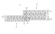
【解決手段】フレキシブルプリント配線板1は、基材4の片面に形成された第1の導体配線6を有する第1のフレキシブルプリント配線板2と、基材11の両面に形成された第2の導体配線14、15を有する第2のフレキシブルプリント配線板3を備えている。また、第1、第2のフレキシブルプリント配線板2、3の各々には、接着剤層5である異方導電性接着剤が接続される第1、第2の接続部8、18が設けられている。そして、第1の接続部8は、第1の導体配線6と略同一の高さに設けられ、第2の接続部18は、第2の導体配線14と略同一の高さに設けられている。
【選択図】 図2
Description
Claims (7)
- 第1の導体配線を有する第1のフレキシブルプリント配線板と、接着剤層を介して、前記第1の導体配線に接続される第2の導体配線を有する第2のフレキシブルプリント配線板と、を備えるフレキシブルプリント配線板において、
前記接着剤層が、導電性微粒子を含む異方導電性接着剤であるとともに、前記第1のフレキシブルプリント配線板には、前記異方導電性接着剤が接続される第1の接続部が、前記第1の導体配線と略同一の高さに設けられ、前記第2のフレキシブルプリント配線板には、前記異方導電性接着剤が接続される第2の接続部が、前記第2の導体配線と略同一の高さに設けられていることを特徴とするフレキシブルプリント配線板。 - 前記第1のフレキシブルプリント配線板が、基材の片面に形成された前記第1の導体配線を有する片面フレキシブルプリント配線板であるとともに、前記第2のフレキシブルプリント配線板が、基材の両面に形成された前記第2の導体配線を有する両面フレキシブルプリント配線板であることを特徴とする請求項1に記載のフレキシブルプリント配線板。
- 前記導電性微粒子の径が1μm以下であり、かつアスペクト比が5以上であることを特徴とする請求項1または請求項2に記載のフレキシブルプリント配線板。
- 前記導電性微粒子が、前記第1、第2の導体配線の接続前の状態において、前記接着剤層の厚み方向に配向していることを特徴とする請求項3に記載のフレキシブルプリント配線板。
- 前記第1及び第2の導体配線の少なくとも一方が、導電性ペーストにより形成されていることを特徴とする請求項4に記載のフレキシブルプリント配線板。
- 前記第1、第2のフレキシブルプリント配線板の各々に、前記異方導電性接着剤との接続を補強するための補強部材が設けられていることを特徴とする請求項1乃至請求項5のいずれかに記載のフレキシブルプリント配線板。
- 第1のフレキシブルプリント配線板において、前記第1のフレキシブルプリント配線板が有する第1の導体配線と略同一の高さに設けられた第1の接続部に、熱硬化性樹脂を主成分とする異方導電性接着剤を載置し、前記第1の接続部に前記異方導電性接着剤を接続する工程と、
前記第1の導体配線と、前記第1のフレキシブルプリント配線板に接着される第2のフレキシブルプリント配線板が有する第2の導体配線とが接続されるように、前記第1、第2のフレキシブルプリント配線板の間に前記異方導電性接着剤を介在させた状態で、前記第1のフレキシブルプリント配線板と前記第2のフレキシブルプリント配線板の位置合わせを行う工程と、
前記第2のフレキシブルプリント配線板において、前記第2の導体配線と略同一の高さに設けられた第2の接続部に、前記異方導電性接着剤を載置する工程と、
加熱加圧処理を行うことにより、前記熱硬化性樹脂を硬化させ、前記第1の導体配線と前記第2の導体配線とを接続する工程と、を少なくとも含むことを特徴とするフレキシブルプリント配線板の製造方法。
Priority Applications (6)
| Application Number | Priority Date | Filing Date | Title |
|---|---|---|---|
| JP2005272490A JP4955970B2 (ja) | 2005-09-20 | 2005-09-20 | フレキシブルプリント配線板およびその製造方法 |
| TW095134774A TWI388258B (zh) | 2005-09-20 | 2006-09-20 | 撓性印刷電路板及其製造方法 |
| CN2006800012430A CN101061760B (zh) | 2005-09-20 | 2006-09-20 | 柔性印刷电路板及其制造方法 |
| EP06798130A EP1928218B1 (en) | 2005-09-20 | 2006-09-20 | Flexible printed wiring board and method for manufacturing same |
| PCT/JP2006/318570 WO2007034801A1 (ja) | 2005-09-20 | 2006-09-20 | フレキシブルプリント配線板およびその製造方法 |
| KR1020077010588A KR20080046133A (ko) | 2005-09-20 | 2006-09-20 | 플렉서블 프린트배선판 및 그 제조방법 |
Applications Claiming Priority (1)
| Application Number | Priority Date | Filing Date | Title |
|---|---|---|---|
| JP2005272490A JP4955970B2 (ja) | 2005-09-20 | 2005-09-20 | フレキシブルプリント配線板およびその製造方法 |
Publications (2)
| Publication Number | Publication Date |
|---|---|
| JP2007088055A true JP2007088055A (ja) | 2007-04-05 |
| JP4955970B2 JP4955970B2 (ja) | 2012-06-20 |
Family
ID=37888844
Family Applications (1)
| Application Number | Title | Priority Date | Filing Date |
|---|---|---|---|
| JP2005272490A Expired - Fee Related JP4955970B2 (ja) | 2005-09-20 | 2005-09-20 | フレキシブルプリント配線板およびその製造方法 |
Country Status (6)
| Country | Link |
|---|---|
| EP (1) | EP1928218B1 (ja) |
| JP (1) | JP4955970B2 (ja) |
| KR (1) | KR20080046133A (ja) |
| CN (1) | CN101061760B (ja) |
| TW (1) | TWI388258B (ja) |
| WO (1) | WO2007034801A1 (ja) |
Cited By (8)
| Publication number | Priority date | Publication date | Assignee | Title |
|---|---|---|---|---|
| JP2007173477A (ja) * | 2005-12-21 | 2007-07-05 | Sumitomo Electric Ind Ltd | フレキシブルプリント配線板 |
| JP2009038002A (ja) * | 2007-08-03 | 2009-02-19 | Kanhin Kagaku Kofun Yugenkoshi | 異方性導電材料 |
| JP2010027762A (ja) * | 2008-07-17 | 2010-02-04 | Ricoh Co Ltd | フレキシブルプリント基板とフレキシブルフラットケーブルの接続部構造とそれを使用した液滴吐出ヘッド及び画像記録装置 |
| JP2012033597A (ja) * | 2010-07-29 | 2012-02-16 | Tokai Rubber Ind Ltd | 配線体接続構造体 |
| JP2014003001A (ja) * | 2012-06-14 | 2014-01-09 | Sumitomo Electric Ind Ltd | フラットケーブル及びその製造方法 |
| US20170374746A1 (en) * | 2015-02-13 | 2017-12-28 | Pi-Crystal Incorporation | Method for forming laminated circuit board, and laminated circuit board formed using same |
| JPWO2024070592A1 (ja) * | 2022-09-28 | 2024-04-04 | ||
| JPWO2024070591A1 (ja) * | 2022-09-28 | 2024-04-04 |
Families Citing this family (9)
| Publication number | Priority date | Publication date | Assignee | Title |
|---|---|---|---|---|
| CN102404946A (zh) * | 2010-09-13 | 2012-04-04 | 华通电脑股份有限公司 | 整合高密度多层板的低密度多层电路板及其制造方法 |
| US9884179B2 (en) | 2012-12-05 | 2018-02-06 | Bbattelle Memorial Institute | Neural sleeve for neuromuscular stimulation, sensing and recording |
| EP4201469B1 (en) * | 2012-12-05 | 2026-01-21 | Battelle Memorial Institute | Neuromuscular stimulation cuff |
| TWI549576B (zh) * | 2013-06-14 | 2016-09-11 | 財團法人工業技術研究院 | 軟性電子元件模組及其拼接結構 |
| JP6901244B2 (ja) * | 2016-07-13 | 2021-07-14 | 日本メクトロン株式会社 | フレキシブルプリント配線板の製造方法 |
| US9872390B1 (en) * | 2016-08-17 | 2018-01-16 | Microsoft Technology Licensing, Llc | Flexible interconnect |
| KR102043159B1 (ko) * | 2019-05-27 | 2019-11-11 | 주식회사 무진에이앤엘 | 증기발생기의 2차측 튜브시트 육안검사용 프로브 장치의 신호 노이즈 저감 장치 |
| TWI823350B (zh) * | 2022-04-19 | 2023-11-21 | 大陸商深圳市柯達科電子科技有限公司 | 軟性電路板連接頭、觸控式螢幕及顯示裝置 |
| DE102022124320A1 (de) | 2022-09-22 | 2024-03-28 | Audi Aktiengesellschaft | Leiterplattenanordnung, Batterieanordnung und Verfahren zum Herstellen einer Leiterplattenanordnung |
Citations (4)
| Publication number | Priority date | Publication date | Assignee | Title |
|---|---|---|---|---|
| JPH06268348A (ja) * | 1993-03-12 | 1994-09-22 | Sony Chem Corp | 複合可撓性プリント基板 |
| JPH06283226A (ja) * | 1993-07-16 | 1994-10-07 | Hitachi Chem Co Ltd | 回路の接続構造体 |
| JP2001156418A (ja) * | 1999-09-14 | 2001-06-08 | Seiko Epson Corp | 複合フレキシブル配線基板およびその製造方法、電気光学装置、電子機器 |
| JP2005146043A (ja) * | 2003-11-12 | 2005-06-09 | Sumitomo Electric Ind Ltd | 異方導電性接着剤 |
Family Cites Families (1)
| Publication number | Priority date | Publication date | Assignee | Title |
|---|---|---|---|---|
| US4731282A (en) * | 1983-10-14 | 1988-03-15 | Hitachi Chemical Co., Ltd. | Anisotropic-electroconductive adhesive film |
-
2005
- 2005-09-20 JP JP2005272490A patent/JP4955970B2/ja not_active Expired - Fee Related
-
2006
- 2006-09-20 CN CN2006800012430A patent/CN101061760B/zh not_active Expired - Fee Related
- 2006-09-20 EP EP06798130A patent/EP1928218B1/en not_active Ceased
- 2006-09-20 WO PCT/JP2006/318570 patent/WO2007034801A1/ja not_active Ceased
- 2006-09-20 KR KR1020077010588A patent/KR20080046133A/ko not_active Ceased
- 2006-09-20 TW TW095134774A patent/TWI388258B/zh not_active IP Right Cessation
Patent Citations (4)
| Publication number | Priority date | Publication date | Assignee | Title |
|---|---|---|---|---|
| JPH06268348A (ja) * | 1993-03-12 | 1994-09-22 | Sony Chem Corp | 複合可撓性プリント基板 |
| JPH06283226A (ja) * | 1993-07-16 | 1994-10-07 | Hitachi Chem Co Ltd | 回路の接続構造体 |
| JP2001156418A (ja) * | 1999-09-14 | 2001-06-08 | Seiko Epson Corp | 複合フレキシブル配線基板およびその製造方法、電気光学装置、電子機器 |
| JP2005146043A (ja) * | 2003-11-12 | 2005-06-09 | Sumitomo Electric Ind Ltd | 異方導電性接着剤 |
Cited By (13)
| Publication number | Priority date | Publication date | Assignee | Title |
|---|---|---|---|---|
| JP2007173477A (ja) * | 2005-12-21 | 2007-07-05 | Sumitomo Electric Ind Ltd | フレキシブルプリント配線板 |
| JP2009038002A (ja) * | 2007-08-03 | 2009-02-19 | Kanhin Kagaku Kofun Yugenkoshi | 異方性導電材料 |
| JP2010027762A (ja) * | 2008-07-17 | 2010-02-04 | Ricoh Co Ltd | フレキシブルプリント基板とフレキシブルフラットケーブルの接続部構造とそれを使用した液滴吐出ヘッド及び画像記録装置 |
| JP2012033597A (ja) * | 2010-07-29 | 2012-02-16 | Tokai Rubber Ind Ltd | 配線体接続構造体 |
| JP2014003001A (ja) * | 2012-06-14 | 2014-01-09 | Sumitomo Electric Ind Ltd | フラットケーブル及びその製造方法 |
| US11122693B2 (en) * | 2015-02-13 | 2021-09-14 | Pi-Crystal Incorporation | Method for forming laminated circuit board |
| US20170374746A1 (en) * | 2015-02-13 | 2017-12-28 | Pi-Crystal Incorporation | Method for forming laminated circuit board, and laminated circuit board formed using same |
| US11985768B2 (en) | 2015-02-13 | 2024-05-14 | Pi-Crystal Incorporation | Laminated circuit board |
| JPWO2024070592A1 (ja) * | 2022-09-28 | 2024-04-04 | ||
| JPWO2024070591A1 (ja) * | 2022-09-28 | 2024-04-04 | ||
| WO2024070591A1 (ja) * | 2022-09-28 | 2024-04-04 | 株式会社村田製作所 | 伸縮性デバイス |
| WO2024070592A1 (ja) * | 2022-09-28 | 2024-04-04 | 株式会社村田製作所 | 伸縮性デバイス |
| JP7718604B2 (ja) | 2022-09-28 | 2025-08-05 | 株式会社村田製作所 | 伸縮性デバイス |
Also Published As
| Publication number | Publication date |
|---|---|
| JP4955970B2 (ja) | 2012-06-20 |
| CN101061760B (zh) | 2012-11-28 |
| WO2007034801A1 (ja) | 2007-03-29 |
| KR20080046133A (ko) | 2008-05-26 |
| TWI388258B (zh) | 2013-03-01 |
| CN101061760A (zh) | 2007-10-24 |
| EP1928218A4 (en) | 2009-12-02 |
| TW200742518A (en) | 2007-11-01 |
| EP1928218A1 (en) | 2008-06-04 |
| EP1928218B1 (en) | 2012-04-11 |
Similar Documents
| Publication | Publication Date | Title |
|---|---|---|
| JP4955970B2 (ja) | フレキシブルプリント配線板およびその製造方法 | |
| CN111418272B (zh) | 柔性印刷电路板和制造柔性印刷电路板的方法 | |
| KR20100051699A (ko) | 프린트 배선판용 쉴드 필름 및 프린트 배선판 | |
| US20150000959A1 (en) | Multilayer printed circuit board having anisotropy condictive film and method for manufacturing same | |
| WO2007052584A1 (ja) | 積層回路基板の製造方法、回路板およびその製造方法 | |
| US10477704B2 (en) | Multilayer board and electronic device | |
| US20070289706A1 (en) | Process for producing multilayer board | |
| JP2008235594A (ja) | 配線板接合体およびその製造方法 | |
| KR102419510B1 (ko) | 배선 기판용 보강판 | |
| JP2007173477A (ja) | フレキシブルプリント配線板 | |
| KR101518067B1 (ko) | 다층 프린트 배선판 및 그 제조 방법 | |
| JP2012169486A (ja) | 基材、配線板、基材の製造方法及び配線板の製造方法 | |
| JP2008235346A (ja) | フレキシブルプリント配線板 | |
| TWI669035B (zh) | 電路板及電路板的製作方法 | |
| JP5515210B2 (ja) | 部品内蔵配線板、部品内蔵配線板の製造方法 | |
| JP2009043833A (ja) | 中空ヒンジ部を有する配線基板の製造方法 | |
| JP5082296B2 (ja) | 配線付き接着剤及び回路接続構造 | |
| JP2012169688A (ja) | 多層プリント配線板の製造方法 | |
| JP2012160765A (ja) | フレキシブルプリント配線板およびその製造方法 | |
| US9673063B2 (en) | Terminations | |
| JP4930712B2 (ja) | 異方性導電フィルム | |
| JP4407609B2 (ja) | 電子回路装置 | |
| JP4892924B2 (ja) | 多層プリント配線基板及びその製造方法 | |
| JP5008971B2 (ja) | 配線板およびその製造方法 | |
| JP2007258421A (ja) | フレキシブルプリント配線板およびその製造方法 |
Legal Events
| Date | Code | Title | Description |
|---|---|---|---|
| RD04 | Notification of resignation of power of attorney |
Free format text: JAPANESE INTERMEDIATE CODE: A7424 Effective date: 20080710 |
|
| RD02 | Notification of acceptance of power of attorney |
Free format text: JAPANESE INTERMEDIATE CODE: A7422 Effective date: 20080724 |
|
| A621 | Written request for application examination |
Free format text: JAPANESE INTERMEDIATE CODE: A621 Effective date: 20080901 |
|
| RD04 | Notification of resignation of power of attorney |
Free format text: JAPANESE INTERMEDIATE CODE: A7424 Effective date: 20100707 |
|
| RD03 | Notification of appointment of power of attorney |
Free format text: JAPANESE INTERMEDIATE CODE: A7423 Effective date: 20101001 |
|
| A131 | Notification of reasons for refusal |
Free format text: JAPANESE INTERMEDIATE CODE: A131 Effective date: 20110531 |
|
| A521 | Written amendment |
Free format text: JAPANESE INTERMEDIATE CODE: A523 Effective date: 20110729 |
|
| A131 | Notification of reasons for refusal |
Free format text: JAPANESE INTERMEDIATE CODE: A131 Effective date: 20111025 |
|
| A521 | Written amendment |
Free format text: JAPANESE INTERMEDIATE CODE: A523 Effective date: 20111221 |
|
| TRDD | Decision of grant or rejection written | ||
| A01 | Written decision to grant a patent or to grant a registration (utility model) |
Free format text: JAPANESE INTERMEDIATE CODE: A01 Effective date: 20120313 |
|
| A01 | Written decision to grant a patent or to grant a registration (utility model) |
Free format text: JAPANESE INTERMEDIATE CODE: A01 |
|
| A61 | First payment of annual fees (during grant procedure) |
Free format text: JAPANESE INTERMEDIATE CODE: A61 Effective date: 20120316 |
|
| R150 | Certificate of patent or registration of utility model |
Free format text: JAPANESE INTERMEDIATE CODE: R150 |
|
| FPAY | Renewal fee payment (event date is renewal date of database) |
Free format text: PAYMENT UNTIL: 20150323 Year of fee payment: 3 |
|
| R250 | Receipt of annual fees |
Free format text: JAPANESE INTERMEDIATE CODE: R250 |
|
| R250 | Receipt of annual fees |
Free format text: JAPANESE INTERMEDIATE CODE: R250 |
|
| R250 | Receipt of annual fees |
Free format text: JAPANESE INTERMEDIATE CODE: R250 |
|
| LAPS | Cancellation because of no payment of annual fees |