JP2007123721A - Method for manufacturing photoelectric conversion device and photoelectric conversion device - Google Patents
Method for manufacturing photoelectric conversion device and photoelectric conversion device Download PDFInfo
- Publication number
- JP2007123721A JP2007123721A JP2005316789A JP2005316789A JP2007123721A JP 2007123721 A JP2007123721 A JP 2007123721A JP 2005316789 A JP2005316789 A JP 2005316789A JP 2005316789 A JP2005316789 A JP 2005316789A JP 2007123721 A JP2007123721 A JP 2007123721A
- Authority
- JP
- Japan
- Prior art keywords
- thin film
- photoelectric conversion
- conversion device
- compound semiconductor
- film
- Prior art date
- Legal status (The legal status is an assumption and is not a legal conclusion. Google has not performed a legal analysis and makes no representation as to the accuracy of the status listed.)
- Pending
Links
Images

Classifications
-
- H—ELECTRICITY
- H10—SEMICONDUCTOR DEVICES; ELECTRIC SOLID-STATE DEVICES NOT OTHERWISE PROVIDED FOR
- H10F—INORGANIC SEMICONDUCTOR DEVICES SENSITIVE TO INFRARED RADIATION, LIGHT, ELECTROMAGNETIC RADIATION OF SHORTER WAVELENGTH OR CORPUSCULAR RADIATION
- H10F77/00—Constructional details of devices covered by this subclass
- H10F77/10—Semiconductor bodies
- H10F77/12—Active materials
- H10F77/126—Active materials comprising only Group I-III-VI chalcopyrite materials, e.g. CuInSe2, CuGaSe2 or CuInGaSe2 [CIGS]
-
- H—ELECTRICITY
- H10—SEMICONDUCTOR DEVICES; ELECTRIC SOLID-STATE DEVICES NOT OTHERWISE PROVIDED FOR
- H10F—INORGANIC SEMICONDUCTOR DEVICES SENSITIVE TO INFRARED RADIATION, LIGHT, ELECTROMAGNETIC RADIATION OF SHORTER WAVELENGTH OR CORPUSCULAR RADIATION
- H10F10/00—Individual photovoltaic cells, e.g. solar cells
- H10F10/10—Individual photovoltaic cells, e.g. solar cells having potential barriers
- H10F10/16—Photovoltaic cells having only PN heterojunction potential barriers
- H10F10/167—Photovoltaic cells having only PN heterojunction potential barriers comprising Group I-III-VI materials, e.g. CdS/CuInSe2 [CIS] heterojunction photovoltaic cells
-
- H—ELECTRICITY
- H10—SEMICONDUCTOR DEVICES; ELECTRIC SOLID-STATE DEVICES NOT OTHERWISE PROVIDED FOR
- H10F—INORGANIC SEMICONDUCTOR DEVICES SENSITIVE TO INFRARED RADIATION, LIGHT, ELECTROMAGNETIC RADIATION OF SHORTER WAVELENGTH OR CORPUSCULAR RADIATION
- H10F39/00—Integrated devices, or assemblies of multiple devices, comprising at least one element covered by group H10F30/00, e.g. radiation detectors comprising photodiode arrays
- H10F39/80—Constructional details of image sensors
- H10F39/803—Pixels having integrated switching, control, storage or amplification elements
-
- H—ELECTRICITY
- H10—SEMICONDUCTOR DEVICES; ELECTRIC SOLID-STATE DEVICES NOT OTHERWISE PROVIDED FOR
- H10F—INORGANIC SEMICONDUCTOR DEVICES SENSITIVE TO INFRARED RADIATION, LIGHT, ELECTROMAGNETIC RADIATION OF SHORTER WAVELENGTH OR CORPUSCULAR RADIATION
- H10F71/00—Manufacture or treatment of devices covered by this subclass
-
- H—ELECTRICITY
- H10—SEMICONDUCTOR DEVICES; ELECTRIC SOLID-STATE DEVICES NOT OTHERWISE PROVIDED FOR
- H10F—INORGANIC SEMICONDUCTOR DEVICES SENSITIVE TO INFRARED RADIATION, LIGHT, ELECTROMAGNETIC RADIATION OF SHORTER WAVELENGTH OR CORPUSCULAR RADIATION
- H10F39/00—Integrated devices, or assemblies of multiple devices, comprising at least one element covered by group H10F30/00, e.g. radiation detectors comprising photodiode arrays
- H10F39/011—Manufacture or treatment of image sensors covered by group H10F39/12
- H10F39/016—Manufacture or treatment of image sensors covered by group H10F39/12 of thin-film-based image sensors
-
- Y—GENERAL TAGGING OF NEW TECHNOLOGICAL DEVELOPMENTS; GENERAL TAGGING OF CROSS-SECTIONAL TECHNOLOGIES SPANNING OVER SEVERAL SECTIONS OF THE IPC; TECHNICAL SUBJECTS COVERED BY FORMER USPC CROSS-REFERENCE ART COLLECTIONS [XRACs] AND DIGESTS
- Y02—TECHNOLOGIES OR APPLICATIONS FOR MITIGATION OR ADAPTATION AGAINST CLIMATE CHANGE
- Y02E—REDUCTION OF GREENHOUSE GAS [GHG] EMISSIONS, RELATED TO ENERGY GENERATION, TRANSMISSION OR DISTRIBUTION
- Y02E10/00—Energy generation through renewable energy sources
- Y02E10/50—Photovoltaic [PV] energy
- Y02E10/541—CuInSe2 material PV cells
-
- Y—GENERAL TAGGING OF NEW TECHNOLOGICAL DEVELOPMENTS; GENERAL TAGGING OF CROSS-SECTIONAL TECHNOLOGIES SPANNING OVER SEVERAL SECTIONS OF THE IPC; TECHNICAL SUBJECTS COVERED BY FORMER USPC CROSS-REFERENCE ART COLLECTIONS [XRACs] AND DIGESTS
- Y02—TECHNOLOGIES OR APPLICATIONS FOR MITIGATION OR ADAPTATION AGAINST CLIMATE CHANGE
- Y02P—CLIMATE CHANGE MITIGATION TECHNOLOGIES IN THE PRODUCTION OR PROCESSING OF GOODS
- Y02P70/00—Climate change mitigation technologies in the production process for final industrial or consumer products
- Y02P70/50—Manufacturing or production processes characterised by the final manufactured product
Landscapes
- Light Receiving Elements (AREA)
- Photovoltaic Devices (AREA)
Abstract
【課題】化合物半導体薄膜(CIGS薄膜)を用いた光電変換素子(フォトセンサや太陽電池)の暗電流を劇的に低減し得る、新規な製造プロセス技術を提供する。
【解決手段】フォトリソグラフィによるエッチングによって、下部電極層(Mo)10、光吸収層として機能するカルコパイライト構造のp型の化合物半導体薄膜(CIGS薄膜)30、n型の透光性電極層(ZnO)60の各々をパターニングする手法を採用し、かつ、CIGS薄膜30については、ドライエッチングとウエットエッチングを組み合わせた2段エッチングを行うことによって、化合物半導体の結晶にダメージや欠陥を生じさせることなく、また、残渣を残すことなく、高精度のパターニングを実現する。
【選択図】図2A novel manufacturing process technology capable of dramatically reducing the dark current of a photoelectric conversion element (photosensor or solar cell) using a compound semiconductor thin film (CIGS thin film) is provided.
By etching by photolithography, a lower electrode layer (Mo) 10, a p-type compound semiconductor thin film (CIGS thin film) 30 having a chalcopyrite structure functioning as a light absorption layer, an n-type translucent electrode layer (ZnO) ) The method of patterning each of 60 is employed, and the CIGS thin film 30 is subjected to two-stage etching that combines dry etching and wet etching without causing damage or defects to the crystal of the compound semiconductor. In addition, high-precision patterning is realized without leaving a residue.
[Selection] Figure 2
Description
本発明は、光電変換装置の製造方法および光電変換装置に係り、特にカルコパイライト構造の化合物半導体薄膜を用いたフォトセンサや太陽電池等の光電変換装置に関する。 The present invention relates to a method for manufacturing a photoelectric conversion device and a photoelectric conversion device, and more particularly to a photoelectric conversion device such as a photosensor or a solar cell using a compound semiconductor thin film having a chalcopyrite structure.
Ib族元素とIIIb族元素とVIb族元素とからなる、カルコパイライト構造の半導体薄膜であるCuInSe2(CIS系薄膜)、あるいは、これにGaを固溶したCu(In,Ga)Se2(CIGS系薄膜)を光吸収層に用いた薄膜太陽電池は、高いエネルギー変換効率を示し、光照射等による効率の劣化が少ないという利点を有している。 CuInSe 2 (CIS-based thin film), which is a semiconductor thin film having a chalcopyrite structure, composed of a group Ib element, a group IIIb element, and a group VIb element, or Cu (In, Ga) Se 2 (CIGS) in which Ga is dissolved therein. A thin-film solar cell using a light-emitting layer as a light absorption layer has an advantage of exhibiting high energy conversion efficiency and little deterioration in efficiency due to light irradiation or the like.
図8(a)乃至(d)は、従来の、CIGS系薄膜太陽電池のセルの製造方法を説明するためのデバイスの断面図である。 8A to 8D are cross-sectional views of a device for explaining a conventional method for manufacturing a cell of a CIGS thin film solar battery.
図8(a)に示すように、まず、SLG(ソーダライムガラス)基板100上にプラス側の下部電極となるMo(モリブデン)電極層200が形成される。
As shown in FIG. 8A, first, a Mo (molybdenum)
次に、図8(b)に示すように、Mo電極層200上に、組成制御により、p−型を示す、CIGS系薄膜からなる光吸収層3が形成される。
Next, as shown in FIG. 8B, the
次に、図8(c)に示すように、その光吸収層3上に、CdSなどのバッファ層400を形成し、そのバッファ層400上に、不純物がドーピングされてn+型を示す、マイナス側の上部電極となるZnO(酸化亜鉛)からなる透光性電極層500を形成する。
Next, as shown in FIG. 8C, a
次に、図8(d)に示すように、メカニカルスクライブ装置によって、ZnOからなる透光性電極層500からMo電極層200までを、一括してスクライブ加工する。これによって、薄膜太陽電池の各セルが電気的に分離(すなわち、各セルが個別化)される。
Next, as shown in FIG. 8D, the mechanical scribing apparatus collectively scribes the light-transmitting
このスクライビング工程は、レーザスクライビング(レーザ光を照射することによって薄膜を部分的に除去するスクライブ技術)を利用することもできる。 This scribing process can also use laser scribing (a scribing technique for partially removing a thin film by irradiating laser light).
しかし、この場合には、レーザ光を集中的に照射するために、局部的に高熱が発生し、これによってセルの特性が劣化するという不都合が生じる。 However, in this case, since laser light is intensively irradiated, high heat is locally generated, which causes a disadvantage that the characteristics of the cell deteriorate.
したがって、太陽電池のセルは、一般に、メカニカルスクライビング装置によって電気的に分離される。 Therefore, the cells of the solar battery are generally electrically separated by a mechanical scribing device.
特許文献1に記載のメカニカルスクライブ装置では、所定のテーパー角度をもって先細りになり、かつ先端が平坦な刃を、所定の圧力をもって被加工面のスクライブ箇所に垂直に押し付け、その刃を被加工面に沿って移動させることによってスクライブ加工を行っている。
CIS系薄膜、CIGS系薄膜は、太陽電池としての利用が主流である。 CIS thin films and CIGS thin films are mainly used as solar cells.
一方、本発明者らは、この化合物半導体薄膜材料の高い光吸収係数と、可視光から近赤外光までの広い波長域に渡って高い感度をもつ特性に着目し、この化合物半導体薄膜材料を、セキュリティカメラ(昼間は可視光をセンシングし、夜間は近赤外光をセンシングするカメラ)や、個人認証カメラ(外光の影響を受けない近赤外光で個人認証するためのカメラ)、あるいは、車載カメラ(夜間の視覚補助や遠方の視野確保等にために車に搭載されるカメラ)用のイメージセンサとして利用することについて検討した。 On the other hand, the present inventors paid attention to the high light absorption coefficient of this compound semiconductor thin film material and the property of having high sensitivity over a wide wavelength range from visible light to near infrared light. Security cameras (cameras that sense visible light during the day and near-infrared light at night), personal authentication cameras (cameras that authenticate with near-infrared light that is not affected by external light), or We examined the use as an image sensor for in-vehicle cameras (cameras mounted on cars for night vision assistance and distant vision).
この結果として、CIS系薄膜(CuInSe2)を例にとると、暗電流(逆バイアス時にPN接合に流れる電流)が予想外に大きいことがわかった。 As a result, it was found that when a CIS thin film (CuInSe 2 ) was taken as an example, the dark current (current flowing through the PN junction during reverse bias) was unexpectedly large.
すなわち、例えば、−0.8Vの逆バイアス時に、1×10⁻³A/cm2程度の暗電流が流れ、この値は、シリコン系材料よりも6桁大きい。このままでは、1000Lux(ルクス)以下の弱い光は、雑音に埋もれてしまい、検出できないことになる。 That is, for example, a dark current of about 1 × 10 −3 A / cm 2 flows at a reverse bias of −0.8 V, and this value is six orders of magnitude larger than that of a silicon-based material. In this state, weak light of 1000 Lux or less is buried in noise and cannot be detected.
そこで、暗電流を大幅に低減する必要が生じた。本発明の発明者は、化合物半導体薄膜において暗電流が増大する要因を詳細に調べたが、その結果、メカニカルスクライビング時に化合物半導体材料の結晶にダメージや欠陥が生じ、これにより、PN接合の界面に複数のエネルギー準位が発生し、これが大きな暗電流の要因となることがわかった。 Therefore, it has become necessary to significantly reduce the dark current. The inventor of the present invention investigated in detail the factors that increase the dark current in the compound semiconductor thin film. As a result, the crystal of the compound semiconductor material is damaged or defective during mechanical scribing, and this causes the interface of the PN junction. It was found that a plurality of energy levels were generated, which caused a large dark current.
すなわち、図8(d)において、PN接合の界面(空乏層の境界:点線で示す)の端部(図中、丸で囲んで示すA,B部分)は、メカニカルスクライビングされて露出するCIGS薄膜300の側壁に到達している。メカニカルスクライビング面は、結晶のダメージが大きく、不要な界面順位が存在する。したがって、この部分で、PN接合のリーク電流が増大してしまう。 That is, in FIG. 8D, the CIGS thin film is exposed by mechanical scribing at the end portions (A and B portions surrounded by circles in the figure) of the interface of the PN junction (boundary of depletion layer: indicated by dotted line). 300 side walls have been reached. The mechanical scribing surface has a large crystal damage and has an unnecessary interface order. Therefore, the leakage current of the PN junction increases at this portion.
本発明は、このような考察に基づいてなされたものであり、化合物半導体薄膜を用いた光電変換素子の暗電流を大幅に低減することを目的とする。 This invention is made | formed based on such consideration, and it aims at reducing the dark current of the photoelectric conversion element using a compound semiconductor thin film significantly.
本発明の光電変換装置の製造方法は、基板上に下部電極層、光吸収層として機能するカルコパイライト構造の化合物半導体薄膜、透光性電極層が積層されて構成される光電変換装置の製造方法であって、前記カルコパイライト構造の化合物半導体薄膜をフォトリソグラフィによってパターニングする工程を含む。 The method for producing a photoelectric conversion device according to the present invention is a method for producing a photoelectric conversion device comprising a lower electrode layer, a compound semiconductor thin film having a chalcopyrite structure that functions as a light absorption layer, and a light-transmitting electrode layer. The method includes a step of patterning the compound semiconductor thin film having the chalcopyrite structure by photolithography.
この構成によれば、メカニカルスクライビングの代わりに、フォトリソグラフィによるエッチングによって、カルコパイライト構造の化合物半導体薄膜をパターニングするものである。これに伴い、下部電極層、透光性電極層の各々もフォトリソグラフィを用いたエッチングによってパターニングされることになる。これによって、メカニカルスクライビングを行ったときのような、ダメージや欠陥が化合物半導体薄膜に生じず、暗電流の大幅な低減が可能となる。 According to this configuration, the compound semiconductor thin film having a chalcopyrite structure is patterned by photolithography etching instead of mechanical scribing. Along with this, each of the lower electrode layer and the translucent electrode layer is also patterned by etching using photolithography. As a result, no damage or defect occurs in the compound semiconductor thin film as in mechanical scribing, and the dark current can be greatly reduced.
また、本発明の光電変換装置の製造方法は、前記カルコパイライト構造の化合物半導体薄膜をパターニングする工程は、ドライエッチングによりパターニングする第1の工程と、この第1の工程で生じるエッチング残渣を、ウエットエッチングより除去する第2の工程と、を含む。 In the method for manufacturing a photoelectric conversion device according to the present invention, the step of patterning the chalcopyrite-structured compound semiconductor thin film includes a first step of patterning by dry etching and an etching residue generated in the first step. And a second step of removing by etching.
光吸収層として機能するカルコパイライト構造の化合物半導体薄膜のパターニングに際し、ドライエッチングとウエットエッチングを組み合わせた2段エッチングを行い、これによって、残渣がなく、精度の高いパターン形成を実現するものである。光吸収層として機能するカルコパイライト構造のp型の化合物半導体薄膜は、ドライエッチングを用いてエッチング可能であるが、この場合は完全なエッチングができず、多数の柱状の残渣が残る。また、ウエットエッチングでは、サイドエッチング(レジストパターンの直下の部分について横方向のエッチングが進む現象)によってアンダーカットが生じ、精度よくパターンを形成することができない。そこで、ドライエッチングによって、サイドエッチングなく化合物半導体薄膜をパターニングし、その後の短時間のウエットエッチング処理によって、ドライエッチングの残渣のみを除去するようにし、これによって、残渣を生じさせることなく、高精度のパターンを形成することが可能となる。これによって、メカニカルエッチングを採用したときのような、ダメージや欠陥が化合物半導体の結晶に生じず、暗電流の大幅な低減が可能となる。 When patterning a compound semiconductor thin film having a chalcopyrite structure functioning as a light absorbing layer, two-stage etching combining dry etching and wet etching is performed, thereby realizing a highly accurate pattern formation with no residue. A p-type compound semiconductor thin film having a chalcopyrite structure functioning as a light absorption layer can be etched using dry etching. In this case, complete etching cannot be performed, and a large number of columnar residues remain. In wet etching, undercuts occur due to side etching (a phenomenon in which lateral etching proceeds in a portion immediately below the resist pattern), and the pattern cannot be formed with high accuracy. Therefore, by patterning the compound semiconductor thin film without side etching by dry etching, and removing only the dry etching residue by a subsequent short-time wet etching process, thereby achieving high precision without causing residue. A pattern can be formed. As a result, no damage or defect occurs in the crystal of the compound semiconductor as in the case of employing mechanical etching, and the dark current can be greatly reduced.
また、本発明の光電変換装置の製造方法は、前記第1の工程では、塩素系ガスをエッチャントとしてドライエッチングを行い、また、前記第2の工程では、前記カルコパイライト構造の化合物半導体薄膜を、臭素とメタノールの混合液、または、水とアンモニアの混合液で処理した後、塩酸と硝酸の混合液で処理するようにしたものを含む。 In the method for manufacturing a photoelectric conversion device of the present invention, in the first step, dry etching is performed using a chlorine-based gas as an etchant, and in the second step, the chalcopyrite structured compound semiconductor thin film is formed. Including those treated with a mixed solution of bromine and methanol or a mixed solution of water and ammonia and then treated with a mixed solution of hydrochloric acid and nitric acid.
ドライエッチングのエッチャントとして塩素系ガスを用いることによって、光吸収層を構成する化合物半導体薄膜を高レートでエッチングできる。また、ウエットエッチングについても、効率的かつ完全に残渣を除去することができる。 By using a chlorine-based gas as an etchant for dry etching, the compound semiconductor thin film constituting the light absorption layer can be etched at a high rate. Also, with respect to wet etching, the residue can be removed efficiently and completely.
また、本発明の光電変換装置の製造方法は、前記カルコパイライト構造の化合物半導体薄膜は、Cu(Inx,Ga(1-x))Se2(0≦x≦1)であるものを含む。 In the method for manufacturing a photoelectric conversion device according to the present invention, the compound semiconductor thin film having a chalcopyrite structure includes Cu (In x , Ga (1-x) ) Se 2 (0 ≦ x ≦ 1).
暗電流の低減には、CIS系薄膜(CuInSe2)のバンドギャップの広幅化が有効であり、そこで、In(インジウム)の一部をガリウムに置換したCIGS系薄膜を使用するものである。バンド幅を広げることによって、キャリアの再結合過程を減らすことができ、暗電流を低減することができる。
なおカルコパイライト構造の化合物半導体薄膜としては、このほかCuAlS2,CuAlSe2, CuAlTe2,CuGaS2,CuGaSe2,CuGaTe2,CuInS2,CuInSe2,CuInTe2,AgAlS2,AgAlSe2,AgAlTe2,AgGaS2,AgGaSe2, AgGaTe2, AgInS2, AgInSe2, AgInTe2など、他の化合物半導体薄膜も適用可能である。
In order to reduce the dark current, it is effective to widen the band gap of the CIS thin film (CuInSe 2 ). Therefore, a CIGS thin film in which a part of In (indium) is substituted with gallium is used. By widening the bandwidth, the carrier recombination process can be reduced and the dark current can be reduced.
In addition, as the compound semiconductor thin film of chalcopyrite structure, CuAlS 2 , CuAlSe 2 , CuAlTe 2 , CuGaS 2 , CuGaSe 2 , CuGaTe 2 , CuInS 2 , CuInSe 2 , CuInTe 2 , AgAlS 2 , AgAlSe 2 , AgAlTe 2 , AgGaS Other compound semiconductor thin films such as 2, AgGaSe 2 , AgGaTe 2 , AgInS 2 , AgInSe 2 , AgInTe 2 are also applicable.
また、本発明の光電変換装置の製造方法前記カルコパイライト構造の化合物半導体薄膜を形成する工程は、PVD法により、Cu(Inx,Ga(1-x))Se2(0≦x≦1)薄膜を成膜する工程を含み、前記透光性電極層を形成する工程は、前記化合物半導体薄膜上にノンドープのZnO膜を形成する工程と、前記ノンドープのZnO膜上にn+型のZnO膜とを形成する工程を含むものを含む。 In addition, the process for forming the compound semiconductor thin film having the chalcopyrite structure according to the present invention includes Cu (In x , Ga (1-x) ) Se 2 (0 ≦ x ≦ 1) by the PVD method. The step of forming the light-transmitting electrode layer includes a step of forming a non-doped ZnO film on the compound semiconductor thin film, and an n + -type ZnO film on the non-doped ZnO film. Including the step of forming.
この構成によれば、透光性電極層としてノンドープのZnO膜(i−ZnO)を設けることにより、下地のCIGS薄膜に生じるボイドやピンホールを半絶縁層で埋め込むと共に、CIGS薄膜とi−p接合を形成し、導電性のZnO膜(n+)をCIGS薄膜と直接に接触させた場合に起こるトンネル電流によるリークを防ぐことができる。したがって、ノンドープのZnO膜(i−ZnO)を厚膜化することによって、PN接合界面の暗電流を低減することができる。ここでPVD法とは、真空中で蒸発させた原材料を堆積させて成膜する方法をいうものとする。 According to this configuration, by providing a non-doped ZnO film (i-ZnO) as the translucent electrode layer, voids and pinholes generated in the underlying CIGS thin film are embedded in the semi-insulating layer, and the CIGS thin film and the i-p It is possible to prevent leakage due to a tunnel current that occurs when a junction is formed and the conductive ZnO film (n + ) is brought into direct contact with the CIGS thin film. Therefore, the dark current at the PN junction interface can be reduced by increasing the thickness of the non-doped ZnO film (i-ZnO). Here, the PVD method refers to a method of forming a film by depositing raw materials evaporated in a vacuum.
また、本発明の光電変換装置は、本発明の光電変換装置の製造方法によって製造された光電変換装置である。 Moreover, the photoelectric conversion device of the present invention is a photoelectric conversion device manufactured by the method for manufacturing a photoelectric conversion device of the present invention.
本発明の光電変換装置は、フォトリソグラフィを用いて、残渣を残さずに精度良くパターニングされており、メカニカルスクライビングを採用したときのような、ダメージや欠陥が化合物半導体の結晶に生じず、したがって、PN接合の界面に無用なエネルギー準位が生じず、暗電流の劇的な低減が可能である。すなわち、製造プロセスを変更し、光吸収層や透光性電極層のデバイス構造を最適化することによって、暗電流を103のオーダで、改善することができる。また、Cu(Inx,Ga(1-x))Se2でのバンドギャップコントロールによって、暗電流を102のオーダで、低減することができる。 The photoelectric conversion device of the present invention is accurately patterned without leaving a residue using photolithography, and damage and defects do not occur in the compound semiconductor crystal as when mechanical scribing is employed. Unnecessary energy levels are not generated at the interface of the PN junction, and the dark current can be dramatically reduced. That is, the dark current can be improved on the order of 103 by changing the manufacturing process and optimizing the device structure of the light absorption layer and the light transmitting electrode layer. Further, the dark current can be reduced on the order of 102 by the band gap control in Cu (In x , Ga (1-x) ) Se 2 .
また、本発明の光電変換装置の一態様では、近赤外光領域にも感度をもつフォトセンサである。 One embodiment of the photoelectric conversion device of the present invention is a photosensor having sensitivity also in the near-infrared light region.
暗電流が大幅に低減された、化合物半導体薄膜を使用してフォトセンサ(イメージセンサ)を形成することによって得られた、本発明のセンサは、近赤外光にも高い感度を有するため、セキュリティカメラ(昼間は可視光をセンシングし、夜間は近赤外光をセンシングするカメラ)や、個人認証カメラ(外光の影響を受けない近赤外光で個人認証するためのカメラ)、あるいは、車載カメラ(夜間の視覚補助や遠方の視野確保等にために車に搭載されるカメラ)として、十分に利用可能である。 Since the sensor of the present invention obtained by forming a photosensor (image sensor) using a compound semiconductor thin film, in which the dark current is greatly reduced, has high sensitivity to near infrared light, security. Camera (camera that senses visible light in the daytime and near-infrared light at night), personal authentication camera (camera for personal authentication with near-infrared light that is not affected by external light), or in-vehicle It can be used as a camera (camera mounted on a car for night vision assistance or securing a far field of view).
また、本発明の光電変換装置は、太陽電池である。 The photoelectric conversion device of the present invention is a solar cell.
本発明の光電変換は、PN接合の界面における光電変換ロスが、従来に比べて、十分に低減されているため、光により発生した電荷の収集効率が高く、光電変換効率が高い太陽電池を実現することができる。 In the photoelectric conversion of the present invention, the photoelectric conversion loss at the interface of the PN junction is sufficiently reduced compared to the conventional one, so that the collection efficiency of charges generated by light is high, and a solar cell with high photoelectric conversion efficiency is realized. can do.
本発明によれば、フォトリソグラフィによるエッチングによって、下部電極層、光吸収層として機能するカルコパイライト構造の化合物半導体薄膜をパターニングする手法を採用することによって、メカニカルスクライビングを行ったときのような、ダメージや欠陥が化合物半導体薄膜に生じず、暗電流の大幅な低減が可能となる。 According to the present invention, by employing a technique of patterning a compound semiconductor thin film having a chalcopyrite structure that functions as a lower electrode layer and a light absorption layer by etching by photolithography, damage such as when mechanical scribing is performed. As a result, no dark current is generated in the compound semiconductor thin film, and the dark current can be greatly reduced.
また、光吸収層については、ドライエッチングとウエットエッチングを組み合わせた2段エッチングを行うことによって、化合物半導体薄膜の結晶にダメージや欠陥を生じさせることなく、また、残渣を残さずに、高精度なパターニングを実現することができる。 In addition, the light absorbing layer is subjected to two-stage etching that combines dry etching and wet etching, so that the crystal of the compound semiconductor thin film is not damaged or defective, and no residue is left. Patterning can be realized.
また、ドライエッチングのエッチャントとして塩素系ガスを用いることによって、光吸収層を構成する化合物半導体薄膜を高レートで精度よくエッチングできる。また、ウエットエッチングについても、効率的かつ完全に残渣を除去することができる。 Further, by using a chlorine-based gas as an etchant for dry etching, the compound semiconductor thin film constituting the light absorption layer can be etched at a high rate and with high accuracy. Also, with respect to wet etching, the residue can be removed efficiently and completely.
また、光吸収層となる化合物半導体薄膜として、In(インジウム)の一部をガリウムに置換したCIGS系薄膜を使用し、バンド幅を広げることによって、キャリアの再結合過程を減らすことができ、暗電流を低減することができる(1/5に低減)。 In addition, the CIGS thin film in which a part of In (indium) is replaced with gallium is used as the compound semiconductor thin film that becomes the light absorption layer, and the carrier recombination process can be reduced by widening the bandwidth. The current can be reduced (reduced to 1/5).
また、本発明の光電変換装置は、フォトリソグラフィを用いて、残渣を残さずに精度良くスクライビングされており、メカニカルスクライビングを採用したときのような、ダメージや欠陥が化合物半導体の結晶に生じず、したがって、PN接合の界面に無用なエネルギー準位が生じず、暗電流の大幅な低減が可能である。すなわち、製造プロセスを変更して、光吸収層ならびに透光性電極層のデバイス構造を最適化することによって、暗電流を103のオーダで、改善することができる。また、Cu(Inx,Ga(1-x))Se2でのバンドギャップコントロールによって、暗電流を102のオーダで、低減することができる。 In addition, the photoelectric conversion device of the present invention is scribed with high accuracy without leaving a residue using photolithography, and damage and defects do not occur in the compound semiconductor crystal, as when mechanical scribing is employed, Therefore, useless energy levels are not generated at the interface of the PN junction, and the dark current can be greatly reduced. That is, the dark current can be improved on the order of 103 by changing the manufacturing process and optimizing the device structure of the light absorbing layer and the light transmitting electrode layer. Further, the dark current can be reduced on the order of 102 by the band gap control in Cu (In x , Ga (1-x) ) Se 2 .
本発明のセンサは、近赤外光にも高い感度を有するため、セキュリティカメラ(昼間は可視光をセンシングし、夜間は近赤外光をセンシングするカメラ)や、個人認証カメラ(外光の影響を受けない近赤外光で個人認証するためのカメラ)、あるいは、車載カメラ(夜間の視覚補助や遠方の視野確保等にために車に搭載されるカメラ)として、十分に利用可能である。 Since the sensor of the present invention has high sensitivity to near-infrared light, a security camera (a camera that senses visible light during the day and a near-infrared light at night) and a personal authentication camera (the influence of external light). It can be sufficiently used as a camera for personal authentication using near-infrared light that does not receive light, or a vehicle-mounted camera (a camera mounted in a car for night vision assistance or securing a far vision).
また、本発明の光電変換は、PN接合の界面における光電変換ロスが、従来に比べて、十分に低減されているため、光により発生した電荷の収集効率が高く、光電変換効率が高い太陽電池を実現することができる。 Further, the photoelectric conversion of the present invention has a sufficiently low photoelectric conversion loss at the interface of the PN junction as compared with the conventional case, so that the collection efficiency of charges generated by light is high and the solar cell has high photoelectric conversion efficiency. Can be realized.
次に、本発明の実施の形態について、図面を参照して説明する。
(実施の形態1)
Next, embodiments of the present invention will be described with reference to the drawings.
(Embodiment 1)
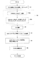
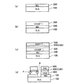
図1は、本発明にかかる光電変換装置の製造方法の概要を示すフロー図である。 FIG. 1 is a flowchart showing an outline of a method for manufacturing a photoelectric conversion device according to the present invention.
本製造プロセスでは、積層形成される下部電極層、光吸収層として機能するカルコパイライト構造のp型の化合物半導体薄膜(以下、CIGS薄膜という)、透光性電極層(ノンドープの部分と、不純物がドープされてn+型を示す部分の双方を含んでいる)の各々を、フォトリソフラフィ技術を用いてパターニングし、CIGS薄膜の結晶に与えるダメージを最小限に抑えるようにしたことを特徴とする。 In this manufacturing process, a laminated lower electrode layer, a p-type compound semiconductor thin film (hereinafter referred to as a CIGS thin film) having a chalcopyrite structure functioning as a light absorption layer, a translucent electrode layer (non-doped portion, impurities) Each of which is doped to include an n + -type portion) and is patterned using photolithographic techniques to minimize damage to the CIGS thin film crystals. .
すなわち、本発明の光電変換装置の製造方法は、ガラス基板上に下部電極となるMo(モリブデン)層をスパッタ法により成膜し(0.6μm程度)、その後、フォトリソグラフィを用いてパターニングする(工程S1)。これによって、電気的に分離されたMoのアイランド領域が形成される。 That is, in the method for manufacturing a photoelectric conversion device of the present invention, a Mo (molybdenum) layer serving as a lower electrode is formed on a glass substrate by sputtering (about 0.6 μm), and then patterned using photolithography ( Step S1). As a result, an electrically isolated island region of Mo is formed.
次に、CIGS薄膜の成膜と、フォトリソグラフィを用いたパターニングを行う(工程S2)。この工程S2が、本発明の製造方法の最も重要な特徴点となる。 Next, a CIGS thin film is formed and patterning is performed using photolithography (step S2). This step S2 is the most important feature point of the production method of the present invention.
すなわち、組成制御されたp−型のCIGS薄膜(Cu(Inx,Ga(1-x))Se2(0≦x≦1))を、例えば、イオンビームスパッタ法によって成膜する(工程S2a)。その厚みは、1.7μm程度である。 That is, a compositionally controlled p - type CIGS thin film (Cu (Inx, Ga (1-x)) Se2 (0 ≦ x ≦ 1)) is formed by, for example, an ion beam sputtering method (step S2a). Its thickness is about 1.7 μm.
次に、そのCIGS薄膜(p−)を、ドライエッチングとウエットエッチングを併用した2段エッチングによってパターニングする(工程S2b)。これにより、電気的に分離されたCIGS薄膜(p−)が得られる。 Next, the CIGS thin film (p − ) is patterned by two-stage etching using both dry etching and wet etching (step S2b). Thereby, an electrically separated CIGS thin film (p − ) is obtained.
次に、バッファ層(窓層)としての、薄いCdS膜(50nm程度)を溶液成長法により成膜する(工程S3)。 Next, a thin CdS film (about 50 nm) as a buffer layer (window layer) is formed by a solution growth method (step S3).
次に、スパッタ法により、ノンドープのZnO膜(i−ZnO)と、不純物がドープされた低抵抗のZnO(n+)膜を連続的に成膜する(工程S4)。ここで、i−ZnOは60nm程度と薄く、一方、低抵抗化のZnO(n+)は、1μm程度と十分な厚みがある。 Next, a non-doped ZnO film (i-ZnO) and a low-resistance ZnO (n + ) film doped with impurities are successively formed by sputtering (step S4). Here, i-ZnO is as thin as about 60 nm, while low-resistance ZnO (n + ) has a sufficient thickness of about 1 μm.
ノンドープのZnO膜(i−ZnO)は、下地のCIGS薄膜に生じるボイドやピンホールを半絶縁層で埋め込むと共に、CIGS薄膜とi−p接合を形成し、低抵抗のZnO膜(n+)をCIGS薄膜と直接に接触させた場合に起こるトンネル電流によるリークを防ぐ役割を果たす。 The non-doped ZnO film (i-ZnO) embeds voids and pinholes generated in the underlying CIGS thin film with a semi-insulating layer and forms an ip junction with the CIGS thin film to form a low resistance ZnO film (n + ). It plays a role of preventing leakage due to tunneling current that occurs when it is brought into direct contact with the CIGS thin film.
したがって、ノンドープのZnO膜(i−ZnO)を厚膜化することによって、PN接合界面の暗電流を低減することができる(約1/5とする効果が確認された)。但し、厚膜化するといっても、その厚みは十分に薄いため(例えば、60nm)、透光性電極層として機能する低抵抗のZnO(n+)膜とCIGS薄膜(p−)との間で実質的なpn接合が形成されると考えられる。 Therefore, by increasing the thickness of the non-doped ZnO film (i-ZnO), the dark current at the PN junction interface can be reduced (an effect of approximately 1/5 was confirmed). However, even if the film thickness is increased, the thickness is sufficiently thin (for example, 60 nm), so that the low resistance ZnO (n + ) film functioning as a translucent electrode layer and the CIGS thin film (p − ) Thus, it is considered that a substantial pn junction is formed.
次に、ZnO膜(i−ZnOとZnO(n+))をパターニングする(工程S5)。この工程S5では、ZnO膜の端部の位置が、パターニングされたCIGS薄膜(p−)の側面よりも内側になるようにパターニングする(すなわち、CIGS薄膜(p−)の上に、このCIGS薄膜(p−)よりも横幅が狭いZnO膜が形成されて、親亀子亀構造が形成されることになる)。 Next, the ZnO film (i-ZnO and ZnO (n + )) is patterned (step S5). In this step S5, the position of the end portion of the ZnO film is patterned CIGS thin film (p -) is patterned such that the inside than the side surface (i.e., CIGS thin film (p - over), the CIGS thin film A ZnO film having a narrower width than (p − ) is formed, and a parent turtle structure is formed).
これにより、ZnO(n+)とCIGS薄膜(p−)とによって形成されるPN接合の界面(空乏層の境界)の端部が、パターニングされたCIGS薄膜(p−)の側壁(エッチングにより露出している面)に達することがなく、これによって、PN接合界面の埋込み構造が実現される。 As a result, the end portion of the interface (depletion layer boundary) of the PN junction formed by ZnO (n + ) and the CIGS thin film (p − ) is exposed on the side wall (etched by etching) of the patterned CIGS thin film (p − ). Thus, a buried structure of the PN junction interface is realized.
フォトリソグラフィによりパターニングされたCIGS薄膜(p−)の側面は、メカニカルスクライビングの場合に比べ、結晶欠陥やダメージは十分に少ないが、それでも、ダングリングボンド(結合手)等が存在して不要なエネルギー準位が形成されることがないとはいえない。したがって、PN接合界面の端部が、このパターニングされたCIGS薄膜(p−)の側面(エッチングにより露出している面)に達しないようにすることによって、PN接合の界面の端部からのリーク電流を、さらに低減できる。 The side surface of the CIGS thin film (p − ) patterned by photolithography has fewer crystal defects and damage than mechanical scribing, but it still has dangling bonds (bonds) and other unnecessary energy. It cannot be said that no level is formed. Therefore, by preventing the end portion of the PN junction interface from reaching the side surface (surface exposed by etching) of the patterned CIGS thin film (p − ), leakage from the end portion of the PN junction interface is prevented. The current can be further reduced.
最後に、引き出し電極を形成する(工程S6)。これによって光電変換デバイスが完成する。 Finally, lead electrodes are formed (step S6). Thereby, a photoelectric conversion device is completed.
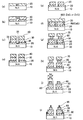
次に、図2を参照して、本発明の光電変換装置の製造方法を具体的に説明する。 Next, with reference to FIG. 2, the manufacturing method of the photoelectric conversion apparatus of this invention is demonstrated concretely.
図2(a)乃至(j)は、本発明の光電変換装置の製造方法を具体的に説明するための、主要な工程毎のデバイスの断面図である。 2A to 2J are cross-sectional views of a device for each main process for specifically explaining the method for manufacturing a photoelectric conversion device of the present invention.
なお、以下の説明では、図3(a)、(b)ならびに図4を、適宜、参照する。ここで、図3は、CIGS薄膜のパターニング方法を説明するためのデバイスのSEM(走査顕微鏡)による1万倍の拡大写真を模式化して示す図であり、(a)は、CIGS薄膜のドライエッチング直後の状態を示す図であり、(b)は、さらにウエットエッチングを行った後の状態を示す図である。 In the following description, FIGS. 3A and 3B and FIG. 4 are referred to as appropriate. Here, FIG. 3 is a diagram schematically showing a 10,000 times magnified photograph of a device by SEM (scanning microscope) for explaining a CIGS thin film patterning method, and (a) is a dry etching of a CIGS thin film. It is a figure which shows the state immediately after, (b) is a figure which shows the state after performing further wet etching.
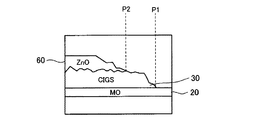
また、図4は、透光性電極層(ZnO膜)のパターニング後のデバイスのSEM(走査顕微鏡)の断面写真(2万倍の拡大写真)を模式化して示す図である。 FIG. 4 is a diagram schematically showing a cross-sectional photograph (magnified photograph of 20,000 times) of an SEM (scanning microscope) of the device after patterning of the translucent electrode layer (ZnO film).
まず、図2(a)に示すように、ソーダライムガラス基板(SLG)10上に、スパッタ法によりMo(モリブデン)膜を0.6μmの厚さで形成する。 First, as shown in FIG. 2A, a Mo (molybdenum) film having a thickness of 0.6 μm is formed on a soda lime glass substrate (SLG) 10 by sputtering.
図2(b)に示すように、例えば、Cu:In:Ga:Se=1:0.5:0.5:2の組成のスパッタターゲットを使用してイオンビームスパッタ法によってCIGS薄膜30を1.7μmの厚さで形成する。
As shown in FIG. 2B, for example, the CIGS
図2(c)に示すように、レジストパターン40を用いて、CIGS薄膜30を、ドライエッチングする。すなわち、塩素系ガスをエッチャントとして用いて、CIGS薄膜30を垂直にエッチングしてパターニングを行う。この場合、高いレートで、サイドエッチがほとんどないエッチングが可能であるが、多数の残渣35が残る(図3(a)からわかるように、多数のMo膜上に多数の柱状の残渣が残存している)。
As shown in FIG. 2C, the CIGS
そこで、図2(d)に示すように、臭素とメタノールの混合液、または、水とアンモニアの混合液で処理した後、塩酸と硝酸の混合液で処理して、残渣35を完全に除去する。図3(b)に示すように、残渣35は完全に除去される。
Therefore, as shown in FIG. 2 (d), after treatment with a mixed solution of bromine and methanol or a mixed solution of water and ammonia, treatment with a mixed solution of hydrochloric acid and nitric acid completely removes the
このように、ドライエッチングのエッチャントとして塩素系ガスを用いることによって、光吸収層を構成するCIGS薄膜30を高レートで、アンダーカットを生じさせることなく高精度にエッチングできる。その後、短時間のウエットエッチングを実施して、柱状の残渣35を完全に除去する。これによって、残渣を生じさせることなく、高精度のCIGS薄膜のパターンニングが可能となる。この場合、メカニカルエッチングを採用したときのような、ダメージや欠陥がCIGS薄膜30の結晶に生じず、暗電流の大幅な低減が可能となる。
As described above, by using a chlorine-based gas as an etchant for dry etching, the CIGS
次に、レジストパターン40を除去する。この状態のデバイス断面を図2(e)に示す。
Next, the resist
図2(f)に示すように、バッファ層(窓層)としての、薄いCdS膜50(50nm程度)をスパッタ法により成膜し、続いて、スパッタ法により、ZnO膜60を成膜する。
As shown in FIG. 2F, a thin CdS film 50 (about 50 nm) as a buffer layer (window layer) is formed by sputtering, and then a
ZnO膜60は、ノンドープのZnO膜(i−ZnO)と、n型不純物がドープされた、低抵抗のZnO(n+)膜(図中、n−ZnOと表記されている)を、連続的に成膜することによって形成される。ここで、i−ZnOの厚みは60nm程度であり、一方、低抵抗化のZnO(n+)の厚みは、1μm程度である。
The
ノンドープのZnO膜(i−ZnO)は、下地のCIGS薄膜に生じるボイドやピンホールを半絶縁層で埋め込むと共に、CIGS薄膜30とi−p接合を形成し、トンネル電流によるリークを防ぐ役割を果たす。
The non-doped ZnO film (i-ZnO) fills voids and pinholes generated in the underlying CIGS thin film with a semi-insulating layer and forms an ip junction with the CIGS
したがって、ノンドープのZnO膜(i−ZnO)を厚膜化することによって、PN接合界面の暗電流を低減することができる。但し、厚膜化するとはいえ、その厚みは十分に薄いため(例えば、60nm)、透光性電極層として機能する低抵抗のZnO(n+)膜とCIGS薄膜(p−)との間で実質的なpn接合が形成されると考えられる。 Therefore, the dark current at the PN junction interface can be reduced by increasing the thickness of the non-doped ZnO film (i-ZnO). However, although the thickness is increased, the thickness is sufficiently thin (for example, 60 nm), and therefore, between the low-resistance ZnO (n + ) film functioning as a translucent electrode layer and the CIGS thin film (p − ). It is considered that a substantial pn junction is formed.
次に、図2(g)に示すように、エッチングマスクとしてレジストパターン70を形成した後、ZnO膜(i−ZnOとZnO(n+))30をウエットエッチングする。
Next, as shown in FIG. 2G, after forming a resist
すなわち、例えば、塩酸:水=1:10の希酸を用いて、ウエットエッチングを行う。このとき、エッチング時間を調整し、意図的に、サイドエッチを生じさせ、レジストパターン70の下にアンダーカットを生じさせる。これは、パターニングされたZnO膜60の端部の位置が、パターニングされたCIGS(p−)薄膜60の側面よりも内側になるようにするためである。
That is, for example, wet etching is performed using dilute acid of hydrochloric acid: water = 1: 10. At this time, the etching time is adjusted to intentionally cause side etching, thereby causing an undercut under the resist
次に、レジストパターン70を用いてドライエッチングを行い、CIGS薄膜30の側壁上のCdS膜50を除去する。この状態のデバイスの断面構造が図2(h)に示されている。
Next, dry etching is performed using the resist
次に、図2(i)に示すよう、レジストパターン70を除去する。図示すように、ZnO膜60の横幅W2は、CIGS(p−)薄膜30の横幅W1よりも狭く、これによって、親亀子亀構造が形成されている。図4から明らかなように、ZnO膜60の端部の位置P2は、CIGS薄膜30の側壁の位置P1よりも内側に位置している。
Next, as shown in FIG. 2I, the resist
この結果、図2(i)に示すように、ZnO(n+)膜60とCIGS(p−)薄膜30によって形成されるPN接合の界面80(空乏層の境界:図中、点線で示されている)の端部が、パターニングされたCIGS(p−)薄膜30の側壁(エッチングにより露出した面)に達することがなく、これによって、PN接合界面の埋込み構造が実現される。
As a result, as shown in FIG. 2 (i), the
フォトリソグラフィによりパターニングされたCIGS(p−)薄膜の側壁(エッチングにより露出した面)は、メカニカルスクライビングの場合に比べ、結晶欠陥やダメージは十分に少ないが、それでも、ダングリングボンド(結合手)等が存在して不要なエネルギー準位が形成されることがないとはいえない。 The side wall (surface exposed by etching) of the CIGS (p − ) thin film patterned by photolithography has sufficiently less crystal defects and damage than mechanical scribing, but it still has dangling bonds (bonds), etc. It cannot be said that unnecessary energy levels are not formed due to the presence of.
したがって、PN接合界面80の端部が、このパターニングされたCIGS(p−)薄膜30の側壁に達しないようにすることによって、PN接合の界面の端部からのリーク電流を、さらに低減できる。
Therefore, by preventing the end portion of the
最後に、図2(j)に示すように、アルミニウム等からなる引き出し電極90,95を形成する。これによって光電変換装置が完成する。
Finally, as shown in FIG. 2J,
この光電変換装置は、高効率の太陽電池としても適用可能である。
(実施の形態2)
This photoelectric conversion device can also be applied as a highly efficient solar cell.
(Embodiment 2)
本実施の形態では、本発明の光電変換装置を、近赤外光領域にも高い感度をもつフォトセンサとして使用する例について説明する。 In this embodiment, an example in which the photoelectric conversion device of the present invention is used as a photosensor having high sensitivity also in the near-infrared light region will be described.
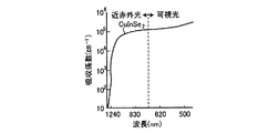
図5は、CIS薄膜(CIGS薄膜も同様である)の、光の波長に対する吸収係数を示す図である。図示するように、CIS膜(CIGS薄膜)は、可視光から近赤外光までの広範囲に渡り、高い感度をもつことがわかる。 FIG. 5 is a diagram showing the absorption coefficient of the CIS thin film (same for CIGS thin film) with respect to the wavelength of light. As shown, the CIS film (CIGS thin film) has high sensitivity over a wide range from visible light to near infrared light.
この点に着目し、本実施の形態では、本発明の化合物半導体薄膜からなる光電変換装置を、MOSトランジスタなどの形成されたシリコン基板上に積層して、複合イメージセンサを形成する。 Focusing on this point, in this embodiment, a composite image sensor is formed by stacking a photoelectric conversion device made of the compound semiconductor thin film of the present invention on a silicon substrate on which a MOS transistor or the like is formed.
図6は、通常の、シリコン基板に形成されるCMOSイメージセンサの概略断面図である。また、図7は、シリコン系のCMOS回路上に化合物半導体薄膜からなる光電変換装置(フォトセンサ)を積層してなる、本発明の複合イメージセンサの概略断面図である。 FIG. 6 is a schematic cross-sectional view of a normal CMOS image sensor formed on a silicon substrate. FIG. 7 is a schematic cross-sectional view of the composite image sensor of the present invention in which a photoelectric conversion device (photosensor) made of a compound semiconductor thin film is stacked on a silicon-based CMOS circuit.
図6に示すように通常のCMOSイメージセンサは、P−型シリコン基板600内に、フォトダイオード610(例えば、pin構造をもつ)と、MOSトランジスタを構成するn+拡散層616、618、620が形成され、また、P−型シリコン基板600上に、MOSトランジスタのゲート層612,614と、配線層622と、保護膜(層間絶縁膜を含む)624が形成されている。
As shown in FIG. 6, a normal CMOS image sensor includes a photodiode 610 (for example, having a pin structure) and n + diffusion layers 616, 618, and 620 constituting a MOS transistor in a P −
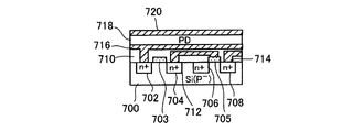
これに対し、本発明の複合イメージセンサは、P−型シリコン基板700内に、MOSトランジスタを構成するn+拡散層702、704、706,708が形成され、また、P−型シリコン基板700上に、MOSトランジスタのゲート層703,705と、配線層712,714と、層間絶縁膜710が形成されている。
In contrast, the composite image sensor of the present invention, P - -
そして、この層間絶縁膜710上に、化合物半導体薄膜からなる光電変換装置(フォトセンサ)が積層形成されている。
A photoelectric conversion device (photosensor) made of a compound semiconductor thin film is stacked on the
この光電変換装置(フォトセンサ)は、下部配線層716と、光吸収層として機能するCIGS薄膜(PD)718(図中、電極層は省略している)と、上部配線層720と、によって構成されている。
This photoelectric conversion device (photosensor) includes a
前記実施の形態で説明したように、本発明のCIGS薄膜は、フォトリソグラフィを用いた、ドライとウエットの2段エッチングによって残渣なく、高精度にパターニングされ、結晶へのダメージ、結晶欠陥が低減され、また、ZnO膜のパターニングによって、PN接合界面の端部がCIGS薄膜のエッチングされた側壁に達しないように埋め込まれており、暗電流が、従来デバイスに比べ、5桁程度、劇的に低減されている。 As described in the above embodiment, the CIGS thin film according to the present invention is patterned with high accuracy without residue by dry and wet two-step etching using photolithography, and damage to crystals and crystal defects are reduced. Also, by patterning the ZnO film, the end of the PN junction interface is embedded so as not to reach the etched side wall of the CIGS thin film, and the dark current is dramatically reduced by about five orders of magnitude compared to conventional devices. Has been.
本発明のセンサは、近赤外光にも高い感度を有するため、セキュリティカメラ(昼間は可視光をセンシングし、夜間は近赤外光をセンシングするカメラ)や、個人認証カメラ(外光の影響を受けない近赤外光で個人認証するためのカメラ)、あるいは、車載カメラ(夜間の視覚補助や遠方の視野確保等にために車に搭載されるカメラ)として、十分に利用可能である。 Since the sensor of the present invention has high sensitivity to near-infrared light, a security camera (a camera that senses visible light during the day and a near-infrared light at night) and a personal authentication camera (the influence of external light). It can be sufficiently used as a camera for personal authentication using near-infrared light that does not receive light, or a vehicle-mounted camera (a camera mounted in a car for night vision assistance or securing a far vision).
なお、上記の実施の形態では、カルコパイライト構造をもつ化合物半導体薄膜(CIGS薄膜)としては、Cu(Inx,Ga(1-x))Se2を用いているが、これに限定されるものではない。 In the above embodiment, Cu (In x , Ga (1-x) ) Se 2 is used as the compound semiconductor thin film (CIGS thin film) having a chalcopyrite structure, but the present invention is not limited to this. is not.
CIGS薄膜としては、Cu(Inx,Ga(1-x))(Sey,S(1-y))2 x=0〜1,y=0〜1という組成のものも知られており、このような組成をもつCIGS薄膜も利用可能である。 As the CIGS thin film, a composition of Cu (In x , Ga (1-x) ) (Se y , S (1-y) ) 2 x = 0 to 1, y = 0 to 1 is also known, A CIGS thin film having such a composition can also be used.
このCIGS薄膜は、真空蒸着法やスパッタ法により基板上に形成可能である。真空蒸着法を用いる場合、化合物の各成分(Cu,In,Ga,Se,S)を蒸発源として基板上に別々に蒸着させる。スパッタ法では、カルコパイライト 化合物をターゲットとして用いるか、あるいは、その各成分を別々にターゲットとして用いる。なお、カルコパイライト化合物半導体薄膜を金属基板又はガラス基板の上に形成する場合、基板を高温に加熱するため、カルコゲナイト元素(Se,S)の加熱による再蒸発が起こる。このため、カルコゲナイト元素の離脱による組成ずれが起こる場合がある。この場合は、成膜後にSe又はSの蒸気雰囲気中で400〜600℃の温度で1〜数時間程度の熱処理を行うようことにより、Se又はSを補充するのが望ましい(セレン化処理又は硫化処理)。 This CIGS thin film can be formed on a substrate by vacuum deposition or sputtering. When the vacuum deposition method is used, each component (Cu, In, Ga, Se, S) of the compound is vapor-deposited separately on the substrate as an evaporation source. In the sputtering method, a chalcopyrite compound is used as a target, or each component thereof is used as a target separately. In addition, when forming a chalcopyrite compound semiconductor thin film on a metal substrate or a glass substrate, since the substrate is heated to a high temperature, re-evaporation due to heating of the chalcogenite element (Se, S) occurs. For this reason, a composition shift may occur due to the chalcogenite element detachment. In this case, it is desirable to replenish Se or S by performing a heat treatment for about 1 to several hours at a temperature of 400 to 600 ° C. in a Se or S vapor atmosphere after film formation (selenization treatment or sulfurization). processing).
以上説明したように、本発明によれば、フォトリソグラフィによるエッチングによって、下部電極層、光吸収層として機能するカルコパイライト構造の化合物半導体薄膜、透光性電極層の各々をパターニングする手法を採用することによって、メカニカルスクライビングを行ったときのような、ダメージや欠陥が化合物半導体薄膜に生じず、暗電流の大幅な低減が可能となる。 As described above, according to the present invention, a technique of patterning each of the lower electrode layer, the compound semiconductor thin film having a chalcopyrite structure functioning as a light absorption layer, and the translucent electrode layer by etching by photolithography is employed. As a result, no damage or defect occurs in the compound semiconductor thin film as in mechanical scribing, and the dark current can be greatly reduced.
また、光吸収層については、ドライエッチングとウエットエッチングを組み合わせた2段エッチングを行うことによって、化合物半導体の結晶にダメージや欠陥を生じさせることなく、また、残渣を残さずに、高精度なパターニングを実現することができる。 In addition, the light-absorbing layer is subjected to two-stage etching that combines dry etching and wet etching, so that no damage or defects occur in the compound semiconductor crystal, and no residue remains. Can be realized.
また、ドライエッチングのエッチャントとして塩素系ガスを用いることによって、光吸収層を構成する化合物半導体薄膜を高レートでエッチングできる。また、ウエットエッチングについても、効率的かつ完全に残渣を除去することができる。 Further, by using a chlorine-based gas as an etchant for dry etching, the compound semiconductor thin film constituting the light absorption layer can be etched at a high rate. Also, with respect to wet etching, the residue can be removed efficiently and completely.
また、光吸収層となる化合物半導体薄膜として、In(インジウム)の一部をガリウムに置換したCIGS系の化合物半導体薄膜を使用し、バンド幅を広げることによって、キャリアの再結合過程を減らすことができ、暗電流を低減することができる。 In addition, a CIGS compound semiconductor thin film in which a part of In (indium) is substituted with gallium is used as a compound semiconductor thin film to be a light absorption layer, and the band recombination can reduce the carrier recombination process. And dark current can be reduced.
また、本発明の光電変換装置は、フォトリソグラフィを用いて、残渣を残さずに精度良くスクライビングされており、メカニカルエッチングを採用したときのような、ダメージや欠陥が化合物半導体の結晶に生じず、したがって、PN接合の界面に無用なエネルギー準位が生じず、暗電流の大幅な低減が可能である。 In addition, the photoelectric conversion device of the present invention is scribed with high precision without leaving a residue using photolithography, and damage and defects do not occur in the compound semiconductor crystal as when mechanical etching is employed, Therefore, useless energy levels are not generated at the interface of the PN junction, and the dark current can be greatly reduced.
すなわち、製造プロセスを変更し、デバイス構造を最適化することによって、暗電流を103のオーダで、改善することができる。また、Cu(Inx,Ga(1-x))Se2でのバンドギャップコントロールによって、暗電流を102のオーダで、低減することができる。 That is, the dark current can be improved on the order of 103 by changing the manufacturing process and optimizing the device structure. Further, the dark current can be reduced on the order of 102 by the band gap control in Cu (In x , Ga (1-x) ) Se 2 .
本発明のセンサは、近赤外光にも高い感度を有するため、セキュリティカメラ(昼間は可視光をセンシングし、夜間は近赤外光をセンシングするカメラ)や、個人認証カメラ(外光の影響を受けない近赤外光で個人認証するためのカメラ)、あるいは、車載カメラ(夜間の視覚補助や遠方の視野確保等にために車に搭載されるカメラ)として、十分に利用可能である。 Since the sensor of the present invention has high sensitivity to near-infrared light, a security camera (a camera that senses visible light during the day and a near-infrared light at night) and a personal authentication camera (the influence of external light). It can be sufficiently used as a camera for personal authentication using near-infrared light that does not receive light, or a vehicle-mounted camera (a camera mounted in a car for night vision assistance or securing a far vision).
また、本発明の光電変換は、PN接合の界面における光電変換ロスが、従来に比べて、十分に低減されているため、光により発生した電荷の収集効率が高く、光電変換効率が高い太陽電池を実現することができる。 Further, the photoelectric conversion of the present invention has a sufficiently low photoelectric conversion loss at the interface of the PN junction as compared with the conventional case, so that the collection efficiency of charges generated by light is high and the solar cell has high photoelectric conversion efficiency. Can be realized.
本発明は、化合物半導体薄膜を用いた光電変換素子の暗電流を大幅に低減できることから、セキュリティカメラや個人認証カメラ等に好適なフォトセンサ、固体撮像素子ならびに太陽電池、これらの光電変換素子の製造方法として有効である。 Since the present invention can greatly reduce the dark current of a photoelectric conversion element using a compound semiconductor thin film, it is suitable for a security camera, a personal authentication camera, etc., a photosensor, a solid-state imaging device, a solar cell, and production of these photoelectric conversion elements It is effective as a method.
10 ソーダライムガラス(SLG)
20 Mo(モリブデン)膜
30 光吸収層としてのCIGS薄膜
35 ドライエッチング後の残渣
40 CIGS薄膜エッチング用のレジストパターン
50 バッファ層としてのCdS膜
60 ZnO膜(i−ZnO,n−ZnO)
70 ZnO膜のエッチング用マスク(レジストパターン)
80 PN接合界面(空乏層の境界)
85,90 光電変換装置の引き出し電極
10 Soda lime glass (SLG)
20 Mo (molybdenum)
70 Mask for etching ZnO film (resist pattern)
80 PN junction interface (depletion layer boundary)
85,90 Lead electrode of photoelectric conversion device
Claims (8)
前記カルコパイライト構造の化合物半導体薄膜をフォトリソグラフィによってパターニングする工程を含む光電変換装置の製造方法。 A manufacturing method of a photoelectric conversion device configured by laminating a lower electrode layer, a compound semiconductor thin film having a chalcopyrite structure that functions as a light absorption layer on a substrate, and a translucent electrode layer,
A method for manufacturing a photoelectric conversion device, comprising a step of patterning the compound semiconductor thin film having a chalcopyrite structure by photolithography.
前記カルコパイライト構造の化合物半導体薄膜をパターニングする工程は、
ドライエッチングによりパターニングする第1の工程と、
この第1の工程で生じるエッチング残渣を、ウエットエッチングより除去する第2の工程と、
を含むことを特徴とする、光電変換装置の製造方法。 It is a manufacturing method of the photoelectric conversion device according to claim 1,
The step of patterning the chalcopyrite structure compound semiconductor thin film,
A first step of patterning by dry etching;
A second step of removing the etching residue generated in the first step by wet etching;
A process for producing a photoelectric conversion device, comprising:
前記第1の工程では、塩素系ガスおよび臭素系ガスをエッチャントとしてドライエッチングを行い、また、前記第2の工程では、前記カルコパイライト構造の化合物半導体薄膜を、臭素とメタノールの混合液、または、水とアンモニアの混合液で処理した後、塩酸と硝酸の混合液で処理することを特徴とする光電変換装置の製造方法。 It is a manufacturing method of the photoelectric conversion device according to claim 2,
In the first step, dry etching is performed using a chlorine-based gas and a bromine-based gas as an etchant, and in the second step, the chalcopyrite-structured compound semiconductor thin film is mixed with a mixture of bromine and methanol, or A method for producing a photoelectric conversion device, comprising: treating with a mixed solution of water and ammonia, and then treating with a mixed solution of hydrochloric acid and nitric acid.
前記カルコパイライト構造の化合物半導体薄膜は、Cu(Inx,Ga(1-x))Se2(0≦x≦1)であることを特徴とする光電変換装置の製造方法。 It is a manufacturing method of the photoelectric conversion device according to any one of claims 1 to 3,
The method for producing a photoelectric conversion device, wherein the chalcopyrite structured compound semiconductor thin film is Cu (In x , Ga (1-x) ) Se 2 (0 ≦ x ≦ 1).
前記カルコパイライト構造の化合物半導体薄膜を形成する工程は、CVD法により、Cu(Inx,Ga(1-x))Se2(0≦x≦1)薄膜を成膜する工程を含み、
前記透光性電極層を形成する工程は、前記化合物半導体薄膜上にノンドープのZnO膜を形成する工程と、前記ノンドープのZnO膜上にn+型のZnO膜、ITO膜などの透明電極膜とを形成する工程を含む光電変換装置の製造方法。 It is a manufacturing method of the photoelectric conversion device according to claim 4,
The step of forming the chalcopyrite structure compound semiconductor thin film includes a step of forming a Cu (Inx, Ga (1-x)) Se2 (0 ≦ x ≦ 1) thin film by a CVD method,
The step of forming the translucent electrode layer includes a step of forming a non-doped ZnO film on the compound semiconductor thin film, a transparent electrode film such as an n + -type ZnO film and an ITO film on the non-doped ZnO film, The manufacturing method of the photoelectric conversion apparatus including the process of forming.
前記光電変換装置は、近赤外光領域にも感度をもつフォトセンサであることを特徴とする光電変換装置。 The photoelectric conversion device according to claim 6,
The photoelectric conversion device is a photosensor having sensitivity also in a near infrared light region.
前記光電変換装置は、太陽電池であることを特徴とする光電変換装置。 The photoelectric conversion device according to claim 6,
The photoelectric conversion device is a solar cell.
Priority Applications (4)
| Application Number | Priority Date | Filing Date | Title |
|---|---|---|---|
| JP2005316789A JP2007123721A (en) | 2005-10-31 | 2005-10-31 | Method for manufacturing photoelectric conversion device and photoelectric conversion device |
| EP06822697A EP1950812A1 (en) | 2005-10-31 | 2006-10-31 | Method for manufacturing photoelectric converter and photoelectric converter |
| US12/084,281 US20090217969A1 (en) | 2005-10-31 | 2006-10-31 | Method for Manufacturing Photoelectric Converter and Photoelectric Converter |
| PCT/JP2006/321768 WO2007052668A1 (en) | 2005-10-31 | 2006-10-31 | Method for manufacturing photoelectric converter and photoelectric converter |
Applications Claiming Priority (1)
| Application Number | Priority Date | Filing Date | Title |
|---|---|---|---|
| JP2005316789A JP2007123721A (en) | 2005-10-31 | 2005-10-31 | Method for manufacturing photoelectric conversion device and photoelectric conversion device |
Publications (1)
| Publication Number | Publication Date |
|---|---|
| JP2007123721A true JP2007123721A (en) | 2007-05-17 |
Family
ID=38005821
Family Applications (1)
| Application Number | Title | Priority Date | Filing Date |
|---|---|---|---|
| JP2005316789A Pending JP2007123721A (en) | 2005-10-31 | 2005-10-31 | Method for manufacturing photoelectric conversion device and photoelectric conversion device |
Country Status (4)
| Country | Link |
|---|---|
| US (1) | US20090217969A1 (en) |
| EP (1) | EP1950812A1 (en) |
| JP (1) | JP2007123721A (en) |
| WO (1) | WO2007052668A1 (en) |
Cited By (18)
| Publication number | Priority date | Publication date | Assignee | Title |
|---|---|---|---|---|
| WO2009041657A1 (en) | 2007-09-28 | 2009-04-02 | Fujifilm Corporation | Substrate for solar cell and solar cell |
| WO2009041659A1 (en) | 2007-09-28 | 2009-04-02 | Fujifilm Corporation | Solar cell |
| WO2009041660A1 (en) | 2007-09-28 | 2009-04-02 | Fujifilm Corporation | Substrate for solar cell and solar cell |
| WO2009125688A1 (en) | 2008-04-11 | 2009-10-15 | ローム株式会社 | Photoelectric conversion device, method for manufacturing the same, and solid state imaging device |
| WO2010021342A2 (en) | 2008-08-19 | 2010-02-25 | ローム株式会社 | Camera |
| WO2010119943A1 (en) * | 2009-04-17 | 2010-10-21 | 昭和シェル石油株式会社 | Solar cell module provided with an edge space |
| WO2010119944A1 (en) * | 2009-04-17 | 2010-10-21 | 昭和シェル石油株式会社 | Method for manufacturing a solar cell module provided with an edge space |
| KR101020941B1 (en) | 2009-09-30 | 2011-03-09 | 엘지이노텍 주식회사 | Solar cell and manufacturing method thereof |
| WO2011036717A1 (en) * | 2009-09-25 | 2011-03-31 | 株式会社 東芝 | Thin film compound solar cell |
| WO2011162102A1 (en) * | 2010-06-23 | 2011-12-29 | パイオニア株式会社 | Imaging device |
| US8378444B2 (en) | 2009-05-19 | 2013-02-19 | Rohm Co., Ltd. | Photodiode and method of fabricating photodiode |
| JP2013062547A (en) * | 2009-06-19 | 2013-04-04 | Korea Electronics Telecommun | Solar cell and method of fabricating the same |
| US8901541B2 (en) | 2009-04-07 | 2014-12-02 | Rohm Co., Ltd. | Photoelectric conversion device and image pick-up device |
| US9024400B2 (en) | 2012-09-20 | 2015-05-05 | Seiko Epson Corporation | Photoelectric conversion element, method of manufacturing photoelectric conversion element, and electronic device |
| US9391103B2 (en) | 2013-08-15 | 2016-07-12 | Sony Corporation | Image pickup element and image pickup device |
| WO2016200216A1 (en) * | 2015-06-11 | 2016-12-15 | 주성엔지니어링(주) | Thin film type solar cell and manufacturing method therefor |
| US9893101B2 (en) | 2012-01-23 | 2018-02-13 | Sony Semiconductor Solutions Corporation | Solid-state image pickup unit, method of manufacturing solid-state image pickup unit, and electronic apparatus |
| US10009564B2 (en) | 2013-11-29 | 2018-06-26 | Sony Semiconductor Solutions Corporation | Solid-state image capturing element, manufacturing method therefor, and electronic device |
Families Citing this family (41)
| Publication number | Priority date | Publication date | Assignee | Title |
|---|---|---|---|---|
| US8017860B2 (en) | 2006-05-15 | 2011-09-13 | Stion Corporation | Method and structure for thin film photovoltaic materials using bulk semiconductor materials |
| US8299510B2 (en) * | 2007-02-02 | 2012-10-30 | Rohm Co., Ltd. | Solid state imaging device and fabrication method for the same |
| US8071179B2 (en) | 2007-06-29 | 2011-12-06 | Stion Corporation | Methods for infusing one or more materials into nano-voids if nanoporous or nanostructured materials |
| US8759671B2 (en) * | 2007-09-28 | 2014-06-24 | Stion Corporation | Thin film metal oxide bearing semiconductor material for single junction solar cell devices |
| US8287942B1 (en) | 2007-09-28 | 2012-10-16 | Stion Corporation | Method for manufacture of semiconductor bearing thin film material |
| US8187434B1 (en) | 2007-11-14 | 2012-05-29 | Stion Corporation | Method and system for large scale manufacture of thin film photovoltaic devices using single-chamber configuration |
| WO2009078299A1 (en) | 2007-12-19 | 2009-06-25 | Rohm Co., Ltd. | Solid-state imaging device and method for fabricating the same |
| US8642138B2 (en) | 2008-06-11 | 2014-02-04 | Stion Corporation | Processing method for cleaning sulfur entities of contact regions |
| US9087943B2 (en) | 2008-06-25 | 2015-07-21 | Stion Corporation | High efficiency photovoltaic cell and manufacturing method free of metal disulfide barrier material |
| US8003432B2 (en) | 2008-06-25 | 2011-08-23 | Stion Corporation | Consumable adhesive layer for thin film photovoltaic material |
| US7855089B2 (en) | 2008-09-10 | 2010-12-21 | Stion Corporation | Application specific solar cell and method for manufacture using thin film photovoltaic materials |
| US8236597B1 (en) | 2008-09-29 | 2012-08-07 | Stion Corporation | Bulk metal species treatment of thin film photovoltaic cell and manufacturing method |
| US8008112B1 (en) | 2008-09-29 | 2011-08-30 | Stion Corporation | Bulk chloride species treatment of thin film photovoltaic cell and manufacturing method |
| US8008110B1 (en) | 2008-09-29 | 2011-08-30 | Stion Corporation | Bulk sodium species treatment of thin film photovoltaic cell and manufacturing method |
| US8476104B1 (en) | 2008-09-29 | 2013-07-02 | Stion Corporation | Sodium species surface treatment of thin film photovoltaic cell and manufacturing method |
| US8501521B1 (en) | 2008-09-29 | 2013-08-06 | Stion Corporation | Copper species surface treatment of thin film photovoltaic cell and manufacturing method |
| US8026122B1 (en) | 2008-09-29 | 2011-09-27 | Stion Corporation | Metal species surface treatment of thin film photovoltaic cell and manufacturing method |
| US8394662B1 (en) | 2008-09-29 | 2013-03-12 | Stion Corporation | Chloride species surface treatment of thin film photovoltaic cell and manufacturing method |
| US8425739B1 (en) | 2008-09-30 | 2013-04-23 | Stion Corporation | In chamber sodium doping process and system for large scale cigs based thin film photovoltaic materials |
| US7910399B1 (en) | 2008-09-30 | 2011-03-22 | Stion Corporation | Thermal management and method for large scale processing of CIS and/or CIGS based thin films overlying glass substrates |
| US7863074B2 (en) | 2008-09-30 | 2011-01-04 | Stion Corporation | Patterning electrode materials free from berm structures for thin film photovoltaic cells |
| US7947524B2 (en) | 2008-09-30 | 2011-05-24 | Stion Corporation | Humidity control and method for thin film photovoltaic materials |
| US8383450B2 (en) | 2008-09-30 | 2013-02-26 | Stion Corporation | Large scale chemical bath system and method for cadmium sulfide processing of thin film photovoltaic materials |
| US8741689B2 (en) | 2008-10-01 | 2014-06-03 | Stion Corporation | Thermal pre-treatment process for soda lime glass substrate for thin film photovoltaic materials |
| US20110018103A1 (en) | 2008-10-02 | 2011-01-27 | Stion Corporation | System and method for transferring substrates in large scale processing of cigs and/or cis devices |
| US8003430B1 (en) | 2008-10-06 | 2011-08-23 | Stion Corporation | Sulfide species treatment of thin film photovoltaic cell and manufacturing method |
| US8435826B1 (en) | 2008-10-06 | 2013-05-07 | Stion Corporation | Bulk sulfide species treatment of thin film photovoltaic cell and manufacturing method |
| US8168463B2 (en) | 2008-10-17 | 2012-05-01 | Stion Corporation | Zinc oxide film method and structure for CIGS cell |
| US8344243B2 (en) | 2008-11-20 | 2013-01-01 | Stion Corporation | Method and structure for thin film photovoltaic cell using similar material junction |
| US8507786B1 (en) | 2009-06-27 | 2013-08-13 | Stion Corporation | Manufacturing method for patterning CIGS/CIS solar cells |
| US8398772B1 (en) | 2009-08-18 | 2013-03-19 | Stion Corporation | Method and structure for processing thin film PV cells with improved temperature uniformity |
| US8809096B1 (en) | 2009-10-22 | 2014-08-19 | Stion Corporation | Bell jar extraction tool method and apparatus for thin film photovoltaic materials |
| US8859880B2 (en) | 2010-01-22 | 2014-10-14 | Stion Corporation | Method and structure for tiling industrial thin-film solar devices |
| US8263494B2 (en) | 2010-01-25 | 2012-09-11 | Stion Corporation | Method for improved patterning accuracy for thin film photovoltaic panels |
| US9096930B2 (en) | 2010-03-29 | 2015-08-04 | Stion Corporation | Apparatus for manufacturing thin film photovoltaic devices |
| US8461061B2 (en) | 2010-07-23 | 2013-06-11 | Stion Corporation | Quartz boat method and apparatus for thin film thermal treatment |
| US8628997B2 (en) | 2010-10-01 | 2014-01-14 | Stion Corporation | Method and device for cadmium-free solar cells |
| US8998606B2 (en) | 2011-01-14 | 2015-04-07 | Stion Corporation | Apparatus and method utilizing forced convection for uniform thermal treatment of thin film devices |
| US8728200B1 (en) | 2011-01-14 | 2014-05-20 | Stion Corporation | Method and system for recycling processing gas for selenization of thin film photovoltaic materials |
| US8436445B2 (en) | 2011-08-15 | 2013-05-07 | Stion Corporation | Method of manufacture of sodium doped CIGS/CIGSS absorber layers for high efficiency photovoltaic devices |
| KR102492733B1 (en) | 2017-09-29 | 2023-01-27 | 삼성디스플레이 주식회사 | Copper plasma etching method and manufacturing method of display panel |
Citations (8)
| Publication number | Priority date | Publication date | Assignee | Title |
|---|---|---|---|---|
| JPS50152683A (en) * | 1974-05-27 | 1975-12-08 | ||
| JPH0232541A (en) * | 1988-07-22 | 1990-02-02 | Nec Corp | Selective elimination of dry etching damaged layer |
| US4909863A (en) * | 1988-07-13 | 1990-03-20 | University Of Delaware | Process for levelling film surfaces and products thereof |
| JPH0548141A (en) * | 1991-08-19 | 1993-02-26 | Dowa Mining Co Ltd | Manufacture of culnse2 photoelectric transfer element |
| JPH05234958A (en) * | 1992-02-20 | 1993-09-10 | Mitsubishi Electric Corp | Fine processing method of semiconductor material containing group 6 element |
| JP2002184783A (en) * | 2000-12-14 | 2002-06-28 | Nec Yamagata Ltd | Method for manufacturing semiconductor device |
| JP2004115356A (en) * | 2002-09-26 | 2004-04-15 | Honda Motor Co Ltd | Mechanical scribe device |
| JP2005101384A (en) * | 2003-09-26 | 2005-04-14 | Sanyo Electric Co Ltd | Photovoltaic device and manufacturing method thereof |
Family Cites Families (22)
| Publication number | Priority date | Publication date | Assignee | Title |
|---|---|---|---|---|
| US4360021A (en) * | 1981-05-06 | 1982-11-23 | Colgate-Palmolive Company | Absorbent article |
| JPH05262504A (en) * | 1991-09-27 | 1993-10-12 | Matsushita Electric Ind Co Ltd | Compound semiconductor, production of its thin film and semiconductor device using the same |
| US5356839A (en) * | 1993-04-12 | 1994-10-18 | Midwest Research Institute | Enhanced quality thin film Cu(In,Ga)Se2 for semiconductor device applications by vapor-phase recrystallization |
| US5436204A (en) * | 1993-04-12 | 1995-07-25 | Midwest Research Institute | Recrystallization method to selenization of thin-film Cu(In,Ga)Se2 for semiconductor device applications |
| JP3066944B2 (en) * | 1993-12-27 | 2000-07-17 | キヤノン株式会社 | Photoelectric conversion device, driving method thereof, and system having the same |
| JP2699921B2 (en) * | 1995-04-21 | 1998-01-19 | 日本電気株式会社 | Method for manufacturing semiconductor device |
| EP0853334B1 (en) * | 1996-06-19 | 2006-07-05 | Matsushita Electric Industrial Co., Ltd. | Optoelectronic material, devices using the same, and method for manufacturing the same |
| JPH10294531A (en) * | 1997-02-21 | 1998-11-04 | Toshiba Corp | Nitride compound semiconductor light emitting device |
| JPH11243224A (en) * | 1997-12-26 | 1999-09-07 | Canon Inc | Photovoltaic element module, method of manufacturing the same, and non-contact processing method |
| JPH11251612A (en) * | 1998-03-03 | 1999-09-17 | Canon Inc | Method for manufacturing photovoltaic element |
| JP2000091601A (en) * | 1998-09-07 | 2000-03-31 | Honda Motor Co Ltd | Solar battery |
| US6465811B1 (en) * | 1999-07-12 | 2002-10-15 | Gore Enterprise Holdings, Inc. | Low-capacitance bond pads for high speed devices |
| DE19958904C2 (en) * | 1999-12-07 | 2002-01-24 | Infineon Technologies Ag | Method of making a hard mask on a substrate |
| EP1284014A4 (en) * | 2000-04-20 | 2006-09-13 | Digirad Corp | TECHNIQUE FOR SUPPRESSING THE DRIVING CURRENT IN SEMICONDUCTOR DEVICES |
| AU5400501A (en) * | 2000-06-27 | 2002-01-03 | Canon Kabushiki Kaisha | Photovoltaic element, producing method therefor, and solar cell modules |
| JP2002026122A (en) * | 2000-07-04 | 2002-01-25 | Sony Corp | Method for manufacturing semiconductor device |
| JP4574833B2 (en) * | 2000-11-10 | 2010-11-04 | 浜松ホトニクス株式会社 | Manufacturing method of semiconductor photodetector |
| US7078351B2 (en) * | 2003-02-10 | 2006-07-18 | Taiwan Semiconductor Manufacturing Company, Ltd. | Photoresist intensive patterning and processing |
| JP2005019742A (en) * | 2003-06-26 | 2005-01-20 | Matsushita Electric Ind Co Ltd | Solar cell |
| JP2007519222A (en) * | 2003-07-11 | 2007-07-12 | コーニンクレッカ フィリップス エレクトロニクス エヌ ヴィ | Method of manufacturing a semiconductor device and apparatus for use in the method |
| KR100674986B1 (en) * | 2005-08-05 | 2007-01-29 | 삼성전자주식회사 | Image sensor and manufacturing method |
| KR100685903B1 (en) * | 2005-08-31 | 2007-02-26 | 동부일렉트로닉스 주식회사 | Manufacturing Method of Semiconductor Device |
-
2005
- 2005-10-31 JP JP2005316789A patent/JP2007123721A/en active Pending
-
2006
- 2006-10-31 US US12/084,281 patent/US20090217969A1/en not_active Abandoned
- 2006-10-31 WO PCT/JP2006/321768 patent/WO2007052668A1/en not_active Ceased
- 2006-10-31 EP EP06822697A patent/EP1950812A1/en not_active Withdrawn
Patent Citations (8)
| Publication number | Priority date | Publication date | Assignee | Title |
|---|---|---|---|---|
| JPS50152683A (en) * | 1974-05-27 | 1975-12-08 | ||
| US4909863A (en) * | 1988-07-13 | 1990-03-20 | University Of Delaware | Process for levelling film surfaces and products thereof |
| JPH0232541A (en) * | 1988-07-22 | 1990-02-02 | Nec Corp | Selective elimination of dry etching damaged layer |
| JPH0548141A (en) * | 1991-08-19 | 1993-02-26 | Dowa Mining Co Ltd | Manufacture of culnse2 photoelectric transfer element |
| JPH05234958A (en) * | 1992-02-20 | 1993-09-10 | Mitsubishi Electric Corp | Fine processing method of semiconductor material containing group 6 element |
| JP2002184783A (en) * | 2000-12-14 | 2002-06-28 | Nec Yamagata Ltd | Method for manufacturing semiconductor device |
| JP2004115356A (en) * | 2002-09-26 | 2004-04-15 | Honda Motor Co Ltd | Mechanical scribe device |
| JP2005101384A (en) * | 2003-09-26 | 2005-04-14 | Sanyo Electric Co Ltd | Photovoltaic device and manufacturing method thereof |
Cited By (40)
| Publication number | Priority date | Publication date | Assignee | Title |
|---|---|---|---|---|
| WO2009041659A1 (en) | 2007-09-28 | 2009-04-02 | Fujifilm Corporation | Solar cell |
| WO2009041660A1 (en) | 2007-09-28 | 2009-04-02 | Fujifilm Corporation | Substrate for solar cell and solar cell |
| WO2009041657A1 (en) | 2007-09-28 | 2009-04-02 | Fujifilm Corporation | Substrate for solar cell and solar cell |
| WO2009125688A1 (en) | 2008-04-11 | 2009-10-15 | ローム株式会社 | Photoelectric conversion device, method for manufacturing the same, and solid state imaging device |
| US8592933B2 (en) | 2008-04-11 | 2013-11-26 | Rohm Co., Ltd. | Photoelectric conversion device, fabrication method for the same, and solid state imaging device |
| WO2010021342A2 (en) | 2008-08-19 | 2010-02-25 | ローム株式会社 | Camera |
| US8629916B2 (en) | 2008-08-19 | 2014-01-14 | Rohm Co., Ltd. | Camera with imaging unit and imaging unit for camera |
| US9628739B2 (en) | 2009-04-07 | 2017-04-18 | Rohm Co., Ltd. | Photoelectric conversion device and image pick-up device |
| US9350957B2 (en) | 2009-04-07 | 2016-05-24 | Rohm Co., Ltd. | Photoelectric conversion device and image pick-up device |
| US8901541B2 (en) | 2009-04-07 | 2014-12-02 | Rohm Co., Ltd. | Photoelectric conversion device and image pick-up device |
| JP2016067034A (en) * | 2009-04-07 | 2016-04-28 | ローム株式会社 | Imaging device |
| CN102396074A (en) * | 2009-04-17 | 2012-03-28 | 昭和砚壳石油株式会社 | Solar cell module provided with an edge space |
| JP2010251575A (en) * | 2009-04-17 | 2010-11-04 | Showa Shell Sekiyu Kk | Solar cell module with edge space |
| US9166085B2 (en) | 2009-04-17 | 2015-10-20 | Solar Frontier K.K. | Method for manufacturing solar cell module provided with an edge space |
| US9166086B2 (en) | 2009-04-17 | 2015-10-20 | Solar Frontier K.K. | Method for manufacturing solar cell module provided with an edge space |
| WO2010119943A1 (en) * | 2009-04-17 | 2010-10-21 | 昭和シェル石油株式会社 | Solar cell module provided with an edge space |
| WO2010119944A1 (en) * | 2009-04-17 | 2010-10-21 | 昭和シェル石油株式会社 | Method for manufacturing a solar cell module provided with an edge space |
| CN102396074B (en) * | 2009-04-17 | 2014-09-17 | 昭和砚壳石油株式会社 | Solar cell module provided with an edge space |
| US8603853B2 (en) | 2009-04-17 | 2013-12-10 | Showa Shell Sekiyu K.K. | Method for manufacturing a solar cell module provided with an edge space |
| JP2010251576A (en) * | 2009-04-17 | 2010-11-04 | Showa Shell Sekiyu Kk | Method for manufacturing solar cell module with edge space |
| US8378444B2 (en) | 2009-05-19 | 2013-02-19 | Rohm Co., Ltd. | Photodiode and method of fabricating photodiode |
| US8828786B2 (en) | 2009-05-19 | 2014-09-09 | Rohm Co., Ltd. | Method of fabricating photodiode |
| JP2013062547A (en) * | 2009-06-19 | 2013-04-04 | Korea Electronics Telecommun | Solar cell and method of fabricating the same |
| WO2011036717A1 (en) * | 2009-09-25 | 2011-03-31 | 株式会社 東芝 | Thin film compound solar cell |
| JPWO2011036717A1 (en) * | 2009-09-25 | 2013-02-14 | 株式会社東芝 | Compound thin film solar cell |
| US20120227803A1 (en) * | 2009-09-25 | 2012-09-13 | Kabushiki Kaisha Toshiba | Compound thin film solar cell |
| KR101020941B1 (en) | 2009-09-30 | 2011-03-09 | 엘지이노텍 주식회사 | Solar cell and manufacturing method thereof |
| JP5481688B2 (en) * | 2010-06-23 | 2014-04-23 | パイオニア株式会社 | Imaging device |
| WO2011162102A1 (en) * | 2010-06-23 | 2011-12-29 | パイオニア株式会社 | Imaging device |
| US9893101B2 (en) | 2012-01-23 | 2018-02-13 | Sony Semiconductor Solutions Corporation | Solid-state image pickup unit, method of manufacturing solid-state image pickup unit, and electronic apparatus |
| US9024400B2 (en) | 2012-09-20 | 2015-05-05 | Seiko Epson Corporation | Photoelectric conversion element, method of manufacturing photoelectric conversion element, and electronic device |
| US9379278B2 (en) | 2012-09-20 | 2016-06-28 | Seiko Epson Corporation | Photoelectric conversion element, method of manufacturing photoelectric conversion element, and electronic device |
| US9391103B2 (en) | 2013-08-15 | 2016-07-12 | Sony Corporation | Image pickup element and image pickup device |
| US10009564B2 (en) | 2013-11-29 | 2018-06-26 | Sony Semiconductor Solutions Corporation | Solid-state image capturing element, manufacturing method therefor, and electronic device |
| US10536659B2 (en) | 2013-11-29 | 2020-01-14 | Sony Semiconductor Solutions Corporation | Solid-state image capturing element, manufacturing method therefor, and electronic device |
| WO2016200216A1 (en) * | 2015-06-11 | 2016-12-15 | 주성엔지니어링(주) | Thin film type solar cell and manufacturing method therefor |
| KR20160147101A (en) * | 2015-06-11 | 2016-12-22 | 주성엔지니어링(주) | Thin film type solar cell and method for manufacturing the same |
| CN108140681A (en) * | 2015-06-11 | 2018-06-08 | 周星工程股份有限公司 | Thin film solar cell and its manufacturing method |
| CN108140681B (en) * | 2015-06-11 | 2020-10-23 | 周星工程股份有限公司 | Thin-film solar cell and method for producing the same |
| KR102423108B1 (en) * | 2015-06-11 | 2022-07-22 | 주성엔지니어링(주) | Thin film type solar cell and method for manufacturing the same |
Also Published As
| Publication number | Publication date |
|---|---|
| US20090217969A1 (en) | 2009-09-03 |
| EP1950812A1 (en) | 2008-07-30 |
| WO2007052668A1 (en) | 2007-05-10 |
Similar Documents
| Publication | Publication Date | Title |
|---|---|---|
| JP2007123721A (en) | Method for manufacturing photoelectric conversion device and photoelectric conversion device | |
| US8299510B2 (en) | Solid state imaging device and fabrication method for the same | |
| JP2007123720A (en) | Photoelectric conversion device and manufacturing method thereof | |
| JP5536488B2 (en) | Solid-state imaging device for color | |
| US8592933B2 (en) | Photoelectric conversion device, fabrication method for the same, and solid state imaging device | |
| JP5597247B2 (en) | Solar cell and manufacturing method thereof | |
| KR101081294B1 (en) | Solar cell and method of fabricating the same | |
| US8486750B2 (en) | Solid-state imaging device and fabrication method thereof | |
| US20130037099A1 (en) | Device for generating solar power and method for manufacturing same | |
| KR101114018B1 (en) | Solar cell and method of fabricating the same | |
| US20150303330A1 (en) | Photoelectric conversion device and method for manufacturing photoelectric conversion device | |
| KR101028310B1 (en) | Solar cell and manufacturing method thereof | |
| KR101055019B1 (en) | Photovoltaic device and its manufacturing method | |
| KR101144447B1 (en) | Solar cell apparatus and method of fabricating the same | |
| KR101172178B1 (en) | Solar cell apparatus and method of fabricating the same | |
| KR101063641B1 (en) | Solar cell and manufacturing method thereof | |
| KR101081248B1 (en) | Solar cell and method of fabricating the same | |
| JP2012204504A (en) | Semiconductor ultraviolet light receiving element and method for manufacturing the same |
Legal Events
| Date | Code | Title | Description |
|---|---|---|---|
| A621 | Written request for application examination |
Free format text: JAPANESE INTERMEDIATE CODE: A621 Effective date: 20080905 |
|
| A521 | Request for written amendment filed |
Free format text: JAPANESE INTERMEDIATE CODE: A821 Effective date: 20080905 |
|
| A131 | Notification of reasons for refusal |
Free format text: JAPANESE INTERMEDIATE CODE: A131 Effective date: 20111108 |
|
| A02 | Decision of refusal |
Free format text: JAPANESE INTERMEDIATE CODE: A02 Effective date: 20120306 |