JP2007123737A - Board material and printed-circuit board - Google Patents
Board material and printed-circuit board Download PDFInfo
- Publication number
- JP2007123737A JP2007123737A JP2005317096A JP2005317096A JP2007123737A JP 2007123737 A JP2007123737 A JP 2007123737A JP 2005317096 A JP2005317096 A JP 2005317096A JP 2005317096 A JP2005317096 A JP 2005317096A JP 2007123737 A JP2007123737 A JP 2007123737A
- Authority
- JP
- Japan
- Prior art keywords
- circuit board
- substrate material
- fluororesin
- printed circuit
- increase
- Prior art date
- Legal status (The legal status is an assumption and is not a legal conclusion. Google has not performed a legal analysis and makes no representation as to the accuracy of the status listed.)
- Granted
Links
- 239000000463 material Substances 0.000 title claims abstract description 43
- 229920006231 aramid fiber Polymers 0.000 claims abstract description 27
- 239000011888 foil Substances 0.000 claims abstract description 19
- 239000004745 nonwoven fabric Substances 0.000 claims abstract description 16
- 239000006185 dispersion Substances 0.000 claims abstract description 12
- 238000000748 compression moulding Methods 0.000 claims abstract description 3
- 239000000758 substrate Substances 0.000 claims description 43
- 239000012790 adhesive layer Substances 0.000 claims description 17
- 229910052751 metal Inorganic materials 0.000 claims description 17
- 239000002184 metal Substances 0.000 claims description 17
- 239000004760 aramid Substances 0.000 claims description 10
- 229920000106 Liquid crystal polymer Polymers 0.000 claims description 9
- 239000004977 Liquid-crystal polymers (LCPs) Substances 0.000 claims description 9
- 239000004020 conductor Substances 0.000 claims description 5
- 238000004891 communication Methods 0.000 abstract description 10
- 229910000679 solder Inorganic materials 0.000 abstract description 7
- 239000011347 resin Substances 0.000 abstract description 6
- 229920005989 resin Polymers 0.000 abstract description 6
- 239000004744 fabric Substances 0.000 abstract description 3
- NBVXSUQYWXRMNV-UHFFFAOYSA-N fluoromethane Chemical compound FC NBVXSUQYWXRMNV-UHFFFAOYSA-N 0.000 abstract 3
- RYGMFSIKBFXOCR-UHFFFAOYSA-N Copper Chemical compound [Cu] RYGMFSIKBFXOCR-UHFFFAOYSA-N 0.000 description 13
- 239000011889 copper foil Substances 0.000 description 13
- XLYOFNOQVPJJNP-UHFFFAOYSA-N water Substances O XLYOFNOQVPJJNP-UHFFFAOYSA-N 0.000 description 12
- 229920001343 polytetrafluoroethylene Polymers 0.000 description 11
- 239000004810 polytetrafluoroethylene Substances 0.000 description 11
- 238000010521 absorption reaction Methods 0.000 description 9
- 230000000052 comparative effect Effects 0.000 description 5
- 238000000034 method Methods 0.000 description 5
- 229920011301 perfluoro alkoxyl alkane Polymers 0.000 description 5
- 239000002002 slurry Substances 0.000 description 5
- 230000000694 effects Effects 0.000 description 3
- 238000005259 measurement Methods 0.000 description 3
- YCKRFDGAMUMZLT-UHFFFAOYSA-N Fluorine atom Chemical compound [F] YCKRFDGAMUMZLT-UHFFFAOYSA-N 0.000 description 2
- XEEYBQQBJWHFJM-UHFFFAOYSA-N Iron Chemical compound [Fe] XEEYBQQBJWHFJM-UHFFFAOYSA-N 0.000 description 2
- PXHVJJICTQNCMI-UHFFFAOYSA-N Nickel Chemical compound [Ni] PXHVJJICTQNCMI-UHFFFAOYSA-N 0.000 description 2
- 229920000561 Twaron Polymers 0.000 description 2
- 238000009835 boiling Methods 0.000 description 2
- 239000011248 coating agent Substances 0.000 description 2
- 238000000576 coating method Methods 0.000 description 2
- 229920001577 copolymer Polymers 0.000 description 2
- 238000001035 drying Methods 0.000 description 2
- 229920000840 ethylene tetrafluoroethylene copolymer Polymers 0.000 description 2
- 239000011737 fluorine Substances 0.000 description 2
- 229910052731 fluorine Inorganic materials 0.000 description 2
- 125000001153 fluoro group Chemical group F* 0.000 description 2
- 239000011521 glass Substances 0.000 description 2
- 239000010410 layer Substances 0.000 description 2
- 238000000465 moulding Methods 0.000 description 2
- 239000004762 twaron Substances 0.000 description 2
- 229920000544 Gore-Tex Polymers 0.000 description 1
- 229910045601 alloy Inorganic materials 0.000 description 1
- 239000000956 alloy Substances 0.000 description 1
- 229910052782 aluminium Inorganic materials 0.000 description 1
- XAGFODPZIPBFFR-UHFFFAOYSA-N aluminium Chemical compound [Al] XAGFODPZIPBFFR-UHFFFAOYSA-N 0.000 description 1
- 238000004873 anchoring Methods 0.000 description 1
- 238000003490 calendering Methods 0.000 description 1
- 230000006835 compression Effects 0.000 description 1
- 238000007906 compression Methods 0.000 description 1
- 238000011156 evaluation Methods 0.000 description 1
- 230000002349 favourable effect Effects 0.000 description 1
- 238000005470 impregnation Methods 0.000 description 1
- 239000012212 insulator Substances 0.000 description 1
- 229910052742 iron Inorganic materials 0.000 description 1
- 238000000691 measurement method Methods 0.000 description 1
- 229910052759 nickel Inorganic materials 0.000 description 1
- 229920013653 perfluoroalkoxyethylene Polymers 0.000 description 1
- 229910000498 pewter Inorganic materials 0.000 description 1
- 239000010957 pewter Substances 0.000 description 1
- 229920003023 plastic Polymers 0.000 description 1
- -1 polytetrafluoroethylene Polymers 0.000 description 1
- 230000002265 prevention Effects 0.000 description 1
- 238000005476 soldering Methods 0.000 description 1
- 239000010935 stainless steel Substances 0.000 description 1
- 229910001220 stainless steel Inorganic materials 0.000 description 1
- 239000000126 substance Substances 0.000 description 1
- 238000010998 test method Methods 0.000 description 1
Images
Landscapes
- Laminated Bodies (AREA)
- Paper (AREA)
Abstract
Description
本発明は、高周波帯域、特にミリメートル波帯域用のプリント回路やアンテナ等に用いられる基板材料及びプリント基板に関する。 The present invention relates to a substrate material and a printed circuit board used for a printed circuit and an antenna for a high frequency band, particularly a millimeter wave band.
GHz帯域の高周波帯域の周波数の用途としては、表1に示すものがあり、表1に掲げるもの以外にも、ミリメートル波レーダを用いた自動車の衝突防止システムなどでは、70GHz以上になると予想される。 Applications of frequencies in the high frequency band of the GHz band include those shown in Table 1, and in addition to those listed in Table 1, in automobile collision prevention systems using millimeter wave radar, it is expected to be 70 GHz or higher. .
上記のような高周波帯域用のプリント回路やアンテナに使用される基板にあっては、低誘電率及び低誘電正接が求められ、これらの要求を満たすガラスクロス/フッ素樹脂基板が高周波帯域用基板として多用されている。しかし、上記ガラスクロス/フッ素樹脂基板は、周波数帯域が上昇すると誘電正接が高くなり、通信損失が増大するという欠点があった。この欠点を克服すべく、本出願人は、アラミド繊維不織布にフッ素樹脂を含浸させたプリプレグを絶縁体として用いたアラミド繊維/フッ素樹脂基板を提案した(例えば、特許文献1参照)。
前記アラミド繊維/フッ素樹脂基板は、周波数帯域の上昇に対する誘電正接の上昇を抑制して通信損失を低く抑えることが可能であるが、吸水率が大きいためにハンダ耐熱性が十分とはいえなかった。
本発明はこのような事情に鑑みてなされたものであり、周波数帯域の上昇に対する誘電正接の上昇を抑制して通信損失を低く抑えるとともにハンダ耐熱性に優れた基板材料及びプリント基板を提供することを目的としている。
The aramid fiber / fluororesin substrate can suppress the increase in the dielectric loss tangent to the increase in the frequency band and suppress the communication loss to a low level. However, it cannot be said that the solder heat resistance is sufficient due to the large water absorption rate. .
The present invention has been made in view of such circumstances, and provides a substrate material and a printed circuit board that suppresses an increase in dielectric loss tangent to an increase in frequency band, suppresses communication loss, and is excellent in soldering heat resistance. It is an object.
本発明の基板材料は、アラミド繊維10〜40重量%及びフッ素樹脂60〜90重量%を含む基板材料であって、
前記アラミド繊維とフッ素樹脂のディスパージョンとの抄造物を圧縮成形させて得られた、空隙率が5%未満の不織布であることを特徴としている。
この基板材料によれば、アラミド繊維単独の不織布にフッ素樹脂を含浸させたのではなく、アラミド繊維のパルプにフッ素樹脂のディスパージョンを予め混ぜて絡めているので、アラミド繊維の1つ1つがフッ素樹脂でコーティングされており、これを不織布にしているので基板材料自体に撥水性がある。さらに、アラミド繊維とフッ素樹脂との抄造物を圧縮して不織布にしているので、この工程で空気がある程度抜けている。このため、本発明の基板材料で形成したプリント基板は空隙が少なく、加熱しても空隙に入る蒸気の量が少なくなる。これらのことから、吸水率が低くなる。また、この基板材料はアラミド繊維とフッ素樹脂とから不織布であるため、周波数帯域の上昇に対する誘電正接の上昇を抑制して通信損失を低く抑えることが可能である。
The substrate material of the present invention is a substrate material containing 10 to 40% by weight of aramid fibers and 60 to 90% by weight of a fluorine resin,
It is a non-woven fabric having a porosity of less than 5% obtained by compression molding a paper product of the aramid fiber and a fluororesin dispersion.
According to this substrate material, aramid fibers are not impregnated with a fluororesin, but a dispersion of fluororesin is pre-mixed with aramid fiber pulp, so that each aramid fiber is fluorinated. The substrate material itself has water repellency because it is coated with resin and is made of non-woven fabric. Furthermore, since the paper product of the aramid fiber and the fluororesin is compressed into a non-woven fabric, the air escapes to some extent in this step. For this reason, the printed circuit board formed with the substrate material of the present invention has few voids, and even when heated, the amount of vapor entering the voids is small. From these things, a water absorption rate becomes low. Moreover, since this substrate material is a nonwoven fabric made of aramid fibers and fluororesin, it is possible to suppress communication loss by suppressing an increase in dielectric loss tangent to an increase in frequency band.
本発明のプリント基板は、上記基板材料の少なくとも片面側に、所定の導体パターンを形成する金属箔を配してなるプリント基板であって、
前記基板材料と前記金属箔との間にフッ素樹脂接着層が形成されていることを特徴としている。
このプリント基板によれば、上記基板材料が使用されており、アラミド繊維の1つ1つをフッ素樹脂でコーティングしたもので不織布を形成しているので基板材料自体に撥水性があり、さらに、アラミド繊維とフッ素樹脂との抄造物を圧縮して空気をある程度抜いているため、プリント基板にしても空隙が少なく、加熱しても空隙に入る蒸気の量が少なくなる。これらのことから、吸水率が低くなり、また、アラミド繊維とフッ素樹脂とからなるため、周波数帯域の上昇に対する誘電正接の上昇を抑制して通信損失を低く抑えることが可能である。さらに、この基板材料と金属箔との間にフッ素樹脂接着層が形成されているので、フッ素樹脂が有するアンカー効果により金属箔とフッ素樹脂との間の密着性が改善されて、密着性のよいプリント基板が得られる。
The printed circuit board of the present invention is a printed circuit board formed by arranging a metal foil that forms a predetermined conductor pattern on at least one side of the substrate material,
A fluororesin adhesive layer is formed between the substrate material and the metal foil.
According to this printed circuit board, the above-mentioned substrate material is used, and since the nonwoven fabric is formed by coating each of the aramid fibers with a fluororesin, the substrate material itself has water repellency. Since the paper and fluororesin paper product is compressed and air is extracted to some extent, the printed circuit board has few voids, and even when heated, the amount of vapor entering the voids is small. For these reasons, the water absorption rate is low, and since the aramid fiber and the fluororesin are used, it is possible to suppress the increase in the dielectric loss tangent with respect to the increase in the frequency band and to suppress the communication loss. Furthermore, since the fluororesin adhesive layer is formed between the substrate material and the metal foil, the anchoring effect of the fluororesin improves the adhesion between the metal foil and the fluororesin, resulting in good adhesion. A printed circuit board is obtained.
また、本発明のプリント基板は、上記基板材料の少なくとも片面側に、所定の導体パターンを形成する金属箔を配してなるプリント基板であって、
前記基板材料と前記金属箔との間に液晶ポリマー接着層が形成されていることを特徴としている。
このプリント基板によれば、上記基板材料を使用しているので、吸水率が低く、また、周波数帯域の上昇に対する誘電正接の上昇を抑制して通信損失を低く抑えることが可能である。さらに、この基板材料と金属箔との間に液晶ポリマー接着層が形成されており、液晶ポリマーは30GHz以上のミリメートル波帯域における誘電正接の上昇が低いので、周波数帯域の上昇に対する誘電正接の上昇が抑制されたプリント基板が得られやすくなる。
The printed circuit board of the present invention is a printed circuit board in which a metal foil for forming a predetermined conductor pattern is arranged on at least one side of the substrate material,
A liquid crystal polymer adhesive layer is formed between the substrate material and the metal foil.
According to this printed circuit board, since the substrate material is used, the water absorption rate is low, and it is possible to suppress the communication loss by suppressing the increase of the dielectric loss tangent with respect to the increase of the frequency band. Further, a liquid crystal polymer adhesive layer is formed between the substrate material and the metal foil. Since the liquid crystal polymer has a low increase in dielectric loss tangent in the millimeter wave band of 30 GHz or higher, the increase in dielectric loss tangent with respect to the increase in frequency band is increased. A suppressed printed circuit board is easily obtained.
本発明によれば、周波数帯域の上昇に対する誘電正接の上昇を抑制して通信損失を低く抑えるとともにハンダ耐熱性に優れた基板材料及びプリント基板を得ることができる。 ADVANTAGE OF THE INVENTION According to this invention, the board | substrate material and printed circuit board excellent in solder | pewter heat resistance can be obtained while suppressing the raise of the dielectric loss tangent with respect to the raise of a frequency band, suppressing communication loss low.
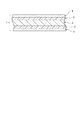
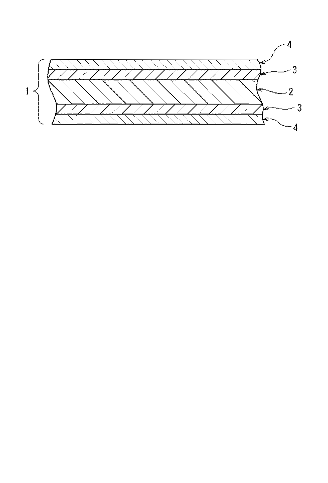
図1は、本発明の実施の形態に係るプリント基板1を示す断面図である。プリント基板1は、基板材料2の両面側に、所定の導体パターンを形成する金属箔としての銅箔4を配してなり、基板材料2と銅箔4との間にはフッ素樹脂接着層3が形成されている。なお、基板材料は1層のものが図示されているが、積層数は何層でもよい。
FIG. 1 is a cross-sectional view showing a printed circuit board 1 according to an embodiment of the present invention. The printed circuit board 1 includes
基板材料2は、アラミド繊維10〜40重量%及びフッ素樹脂60〜90重量%を含んでおり、前記アラミド繊維とフッ素樹脂のディスパージョンとの抄造物を61%以上の圧縮率で圧縮成形させて得られた、空隙率が5%未満の不織布である。
フッ素樹脂としては、ポリテトラフルオロエチレン(PTFE)が用いられるが、これ以外にも、例えば、テトラフルオロエチレン−パーフルオロアルキルビニルエーテル共重合体(PFA)、テトラフルオロエチレン−パーフルオロアルコキシエチレン共重合体(PFE)、テトラフルオロエチレン−ヘキサフルオロプロピレン共重合体(FEP)、テトラフルオロエチレン−エチレン共重合体(ETFE)を用いることができる。
As the fluororesin, polytetrafluoroethylene (PTFE) is used. Besides this, for example, tetrafluoroethylene-perfluoroalkyl vinyl ether copolymer (PFA), tetrafluoroethylene-perfluoroalkoxyethylene copolymer. (PFE), tetrafluoroethylene-hexafluoropropylene copolymer (FEP), and tetrafluoroethylene-ethylene copolymer (ETFE) can be used.
基板材料2は、アラミド繊維とフッ素樹脂とを使用し、公知の湿式抄紙法を用いて形成される。例えば、PTFEディスパージョンにアラミド繊維パルプを分散させてスラリーを調製し、このスラリーを所望の坪量に抄造し、加熱乾燥工程を経て一旦原紙とする。この原紙を密度が2.5倍以上になるように加熱加圧加工(カレンダー加工)して空隙率が5%未満の不織布を形成する。不織布の空隙が5%以上になると、吸水率が大きくなり、ハンダ耐熱性が悪くなるので好ましくない。
The
フッ素樹脂接着層3は、基板材料2と銅箔4との間に形成されており、フッ素樹脂が有するアンカー効果により銅箔4とフッ素樹脂との間の密着性が改善されることにより、密着性のよいプリント基板1が得られる。
フッ素樹脂接着層3のフッ素樹脂には、上記と同様のものを使用することができるが、ここではPFAフィルムが基板材料2に積層されて用いられている。
The fluororesin
Although the same thing as the above can be used for the fluororesin of the fluororesin
上記プリント基板1は、アラミド繊維の1つ1つをフッ素樹脂でコーティングしたものを不織布にしているので基板材料2自体に撥水性がある。さらに、この基板材料2は、アラミド繊維とフッ素樹脂との抄造物を圧縮する工程で空気がある程度抜けている。このため、この基板材料2で形成したプリント基板1は空隙が少なく、加熱しても空隙に入る蒸気の量が少ない。これらのことから、吸水率が低くなる。また、基板材料2はアラミド繊維とフッ素樹脂とから不織布である基板材料2で形成したプリント基板1は、周波数帯域の上昇に対する誘電正接の上昇を抑制して通信損失を低く抑えることが可能である。さらに、プリント基板1は、基板材料2と銅箔4との間にフッ素樹脂接着層3が形成されているので、フッ素樹脂が有するアンカー効果により銅箔4とフッ素樹脂との間の密着性が改善されて、密着性に優れる。
Since the printed board 1 is made of non-woven fabric obtained by coating each of the aramid fibers with a fluororesin, the
本発明において、前述の実施形態に限らず、本発明の範囲内で適宜変更が可能である。
金属箔としては、銅箔4を用いているが、アルミニウム、鉄、ステンレス、ニッケル等の金属又はこれらの合金の箔を使用してもかまわない。
上記実施形態では、フッ素樹脂接着層3としてPFAフィルムが基板材料2に積層されているが、フッ素樹脂フィルムを積層して接着層を形成する態様だけでなく、基板材料2にさらにフッ素樹脂、例えばPTFEを含浸させることによりフッ素樹脂接着層3を形成してもかまわない。
また、フッ素樹脂接着層3の代わりに、液晶ポリマー接着層を設けてもよい。液晶ポリマー接着層としては、液晶ポリマーからなるフィルムを使用することができる。この場合、液晶ポリマーは30GHz以上のミリメートル波帯域における誘電正接の上昇が低いので、周波数帯域の上昇に対する誘電正接の上昇が抑制されたプリント基板が得られやすくなる。
The present invention is not limited to the above-described embodiment, and can be appropriately changed within the scope of the present invention.
Although the
In the above embodiment, the PFA film is laminated on the
Further, a liquid crystal polymer adhesive layer may be provided instead of the fluororesin
(実施例1)
アラミド繊維トワロンパルプ(40重量%)とPTFEディスパージョン(三井・デュポンフロロケミカル社製PTFEディスパージョン34J)(60重量%)とを公知の湿式抄紙法を用い、例えば、アラミド繊維パルプをPTFEディスパージョンに分散させてスラリーを調製し、このスラリーを所望の坪量に抄造し、加熱乾燥工程を経て原紙とし(住友商事プラスチック(株)販売トワロンTPLシート(坪数250g/m2、厚さ0.36mm、密度0.69g/cm3)、この原紙を370℃、10.4MPaで2時間熱プレスして、厚さ0.14mm、密度1.73g/cm3、空隙率4.9%の不織布を得た。
得られた空隙率4.9%の不織布の上下面に淀川ヒューテック(株)製PFAフィルム(厚さ25μm)を配し、その上下面に銅箔(福田金属箔粉工業(株)製18μm厚銅箔CFT9LP)を配し、350℃、3MPaで1時間真空プレスして実施例1のプリント基板を作成した。
Example 1
Aramid fiber pulp (40% by weight) and PTFE dispersion (PTFE dispersion 34J manufactured by Mitsui DuPont Fluoro Chemical Co., Ltd.) (60% by weight) are used by a known wet papermaking method. For example, aramid fiber pulp is converted into PTFE dispersion. A slurry is prepared by dispersing the slurry into a desired basis weight, and the slurry is made into a desired basis weight, and is subjected to a heat-drying process to form a base paper (Twaron TPL sheet sold by Sumitomo Plastics Co., Ltd. (basis number: 250 g / m 2 , thickness: 0.36 mm) , Density 0.69 g / cm 3 ), and this base paper was hot-pressed at 370 ° C. and 10.4 MPa for 2 hours to obtain a nonwoven fabric having a thickness of 0.14 mm, a density of 1.73 g / cm 3 , and a porosity of 4.9%. Obtained.
A PFA film (thickness 25 μm) made by Yodogawa Hutec Co., Ltd. was placed on the upper and lower surfaces of the resulting non-woven fabric with a porosity of 4.9%, and copper foil (Fukuda Metal Foil Powder Co., Ltd. 18 μm thickness) was placed on the upper and lower surfaces thereof. Copper foil CFT9LP) was placed and vacuum pressed at 350 ° C. and 3 MPa for 1 hour to produce a printed circuit board of Example 1.
(実施例2)
淀川ヒューテック(株)製PFAフィルムの代わりにジャパンゴアテックス(株)製液晶ポリマーBIAC(登録商標)(厚さ25μm)を使用する以外は実施例1と同様にして実施例2のプリント基板を作成した。
(Example 2)
A printed circuit board of Example 2 was prepared in the same manner as Example 1 except that Japan Gore-Tex Co., Ltd. liquid crystal polymer BIAC (registered trademark) (thickness 25 μm) was used instead of Yodogawa Hutech Co., Ltd. PFA film. did.
(実施例3)
実施例1と同様にして得られた密度1.73g/cm3のトワロンTPLシートにダイキン(株)製PTFEディスパージョンD−70Eを含浸してPTFE比率72.8重量%のシートを得た。このシートの上下面に実施例1と同様の銅箔を配し、370℃、5MPaで4時間真空プレスして実施例3のプリント基板を作成した。
(Example 3)
A Twaron TPL sheet having a density of 1.73 g / cm 3 obtained in the same manner as in Example 1 was impregnated with PTFE dispersion D-70E manufactured by Daikin Corporation to obtain a sheet having a PTFE ratio of 72.8% by weight. The copper foil similar to Example 1 was distribute | arranged to the upper and lower surfaces of this sheet | seat, and the printed circuit board of Example 3 was created by vacuum-pressing at 370 degreeC and 5 Mpa for 4 hours.
(比較例1)
アラミド繊維の不織布(アラミド繊維ペーパー:デュポン帝人アドバンスドペーパー社製THERMOUNT#80坪数56g/m2)に、PTFEディスパージョン(三井・デュポンフロロケミカル社製PTFEディスパージョン34J)を含浸したプリプレグを4枚積層し、その上下面に銅箔(福田金属箔粉工業(株)製18μm厚銅箔CF−T9LP)を配し、熱プレス成形(成形条件:385℃、5MPa、60分間)することによって、比較例1のプリント基板を作成した。なお、比較例1のプリント基板のフッ素樹脂含浸率は、80重量%である。
(Comparative Example 1)
4 sheets of prepreg impregnated with PTFE dispersion (Mitsui / Dupont Fluoro Chemicals PTFE dispersion 34J) on an aramid fiber non-woven fabric (Aramid fiber paper: THERMOUNT # 80 manufactured by DuPont Teijin Advanced Paper Co., Ltd., 56 g / m 2 ) Then, copper foil (18 μm thick copper foil CF-T9LP manufactured by Fukuda Metal Foil Powder Co., Ltd.) was placed on the upper and lower surfaces, and hot press molding (molding conditions: 385 ° C., 5 MPa, 60 minutes) for comparison. The printed circuit board of Example 1 was produced. In addition, the fluororesin impregnation rate of the printed circuit board of Comparative Example 1 is 80% by weight.
実施例1〜3及び比較例1のプリント基板の誘電特性(誘電率及び誘電正接)、剥離強度、吸水率及び煮沸後のハンダ耐熱性の評価結果を表2に示す。なお、測定方法は、誘電率及び誘電正接については、測定周波数6、10及び12GHzでは円板共振器ストリップライン法、75GHzではファブリペロー共振器法を用いた。剥離強度、吸水率及びハンダ耐熱性については、JIS−C6481−1996(プリント配線板用銅張積層板試験方法)を使用した。 Table 2 shows the evaluation results of dielectric properties (dielectric constant and dielectric loss tangent), peel strength, water absorption, and solder heat resistance after boiling of the printed circuit boards of Examples 1 to 3 and Comparative Example 1. As the measurement method, for the dielectric constant and dielectric loss tangent, the disk resonator stripline method was used at measurement frequencies of 6, 10 and 12 GHz, and the Fabry-Perot resonator method was used at 75 GHz. For peel strength, water absorption, and solder heat resistance, JIS-C6481-1996 (a copper-clad laminate test method for printed wiring boards) was used.
表2に示すように、実施例1〜3の測定周波数6GHzにおける誘電正接に対する測定周波数75GHzにおける誘電正接の上昇比はそれぞれ2.25、2、2であり、比較例1の4と比べて小さいことから高周波帯域における通信損失を低く抑えることができる。さらに、実施例1〜3の吸水率は比較例1に比べて低く、煮沸後のハンダ耐熱性も良好である。 As shown in Table 2, the increase ratio of the dielectric loss tangent at the measurement frequency of 75 GHz with respect to the dielectric loss tangent at the measurement frequency of 6 GHz in Examples 1 to 3 is 2.25, 2 and 2, respectively, which is smaller than 4 in Comparative Example 1. Therefore, communication loss in the high frequency band can be suppressed low. Furthermore, the water absorption rate of Examples 1-3 is low compared with the comparative example 1, and the solder heat resistance after boiling is also favorable.
1 プリント基板
2 基板材料
3 フッ素樹脂接着層
4 金属箔(銅箔)
DESCRIPTION OF SYMBOLS 1 Printed
Claims (3)
前記アラミド繊維とフッ素樹脂のディスパージョンとの抄造物を圧縮成形させて得られた、空隙率が5%未満の不織布であることを特徴とする基板材料。 A substrate material comprising 10 to 40% by weight of aramid fibers and 60 to 90% by weight of a fluororesin,
A substrate material comprising a nonwoven fabric having a porosity of less than 5%, obtained by compression molding a paper product of the aramid fiber and a fluororesin dispersion.
前記基板材料と前記金属箔との間にフッ素樹脂接着層が形成されているプリント基板。 A printed circuit board comprising a metal foil for forming a predetermined conductor pattern on at least one side of the substrate material according to claim 1,
A printed circuit board in which a fluororesin adhesive layer is formed between the substrate material and the metal foil.
前記基板材料と前記金属箔との間に液晶ポリマー接着層が形成されているプリント基板。 A printed circuit board comprising a metal foil for forming a predetermined conductor pattern on at least one side of the substrate material according to claim 1,
A printed circuit board in which a liquid crystal polymer adhesive layer is formed between the substrate material and the metal foil.
Priority Applications (1)
| Application Number | Priority Date | Filing Date | Title |
|---|---|---|---|
| JP2005317096A JP4224486B2 (en) | 2005-10-31 | 2005-10-31 | Method of using printed circuit board for millimeter wave band communication |
Applications Claiming Priority (1)
| Application Number | Priority Date | Filing Date | Title |
|---|---|---|---|
| JP2005317096A JP4224486B2 (en) | 2005-10-31 | 2005-10-31 | Method of using printed circuit board for millimeter wave band communication |
Publications (2)
| Publication Number | Publication Date |
|---|---|
| JP2007123737A true JP2007123737A (en) | 2007-05-17 |
| JP4224486B2 JP4224486B2 (en) | 2009-02-12 |
Family
ID=38147218
Family Applications (1)
| Application Number | Title | Priority Date | Filing Date |
|---|---|---|---|
| JP2005317096A Expired - Fee Related JP4224486B2 (en) | 2005-10-31 | 2005-10-31 | Method of using printed circuit board for millimeter wave band communication |
Country Status (1)
| Country | Link |
|---|---|
| JP (1) | JP4224486B2 (en) |
Cited By (6)
| Publication number | Priority date | Publication date | Assignee | Title |
|---|---|---|---|---|
| JP2010274559A (en) * | 2009-05-29 | 2010-12-09 | Toyota Tsusho Corp | Paper-molded article having a functional surface layer and method for producing the same |
| WO2014054363A1 (en) * | 2012-10-02 | 2014-04-10 | 住友ベークライト株式会社 | Laminate and composite material |
| WO2014054364A1 (en) * | 2012-10-02 | 2014-04-10 | 住友ベークライト株式会社 | Article and laminate |
| JP2015008286A (en) * | 2013-05-31 | 2015-01-15 | 住友電気工業株式会社 | High frequency printed circuit board |
| WO2020059606A1 (en) * | 2018-09-18 | 2020-03-26 | Agc株式会社 | Laminate, printed board, and method for manufacturing same |
| JP2023056159A (en) * | 2021-10-07 | 2023-04-19 | 帝人株式会社 | Insulating resin material, wiring board using insulating resin material, and method for manufacturing insulating resin material |
Citations (4)
| Publication number | Priority date | Publication date | Assignee | Title |
|---|---|---|---|---|
| JPS62294545A (en) * | 1986-06-14 | 1987-12-22 | 松下電工株式会社 | Laminated board |
| JPH11112117A (en) * | 1997-10-03 | 1999-04-23 | Nippon Aramido Kk | Substrate material for printed wiring, substrate and manufacture thereof |
| JP2005501933A (en) * | 2001-08-30 | 2005-01-20 | イー・アイ・デュポン・ドウ・ヌムール・アンド・カンパニー | Solid sheet material especially useful for circuit boards |
| JP2005105165A (en) * | 2003-09-30 | 2005-04-21 | Kuraray Co Ltd | Thermoplastic liquid crystal polymer film that can be laminated at low temperature |
-
2005
- 2005-10-31 JP JP2005317096A patent/JP4224486B2/en not_active Expired - Fee Related
Patent Citations (4)
| Publication number | Priority date | Publication date | Assignee | Title |
|---|---|---|---|---|
| JPS62294545A (en) * | 1986-06-14 | 1987-12-22 | 松下電工株式会社 | Laminated board |
| JPH11112117A (en) * | 1997-10-03 | 1999-04-23 | Nippon Aramido Kk | Substrate material for printed wiring, substrate and manufacture thereof |
| JP2005501933A (en) * | 2001-08-30 | 2005-01-20 | イー・アイ・デュポン・ドウ・ヌムール・アンド・カンパニー | Solid sheet material especially useful for circuit boards |
| JP2005105165A (en) * | 2003-09-30 | 2005-04-21 | Kuraray Co Ltd | Thermoplastic liquid crystal polymer film that can be laminated at low temperature |
Cited By (7)
| Publication number | Priority date | Publication date | Assignee | Title |
|---|---|---|---|---|
| JP2010274559A (en) * | 2009-05-29 | 2010-12-09 | Toyota Tsusho Corp | Paper-molded article having a functional surface layer and method for producing the same |
| WO2014054363A1 (en) * | 2012-10-02 | 2014-04-10 | 住友ベークライト株式会社 | Laminate and composite material |
| WO2014054364A1 (en) * | 2012-10-02 | 2014-04-10 | 住友ベークライト株式会社 | Article and laminate |
| JP2015008286A (en) * | 2013-05-31 | 2015-01-15 | 住友電気工業株式会社 | High frequency printed circuit board |
| WO2020059606A1 (en) * | 2018-09-18 | 2020-03-26 | Agc株式会社 | Laminate, printed board, and method for manufacturing same |
| JP2023056159A (en) * | 2021-10-07 | 2023-04-19 | 帝人株式会社 | Insulating resin material, wiring board using insulating resin material, and method for manufacturing insulating resin material |
| JP7722893B2 (en) | 2021-10-07 | 2025-08-13 | 帝人株式会社 | Insulating resin material, wiring board using insulating resin material, and method for manufacturing insulating resin material |
Also Published As
| Publication number | Publication date |
|---|---|
| JP4224486B2 (en) | 2009-02-12 |
Similar Documents
| Publication | Publication Date | Title |
|---|---|---|
| JP4260789B2 (en) | Method of using printed circuit board for millimeter wave band communication | |
| US11818838B2 (en) | Metal-clad laminate and manufacturing method of the same | |
| US11840047B2 (en) | Metal-clad laminate, printed circuit board, and method for manufacturing the same | |
| US4640866A (en) | Printed circuit board | |
| KR100417951B1 (en) | Printed wiring board and prepreg for printed wiring board | |
| US20100000771A1 (en) | Copper-clad laminate, printed-wiring boards, multilayer printed-wiring boards, and method for manufacturing the same | |
| JPH0722741A (en) | Coverlay film and coverlay film coated circuit board | |
| WO2012161162A1 (en) | High-frequency circuit substrate | |
| JP3119577B2 (en) | Laminated board | |
| JP2013201344A (en) | Fluororesin substrate | |
| TW201632035A (en) | Antenna and electronic apparatus having antenna | |
| WO2014192322A1 (en) | High-frequency printed circuit board and wiring material | |
| JP6364184B2 (en) | Printed wiring board | |
| JP2001358415A (en) | Printed circuit board | |
| JP4224486B2 (en) | Method of using printed circuit board for millimeter wave band communication | |
| JP2020053632A (en) | Low dielectric substrate material | |
| JP3614396B2 (en) | Method of using fluororesin substrate for millimeter wave band communication and fluororesin substrate for millimeter wave band communication | |
| JP6420569B2 (en) | High frequency printed circuit board | |
| KR20050090560A (en) | Flexible copper clad laminate and its manufacturing method for high frequency | |
| JP3153511B2 (en) | Printed wiring board and method of manufacturing the same | |
| KR102360906B1 (en) | Fluorine-based substrate with a low dielectric constant | |
| JP2005273100A (en) | Fiber-made paper sheet and printed circuit board and method for producing the same | |
| JP3263173B2 (en) | Method for producing resin laminate and method for producing metal-clad laminate | |
| JP2001358416A (en) | Printed circuit board | |
| JPH05291711A (en) | Board for high-frequency circuit use |
Legal Events
| Date | Code | Title | Description |
|---|---|---|---|
| A131 | Notification of reasons for refusal |
Free format text: JAPANESE INTERMEDIATE CODE: A131 Effective date: 20080812 |
|
| A521 | Written amendment |
Free format text: JAPANESE INTERMEDIATE CODE: A523 Effective date: 20081009 |
|
| TRDD | Decision of grant or rejection written | ||
| A01 | Written decision to grant a patent or to grant a registration (utility model) |
Free format text: JAPANESE INTERMEDIATE CODE: A01 Effective date: 20081104 |
|
| A01 | Written decision to grant a patent or to grant a registration (utility model) |
Free format text: JAPANESE INTERMEDIATE CODE: A01 |
|
| A61 | First payment of annual fees (during grant procedure) |
Free format text: JAPANESE INTERMEDIATE CODE: A61 Effective date: 20081121 |
|
| R150 | Certificate of patent or registration of utility model |
Free format text: JAPANESE INTERMEDIATE CODE: R150 |
|
| FPAY | Renewal fee payment (event date is renewal date of database) |
Free format text: PAYMENT UNTIL: 20111128 Year of fee payment: 3 |
|
| LAPS | Cancellation because of no payment of annual fees |