JP2007123786A - Sheet substrate - Google Patents
Sheet substrate Download PDFInfo
- Publication number
- JP2007123786A JP2007123786A JP2005317676A JP2005317676A JP2007123786A JP 2007123786 A JP2007123786 A JP 2007123786A JP 2005317676 A JP2005317676 A JP 2005317676A JP 2005317676 A JP2005317676 A JP 2005317676A JP 2007123786 A JP2007123786 A JP 2007123786A
- Authority
- JP
- Japan
- Prior art keywords
- sheet substrate
- substrate
- positioning
- notch
- sheet
- Prior art date
- Legal status (The legal status is an assumption and is not a legal conclusion. Google has not performed a legal analysis and makes no representation as to the accuracy of the status listed.)
- Pending
Links
Images

Landscapes
- Production Of Multi-Layered Print Wiring Board (AREA)
- Structure Of Printed Boards (AREA)
Abstract
【課題】その目的は、シート基板をX方向及びθ方向共に正確に位置決めすることができるとともに、位置決めピンが該切り欠き部に接触することによるクラックが発生することのない切り欠き部を有するシート基板を提供することにある。
【解決手段】マトリクス状に配列された複数個の基板領域を有するシート基板で、該シート基板の外周に設けられた捨代領域に位置決め用の切り欠き部を形成して成るシート基板において、該位置決め用の切り欠き部が、略V字形状であり前記V字形状を構成する該シート基板の外周側面角部全てに曲率rを設けることで課題を解決するものである。
【選択図】図4An object of the present invention is to provide a sheet having a notch that can accurately position a sheet substrate in both the X direction and the θ direction, and that does not cause cracks due to the positioning pins coming into contact with the notch. It is to provide a substrate.
A sheet substrate having a plurality of substrate regions arranged in a matrix, wherein a notch for positioning is formed in an abandoned region provided on an outer periphery of the sheet substrate. The positioning notch is substantially V-shaped, and the problem is solved by providing curvature r at all the outer peripheral side corners of the sheet substrate constituting the V-shape.
[Selection] Figure 4
Description
本発明は、携帯用通信機器や電子計算機等の電子機器に用いられる水晶振動子等の圧電デバイスで用いられるシート基板に関するものである。 The present invention relates to a sheet substrate used in a piezoelectric device such as a crystal resonator used in an electronic device such as a portable communication device or an electronic computer.
複数のセラミック層を積層して成るシート基板は、例えば半導体素子や水晶振動子等の電子部品を搭載するための配線基板として使用されている。
シート基板は、電子部品が搭載される多数の基板領域がマトリクス状に形成された多数個取りの配線基板である。
A sheet substrate formed by laminating a plurality of ceramic layers is used as a wiring substrate for mounting electronic components such as semiconductor elements and crystal resonators.
The sheet substrate is a multi-piece wiring substrate in which a large number of substrate regions on which electronic components are mounted are formed in a matrix.
このシート基板の外周の捨代領域には位置決め用の切り欠き部を有している。切り欠き部は、シート基板に種々の加工を施す際や電子部品を搭載する際等にシート基板を所定の位置に位置決めするためのものであり、各辺に2箇所ずつ設けられている。そして、シート基板の位置決めは、各切り欠き部に対応する位置に位置決めピンが立設されて成る治具を準備するとともに、この治具上にシート基板を、各切り欠き部内に対応する位置決めピンが挿入されるようにして載置することによって行なわれる。(例えば、特許文献1参照。)。
しかしながら、従来のシート基板の外周に設けられた捨代領域には、円弧状の切り欠け部が設けられているが、シート基板のX方向並びにθ方向の調整が困難であるという欠点があった。また、切り欠け部が、シート基板の各辺に2箇所ずつ設けられているが、それぞれで位置合わせをする必要があるので、生産性が低下してしまうという欠点があった。 However, the ablation area provided on the outer periphery of the conventional sheet substrate is provided with an arc-shaped notch, but there is a drawback that it is difficult to adjust the X and θ directions of the sheet substrate. . Further, two cutouts are provided on each side of the sheet substrate, but there is a disadvantage that productivity is lowered because it is necessary to align each of them.
また、シート基板を多層配線基板にて形成した場合、積層がずれた場合、切り欠き部もずれてしまい位置合わせ時にくるいが生じてしまうという欠点もあった。 Further, when the sheet substrate is formed of a multilayer wiring substrate, there is a disadvantage that when the stacking is shifted, the notch portion is also shifted, and a knuckle is generated at the time of alignment.
本発明はかかる欠点に鑑み案出されたものであり、その目的は、シート基板をX方向及びθ方向共に正確に位置決めすることができるとともに、位置決めピンが該切り欠き部に接触することによるクラックが発生することのない切り欠き部を有するシート基板を提供することにある。 The present invention has been devised in view of such drawbacks, and the object thereof is to accurately position the sheet substrate in both the X direction and the θ direction, and to prevent cracks caused by the positioning pins coming into contact with the notches. It is an object of the present invention to provide a sheet substrate having a notch portion in which no occurrence occurs.
本発明のシート基板は、マトリクス状に配列された複数個の基板領域を有するシート基板で、該シート基板の外周に設けられた捨代領域に位置決め用の切り欠き部を形成して成るシート基板において、該位置決め用の切り欠き部が、略V字形状であることを特徴とするものである。 The sheet substrate of the present invention is a sheet substrate having a plurality of substrate regions arranged in a matrix, and a sheet substrate formed by forming a notch for positioning in a marginal region provided on the outer periphery of the sheet substrate. In the above, the notch for positioning is substantially V-shaped.
また本発明のシート基板は、前記シート基板が多層配線基板であり、該多層配線基板の各層に設けられている位置決め用の切り欠き部の大きさが異なることを特徴とするものである。 Further, the sheet substrate of the present invention is characterized in that the sheet substrate is a multilayer wiring substrate, and the size of the notch for positioning provided in each layer of the multilayer wiring substrate is different.
本発明のシート基板によれば、マトリクス状に配列された複数個の基板領域を有するシート基板で、該シート基板の外周に設けられた捨代領域に位置決め用の切り欠き部を形成して成るシート基板において、該位置決め用の切り欠き部が、略V字形状であることによって、ベアリングや位置決め用ピン等が接触してもクラックが発生しにくいと共に、特にX方向並びにθ方向の位置決め調整がより正確にすることが可能となる。 According to the sheet substrate of the present invention, a sheet substrate having a plurality of substrate regions arranged in a matrix form is formed by forming notch portions for positioning in a marginal region provided on the outer periphery of the sheet substrate. In the sheet substrate, the notch for positioning is substantially V-shaped, so that it is difficult for cracks to occur even when the bearings, positioning pins, etc. come into contact with each other, and in particular, positioning adjustment in the X direction and θ direction is possible. It becomes possible to make it more accurate.
また本発明のシート基板によれば、前記シート基板が多層配線基板により構成されており、該多層配線基板に設けられている位置決め用の切り欠き部の大きさが異なることによって、積層ズレが起こっても正確に位置決めすることが可能となる。 Further, according to the sheet substrate of the present invention, the sheet substrate is constituted by a multilayer wiring substrate, and stacking deviation occurs because the size of the notch for positioning provided in the multilayer wiring substrate is different. However, accurate positioning is possible.
次に、本発明のシート基板1を添付の図面を基に詳細に説明する。
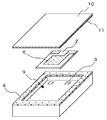
図1は本発明のシート基板1を水晶振動素子2を搭載するための多層配線基板に適用した場合の実施の形態の一例を示す斜視図である。
Next, the
FIG. 1 is a perspective view showing an example of an embodiment in which a
水晶振動素子2は、所定の結晶軸でカットした水晶片の両主面に一対の励振電極6を被着・形成してなり、外部からの変動電圧が一対の励振電極6を介して水晶片に印加されると、所定の周波数で厚みすべり振動を起こす。このような水晶振動素子2は、その両主面に被着されている励振電極6とシート基板の基板領域の対応する搭載パッド3とを導電性接着材7を介して電気的・機械的に接続することによってシート基板1の各基板領域Aのキャビティ部底面に搭載される。
The
導電性接着剤7は、シリコン樹脂やポリイミド樹脂等から成る樹脂材料中にAg等から成る導電性粒子を所定量、添加・混合してなるものである。 The conductive adhesive 7 is obtained by adding and mixing a predetermined amount of conductive particles made of Ag or the like into a resin material made of silicon resin or polyimide resin.
そして更に、基板領域Aのキャビティ部9の開口周縁には、金属から成る蓋体10が取着されている。蓋体10としては、42アロイやコバール,リン青銅等を用いれば良く、その下端部をAu−Ni等の接合材11を介して導体層4にロウ付けし、蓋体10の外周部に沿ってシート基板1の基板領域Aの上面に環状に接合することによって各基板領域の上面に取着されている。
Further, a
蓋体10は、絶縁基体1とで囲まれる領域に水晶振動素子2を収容して気密封止するためのものであり、また先に述べた導体層4を介して各基板領域下面のグランド端子に電気的に接続される。よって、水晶振動子の使用時、蓋体10はグランド電位に保持されることとなり、水晶振動素子2が蓋体10のシールド効果によって外部からの不要な電気的作用、例えばノイズ等から良好に保護される。
The
前記シート基板1は、例えば、ガラス−セラミック、アルミナセラミックス等のセラミック材料からなる矩形状の平板状基板が2層積層され、さらにセラミック材料からなるマトリクス状、即ち、縦m列×横n行の行列状に配置された多数の矩形状の孔を有する基板を積層して形成されており、マトリクス状に配置された前記孔を中心に有する個々の基板領域Aには、上面側にキャビティ部底面の一対の搭載パッド3と開口周縁を囲む封止用の導体層4が被着・形成され、下面側には入出力端子やグランド端子等の外部端子5が被着・形成されている。
The
各基板領域Aは、キャビティ部9の上面に水晶振動素子2を搭載する搭載パッド3を、キャビティの上面に封止用の導体層4を有している。該搭載パッド3には水晶振動素子2が導電性接着剤7を介して固着され、導体層4には蓋体10がろう材を介して接合される。
Each substrate region A has a mounting pad 3 on which the
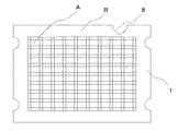
図2に示すように、マトリクス状に配された基板領域Aの間及び外周には、所定の捨代領域Bが設けられている。外周の捨代領域Bには、位置決め用の切り欠き部8が設けられている。
切り欠き部8は、シート基板1に種々の加工を施す際や水晶振動素子2を搭載する際等に、シート基板1を所定の位置に位置決めするためのものであり、この例では各辺に2箇所ずつ、それぞれセラミック層を上下に貫通して設けられている。
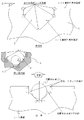
そして、図3に示すように、その切り欠き部8に位置決め用ピン12若しくはベアリングで固定することにより、X方向及びY方向、θ方向(傾き角度)の調整をすることが可能となる。
As shown in FIG. 2, predetermined spare areas B are provided between and around the substrate areas A arranged in a matrix. A
The
Then, as shown in FIG. 3, the X direction, the Y direction, and the θ direction (inclination angle) can be adjusted by fixing the
前記シート基板1のキャビティ開口面に形成されている導体層4は、タングステン(W)または、モリブデン(Mo)等から成るメタライズ層を形成し、前記メタライズ層の上面には、ニッケル(Ni)層が形成されていおり、前記ニッケル(Ni)層の上面には、金(Au)層を形成することによって構成されている。
前記メタライズ層の厚みは、10μm〜20μmであり、前記メタライズ層の上面にニッケル(Ni)層を形成し、その厚みは、8μm〜20μmである。また、前記ニッケル(Ni)層の上面には、金(Au)層が形成されており、その厚みは、0.3μm〜1.0μmである。
The conductor layer 4 formed on the cavity opening surface of the
The metallized layer has a thickness of 10 μm to 20 μm, a nickel (Ni) layer is formed on the upper surface of the metallized layer, and the thickness is 8 μm to 20 μm. Further, a gold (Au) layer is formed on the upper surface of the nickel (Ni) layer, and the thickness thereof is 0.3 μm to 1.0 μm.
また蓋体10は従来周知の金属加工法を採用し、42アロイ等の金属を所定形状に成形することによって製作され、前記蓋体10の上面には、ニッケル(Ni)層が形成され、更にニッケル(Ni)層の上面の導体層4に対応する箇所に封止材11である金錫(Au−Sn)層が形成される。金錫(Au−Sn)層の厚みは、10μm〜40μmである。例えば、成分比率が、金が80%、錫が20%のものが使用されている。
また、このような封止材11は、導体層4の凹凸を緩和し、気密性の低下を防ぐことが可能となる。また、封止材11が薄すぎると当該機能を充分に発揮しない。
Further, the
Moreover, such a sealing
位置決め用の切り欠き部8は、図4のシート基板の上面から溝部を見た拡大図に示すように略V字形状で形成され、更に前記V字形状を構成する該シート基板の外周側面角部全てに曲率rがあることによって、ベアリングや位置決め用ピン等が接触しても、角部であったりV字の頂点が無いことから、曲率rにより位置決め用ピン等が急激に接触してもクラックが発生しにくいと共に、特にX方向並びにθ方向の位置決め調整がより正確にすることが可能となる。
The
また、位置決め用切り欠き部に設けられている曲率rは、曲率半径をr1、r2し、位置決め用ピンの半径をRとしたときに、
0.50R≦r1≦0.90R
0.20≦r2≦0.40
とすることによって、位置決め精度が低下することなく、クラックを防止することが可能となる。
In addition, the curvature r provided in the positioning notch is such that the radius of curvature is r1 and r2, and the radius of the positioning pin is R.
0.50R ≦ r1 ≦ 0.90R
0.20 ≦ r2 ≦ 0.40
By doing so, it becomes possible to prevent cracks without lowering the positioning accuracy.
また、位置決め用の切り欠き部8は、各積層で切り欠きの大きさが異なることによって、積層ズレが起こっても正確に位置決めすることができる。なお、曲率rの処理方法は、基板を形成する際に打ち抜き手法を用いたり、またはヤスリを用いたりサンドブラスト手法で行うことにより形成されている。
Further, the
1・・・シート基板
2・・・水晶振動素子
3・・・搭載パッド
4・・・導体層
5・・・外部端子
6・・・励振電極
7・・・導電性接着剤
8・・・位置決め用切り欠き部
9・・・キャビティ
10・・・蓋体
11・・・封止材
12・・・位置決め用ピン
A・・・基板領域
B・・・捨代領域
DESCRIPTION OF
Claims (3)
0.50R≦r1≦0.90R
0.20≦r2≦0.40
であることを特徴とするシート基板。
The curvature r according to claim 1 is the relationship when the radius of curvature provided in the notch for positioning is r1 and r2, and the radius of the positioning pin is R.
0.50R ≦ r1 ≦ 0.90R
0.20 ≦ r2 ≦ 0.40
A sheet substrate characterized by the above.
Priority Applications (1)
| Application Number | Priority Date | Filing Date | Title |
|---|---|---|---|
| JP2005317676A JP2007123786A (en) | 2005-10-31 | 2005-10-31 | Sheet substrate |
Applications Claiming Priority (1)
| Application Number | Priority Date | Filing Date | Title |
|---|---|---|---|
| JP2005317676A JP2007123786A (en) | 2005-10-31 | 2005-10-31 | Sheet substrate |
Publications (1)
| Publication Number | Publication Date |
|---|---|
| JP2007123786A true JP2007123786A (en) | 2007-05-17 |
Family
ID=38147256
Family Applications (1)
| Application Number | Title | Priority Date | Filing Date |
|---|---|---|---|
| JP2005317676A Pending JP2007123786A (en) | 2005-10-31 | 2005-10-31 | Sheet substrate |
Country Status (1)
| Country | Link |
|---|---|
| JP (1) | JP2007123786A (en) |
Citations (6)
| Publication number | Priority date | Publication date | Assignee | Title |
|---|---|---|---|---|
| JPS61267351A (en) * | 1985-05-21 | 1986-11-26 | Kyocera Corp | Semiconductor package |
| JPS6227144A (en) * | 1985-07-29 | 1987-02-05 | 新光電気工業株式会社 | Manufacture of multilayer ceramic package |
| JPS63245945A (en) * | 1988-01-13 | 1988-10-13 | Kyocera Corp | Ceramic substrate for semiconductor package |
| JPH02138786A (en) * | 1988-08-19 | 1990-05-28 | Matsushita Electric Ind Co Ltd | Ceramic substrate for electronic components and its manufacturing method |
| JPH08264946A (en) * | 1995-03-22 | 1996-10-11 | Sumitomo Kinzoku Electro Device:Kk | Ceramic multilayer substrate and manufacturing method thereof |
| JP2000340898A (en) * | 1999-05-26 | 2000-12-08 | Kyocera Corp | Ceramic multilayer substrate |
-
2005
- 2005-10-31 JP JP2005317676A patent/JP2007123786A/en active Pending
Patent Citations (6)
| Publication number | Priority date | Publication date | Assignee | Title |
|---|---|---|---|---|
| JPS61267351A (en) * | 1985-05-21 | 1986-11-26 | Kyocera Corp | Semiconductor package |
| JPS6227144A (en) * | 1985-07-29 | 1987-02-05 | 新光電気工業株式会社 | Manufacture of multilayer ceramic package |
| JPS63245945A (en) * | 1988-01-13 | 1988-10-13 | Kyocera Corp | Ceramic substrate for semiconductor package |
| JPH02138786A (en) * | 1988-08-19 | 1990-05-28 | Matsushita Electric Ind Co Ltd | Ceramic substrate for electronic components and its manufacturing method |
| JPH08264946A (en) * | 1995-03-22 | 1996-10-11 | Sumitomo Kinzoku Electro Device:Kk | Ceramic multilayer substrate and manufacturing method thereof |
| JP2000340898A (en) * | 1999-05-26 | 2000-12-08 | Kyocera Corp | Ceramic multilayer substrate |
Similar Documents
| Publication | Publication Date | Title |
|---|---|---|
| JP5362643B2 (en) | Stacked crystal unit | |
| JP2006279872A (en) | Piezoelectric vibrator, manufacturing method thereof, and manufacturing method of piezoelectric oscillator using the piezoelectric vibrator | |
| US8056198B2 (en) | Method of manufacturing electronic device | |
| US7876168B2 (en) | Piezoelectric oscillator and method for manufacturing the same | |
| JP6017250B2 (en) | Piezoelectric device | |
| CN102201794A (en) | Electronic device and method of manufacturing electronic device | |
| CN118251839A (en) | Piezoelectric vibration element and piezoelectric device | |
| US20050225406A1 (en) | Temperature-compensated quartz-crystal oscillator | |
| JP3956614B2 (en) | Piezoelectric oscillator | |
| JP2009207068A (en) | Piezoelectric device | |
| JP4380419B2 (en) | Manufacturing method of electronic device | |
| JP4262116B2 (en) | Manufacturing method of electronic device | |
| JP2013179504A (en) | Piezoelectric device | |
| JP4724518B2 (en) | Piezoelectric oscillator | |
| JP4384546B2 (en) | Method of manufacturing electronic parts | |
| JP2005079656A (en) | Piezoelectric vibrator | |
| JP5101192B2 (en) | Piezoelectric device | |
| JP2008289055A (en) | Sheet substrate and method for manufacturing piezoelectric vibration device using sheet substrate | |
| JP2004096721A (en) | Package for piezoelectric vibrator, piezoelectric vibrator and piezoelectric device | |
| WO2020195818A1 (en) | Vibration element, vibrator, and method for manufacturing vibration element | |
| JP4113459B2 (en) | Manufacturing method of temperature compensated crystal oscillator | |
| JPH11251839A (en) | Piezo device | |
| JP4373309B2 (en) | Package for electronic components | |
| JP5005336B2 (en) | Method for manufacturing piezoelectric oscillator | |
| JP4960080B2 (en) | Piezoelectric oscillator and manufacturing method thereof |
Legal Events
| Date | Code | Title | Description |
|---|---|---|---|
| A621 | Written request for application examination |
Effective date: 20080926 Free format text: JAPANESE INTERMEDIATE CODE: A621 |
|
| A977 | Report on retrieval |
Effective date: 20100914 Free format text: JAPANESE INTERMEDIATE CODE: A971007 |
|
| A131 | Notification of reasons for refusal |
Free format text: JAPANESE INTERMEDIATE CODE: A131 Effective date: 20100921 |
|
| A02 | Decision of refusal |
Effective date: 20110201 Free format text: JAPANESE INTERMEDIATE CODE: A02 |