JP2007141876A - 半導体撮像装置及びその製造方法 - Google Patents
半導体撮像装置及びその製造方法 Download PDFInfo
- Publication number
- JP2007141876A JP2007141876A JP2005329123A JP2005329123A JP2007141876A JP 2007141876 A JP2007141876 A JP 2007141876A JP 2005329123 A JP2005329123 A JP 2005329123A JP 2005329123 A JP2005329123 A JP 2005329123A JP 2007141876 A JP2007141876 A JP 2007141876A
- Authority
- JP
- Japan
- Prior art keywords
- infrared light
- color filter
- imaging device
- filter layer
- light absorbing
- Prior art date
- Legal status (The legal status is an assumption and is not a legal conclusion. Google has not performed a legal analysis and makes no representation as to the accuracy of the status listed.)
- Pending
Links
Images


Classifications
-
- H—ELECTRICITY
- H10—SEMICONDUCTOR DEVICES; ELECTRIC SOLID-STATE DEVICES NOT OTHERWISE PROVIDED FOR
- H10F—INORGANIC SEMICONDUCTOR DEVICES SENSITIVE TO INFRARED RADIATION, LIGHT, ELECTROMAGNETIC RADIATION OF SHORTER WAVELENGTH OR CORPUSCULAR RADIATION
- H10F39/00—Integrated devices, or assemblies of multiple devices, comprising at least one element covered by group H10F30/00, e.g. radiation detectors comprising photodiode arrays
- H10F39/10—Integrated devices
- H10F39/12—Image sensors
- H10F39/15—Charge-coupled device [CCD] image sensors
- H10F39/153—Two-dimensional or three-dimensional array CCD image sensors
- H10F39/1534—Interline transfer
-
- G—PHYSICS
- G02—OPTICS
- G02B—OPTICAL ELEMENTS, SYSTEMS OR APPARATUS
- G02B5/00—Optical elements other than lenses
- G02B5/20—Filters
-
- H—ELECTRICITY
- H10—SEMICONDUCTOR DEVICES; ELECTRIC SOLID-STATE DEVICES NOT OTHERWISE PROVIDED FOR
- H10F—INORGANIC SEMICONDUCTOR DEVICES SENSITIVE TO INFRARED RADIATION, LIGHT, ELECTROMAGNETIC RADIATION OF SHORTER WAVELENGTH OR CORPUSCULAR RADIATION
- H10F39/00—Integrated devices, or assemblies of multiple devices, comprising at least one element covered by group H10F30/00, e.g. radiation detectors comprising photodiode arrays
- H10F39/80—Constructional details of image sensors
- H10F39/805—Coatings
- H10F39/8053—Colour filters
-
- G—PHYSICS
- G02—OPTICS
- G02B—OPTICAL ELEMENTS, SYSTEMS OR APPARATUS
- G02B5/00—Optical elements other than lenses
- G02B5/20—Filters
- G02B5/201—Filters in the form of arrays
-
- H—ELECTRICITY
- H10—SEMICONDUCTOR DEVICES; ELECTRIC SOLID-STATE DEVICES NOT OTHERWISE PROVIDED FOR
- H10F—INORGANIC SEMICONDUCTOR DEVICES SENSITIVE TO INFRARED RADIATION, LIGHT, ELECTROMAGNETIC RADIATION OF SHORTER WAVELENGTH OR CORPUSCULAR RADIATION
- H10F39/00—Integrated devices, or assemblies of multiple devices, comprising at least one element covered by group H10F30/00, e.g. radiation detectors comprising photodiode arrays
- H10F39/011—Manufacture or treatment of image sensors covered by group H10F39/12
- H10F39/024—Manufacture or treatment of image sensors covered by group H10F39/12 of coatings or optical elements
Landscapes
- Physics & Mathematics (AREA)
- General Physics & Mathematics (AREA)
- Optics & Photonics (AREA)
- Solid State Image Pick-Up Elements (AREA)
- Optical Filters (AREA)
- Color Television Image Signal Generators (AREA)
Abstract
【解決手段】 シリコン基板11と、受けた光を光電変換して信号電荷を出力するための複数の固体撮像素子pij及び電極を有してシリコン基板11に設けられたセンサ部20と、このセンサ部20上に設けられたカラーフィルタ層26とを備え、カラーフィルタ層は、赤外光吸収性の色素を含むものである。この構成によって、カラーフィルタ層26に赤外光カット機能を持たせることができるので、カラーフィルタ機能で要求される可視光の高透過率性に加えて、赤外光カット機能で要求される赤外光低透過率性を合わせ持った半導体撮像装置100を提供できるようになる。
【選択図】 図1
Description
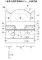
図1は本発明に係る実施形態としての半導体撮像装置100の構造例を示す一部破砕の斜視図である。
可視光吸収色素 25wt%
赤外光吸収色素 25wt%
この例で色素分散フォトレジストは、上述の材料組成比により、ネガ型フォトレジスト中にこれらの色素を添加して形成される。赤外光吸収色素材料には(1)式、すなわち、

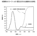
図3に示す横軸は、フィルタ透過光の波長λ[nm]である。縦軸は、カラーフィルタの透過率[%]である。図中、実線Iは本発明のカラーフィルタ(層)の分光特性である。波線IIは、比較例としての可視光吸収色素のみを適用したカラーフィルタの分光特性である。
この実施形態では、色素分散フォトレジストや色素分散樹脂に赤外吸収型色素を分散することにより、作業工程数や使用材料を増やすことなく、カラーフィルタ層26に赤外光カット機能を持たせ、所望の光学特性を得られるようにした。カラーフィルタ層26の形成方法としては、(1)色素分散フォトレジスト(顔料分散型、染料分散型)をフォトリソグラフィ技術により形成する、(2)色素分散樹脂(顔料分散型、染料分散型)をフォトリソグラフィ及びドライエッチング技術により形成する、及び、(3)透明樹脂をフォトリソグラフィで形成後、染色法で着色する等が挙げられる。
Claims (8)
- 所定の基板と、
受けた光を光電変換して信号電荷を出力するための複数の半導体撮像素子及び電極を有して前記基板に設けられた撮像素子アレイと、
前記撮像素子アレイ上に設けられたカラーフィルタ層とを備え、
前記カラーフィルタ層は、赤外光吸収性の色素を含むことを特徴とする半導体撮像装置。 - 前記赤外光吸収性の色素を含むカラーフィルタ層には、
所望のレジスト材料に可視光吸収色素材料及び赤外光吸収色素材料を所定の割合で分散させた混合物が使用されることを特徴とする請求項1に記載の半導体撮像装置。 - 前記赤外光吸収色素材料には次式、
- 前記赤外光吸収色素材料には次式、
- 所定の基板に複数の半導体撮像素子及び電極を有する撮像素子アレイを形成する工程と、
前記基板に形成された撮像素子アレイ上に、赤外光吸収性の色素を含むカラーフィルタ層を形成する工程とを有することを特徴とする半導体撮像装置の製造方法。 - 前記赤外光吸収性の色素を含むカラーフィルタ層を形成する際に、
所望のレジスト材料に可視光吸収色素材料及び赤外光吸収色素材料を所定の割合で分散させて得られる混合物を使用することを特徴とする請求項5に記載の半導体撮像装置の製造方法。 - 前記赤外光吸収色素材料には次式、
- 前記赤外光吸収色素材料には次式、
Priority Applications (7)
| Application Number | Priority Date | Filing Date | Title |
|---|---|---|---|
| JP2005329123A JP2007141876A (ja) | 2005-11-14 | 2005-11-14 | 半導体撮像装置及びその製造方法 |
| US11/542,151 US7605438B2 (en) | 2005-11-14 | 2006-10-04 | Semiconductor imaging instrument and camera |
| TW095137241A TWI365534B (en) | 2005-11-14 | 2006-10-05 | Semiconductor imaging instrument and manufacturing method thereof, and camera and manufacturing method thereof |
| KR1020060107702A KR20070051679A (ko) | 2005-11-14 | 2006-11-02 | 반도체 촬상 장치 및 그 제조 방법과 카메라 및 그 제조방법 |
| CN200610148413XA CN101183680B (zh) | 2005-11-14 | 2006-11-14 | 半导体成像装置及其制造方法和摄影机及其制造方法 |
| US12/585,476 US8093093B2 (en) | 2005-11-14 | 2009-09-16 | Semiconductor imaging instrument and manufacturing method thereof, and camera and manufacturing method thereof |
| US13/347,418 US8569854B2 (en) | 2005-11-14 | 2012-01-10 | Semiconductor imaging instrument and manufacturing method thereof, and camera and manufacturing method thereof |
Applications Claiming Priority (1)
| Application Number | Priority Date | Filing Date | Title |
|---|---|---|---|
| JP2005329123A JP2007141876A (ja) | 2005-11-14 | 2005-11-14 | 半導体撮像装置及びその製造方法 |
Publications (1)
| Publication Number | Publication Date |
|---|---|
| JP2007141876A true JP2007141876A (ja) | 2007-06-07 |
Family
ID=38040449
Family Applications (1)
| Application Number | Title | Priority Date | Filing Date |
|---|---|---|---|
| JP2005329123A Pending JP2007141876A (ja) | 2005-11-14 | 2005-11-14 | 半導体撮像装置及びその製造方法 |
Country Status (5)
| Country | Link |
|---|---|
| US (3) | US7605438B2 (ja) |
| JP (1) | JP2007141876A (ja) |
| KR (1) | KR20070051679A (ja) |
| CN (1) | CN101183680B (ja) |
| TW (1) | TWI365534B (ja) |
Cited By (9)
| Publication number | Priority date | Publication date | Assignee | Title |
|---|---|---|---|---|
| KR101038879B1 (ko) | 2009-07-28 | 2011-06-03 | 삼성전기주식회사 | 카메라 모듈 |
| WO2014061188A1 (ja) * | 2012-10-17 | 2014-04-24 | ソニー株式会社 | 撮像素子及び撮像装置 |
| WO2015079662A1 (ja) | 2013-11-26 | 2015-06-04 | ソニー株式会社 | 撮像素子 |
| WO2015115536A1 (ja) * | 2014-01-31 | 2015-08-06 | 富士フイルム株式会社 | カラーフィルタ用赤色着色組成物、着色膜、カラーフィルタ、固体撮像素子 |
| WO2015115539A1 (ja) * | 2014-01-31 | 2015-08-06 | 富士フイルム株式会社 | カラーフィルタ用緑色着色組成物、着色膜、カラーフィルタ、固体撮像素子 |
| WO2015159509A1 (en) | 2014-04-16 | 2015-10-22 | Sony Corporation | Imaging device and apparatus with infrared absorbing filter |
| WO2016186050A1 (ja) * | 2015-05-20 | 2016-11-24 | 富士フイルム株式会社 | 赤外線吸収組成物、赤外線カットフィルタ、積層体、パターン形成方法、および固体撮像素子 |
| WO2016195031A1 (ja) * | 2015-06-05 | 2016-12-08 | Jsr株式会社 | 固体撮像装置、感放射線性組成物、着色剤分散液及びカラーフィルタ |
| US11099310B2 (en) | 2015-05-27 | 2021-08-24 | Sony Corporation | Image pickup device |
Families Citing this family (10)
| Publication number | Priority date | Publication date | Assignee | Title |
|---|---|---|---|---|
| JP2006294871A (ja) * | 2005-04-11 | 2006-10-26 | Matsushita Electric Ind Co Ltd | 固体撮像装置 |
| JP5061915B2 (ja) * | 2008-01-18 | 2012-10-31 | ソニー株式会社 | 固体撮像素子及び撮像装置 |
| JP5402083B2 (ja) * | 2008-09-29 | 2014-01-29 | ソニー株式会社 | 固体撮像装置とその製造方法、及び電子機器 |
| KR20110019238A (ko) | 2009-08-19 | 2011-02-25 | 삼성전자주식회사 | 터치패널 |
| JP2012079979A (ja) * | 2010-10-04 | 2012-04-19 | Sony Corp | 固体撮像装置、および、その製造方法、電子機器 |
| EP2677364A4 (en) * | 2011-02-18 | 2015-05-13 | Adeka Corp | LIGHT-SENSITIVE COLOR COMPOSITION |
| KR101413075B1 (ko) | 2011-12-26 | 2014-06-30 | 제일모직 주식회사 | 컬러필터용 감광성 수지 조성물 및 이를 이용한 컬러필터 |
| TWI723994B (zh) * | 2015-05-22 | 2021-04-11 | 日商富士軟片股份有限公司 | 著色組成物、膜、彩色濾光片、圖案形成方法、彩色濾光片的製造方法、固體攝像元件及紅外線感測器 |
| WO2017002920A1 (ja) * | 2015-07-01 | 2017-01-05 | 日本化薬株式会社 | 有機着色顔料と赤外線吸収色素を含む顔料分散液、着色樹脂組成物および光学フィルター |
| CN111584673A (zh) * | 2020-05-22 | 2020-08-25 | 成都天马微电子有限公司 | 传感器、传感器的制造方法及电子设备 |
Citations (3)
| Publication number | Priority date | Publication date | Assignee | Title |
|---|---|---|---|---|
| JP2003222719A (ja) * | 2002-01-30 | 2003-08-08 | Toppan Printing Co Ltd | 有機顔料を用いたカラーフィルタ |
| JP2003234456A (ja) * | 2002-02-07 | 2003-08-22 | Sony Corp | 半導体撮像装置及びその製造方法 |
| JP2005223242A (ja) * | 2004-02-09 | 2005-08-18 | Toppan Printing Co Ltd | 固体撮像素子およびその製造方法 |
Family Cites Families (22)
| Publication number | Priority date | Publication date | Assignee | Title |
|---|---|---|---|---|
| JPS59229863A (ja) * | 1983-06-13 | 1984-12-24 | Oki Electric Ind Co Ltd | カラ−センサの製造方法 |
| US4808501A (en) * | 1985-10-15 | 1989-02-28 | Polaroid Corporation, Patent Dept. | Method for manufacturing an optical filter |
| US4827118A (en) * | 1986-07-10 | 1989-05-02 | Minolta Camera Kabushiki Kaisha | Light-sensitive device having color filter and manufacturing method thereof |
| JPS6373204A (ja) * | 1986-09-17 | 1988-04-02 | Mitsubishi Electric Corp | カラ−撮像素子 |
| US6383864B2 (en) | 1997-09-30 | 2002-05-07 | Siemens Aktiengesellschaft | Memory cell for dynamic random access memory (DRAM) |
| CN1295523C (zh) * | 1998-10-20 | 2007-01-17 | 富士胶片株式会社 | 滤光器 |
| JP4011766B2 (ja) * | 1998-10-20 | 2007-11-21 | 富士フイルム株式会社 | 反射防止膜 |
| US6252218B1 (en) * | 1999-02-02 | 2001-06-26 | Agilent Technologies, Inc | Amorphous silicon active pixel sensor with rectangular readout layer in a hexagonal grid layout |
| US6383894B1 (en) * | 2000-03-31 | 2002-05-07 | Intel Corporation | Method of forming scribe line planarization layer |
| JP3357030B2 (ja) * | 2000-09-01 | 2002-12-16 | 科学技術振興事業団 | 樹脂分散有機半導体膜を用いた増倍素子 |
| US20020063214A1 (en) * | 2000-11-29 | 2002-05-30 | Taiwan Semiconductor Manufacturing Co. Ltd. | Optoelectronic microelectronic fabrication with infrared filter and method for fabrication thereof |
| JP2004200360A (ja) | 2002-12-18 | 2004-07-15 | Toppan Printing Co Ltd | 固体撮像素子及びその製造方法 |
| US6818962B2 (en) * | 2002-10-25 | 2004-11-16 | Omnivision International Holding Ltd | Image sensor having integrated thin film infrared filter |
| US7524619B2 (en) * | 2002-11-22 | 2009-04-28 | Japan Carlit Co., Ltd. | Coloring matter absorbing near-infrared ray and filter for cutting off near-infrared ray |
| CN1735973A (zh) * | 2003-01-20 | 2006-02-15 | 夏普株式会社 | 用于光学传感器滤波器的透明树脂组合物、光学传感器及其制造方法 |
| JP2005026314A (ja) * | 2003-06-30 | 2005-01-27 | Sanyo Electric Co Ltd | 固体撮像素子の製造方法 |
| US7570292B2 (en) * | 2004-03-19 | 2009-08-04 | Fujifilm Corporation | Photoelectric conversion film, photoelectric conversion element, imaging element, method of applying electric field thereto and electric field-applied element |
| JP4695849B2 (ja) * | 2004-04-07 | 2011-06-08 | 富士フイルム株式会社 | 撮像センサ− |
| EP1788627A1 (en) * | 2004-06-30 | 2007-05-23 | Toppan Printing Co., Ltd. | Imaging element |
| US7329856B2 (en) * | 2004-08-24 | 2008-02-12 | Micron Technology, Inc. | Image sensor having integrated infrared-filtering optical device and related method |
| US7498123B2 (en) * | 2005-03-03 | 2009-03-03 | Exciton, Inc. | Infrared dye compositions |
| US8809876B2 (en) * | 2006-02-14 | 2014-08-19 | Massachusetts Institute Of Technology | Absorbing film |
-
2005
- 2005-11-14 JP JP2005329123A patent/JP2007141876A/ja active Pending
-
2006
- 2006-10-04 US US11/542,151 patent/US7605438B2/en active Active
- 2006-10-05 TW TW095137241A patent/TWI365534B/zh not_active IP Right Cessation
- 2006-11-02 KR KR1020060107702A patent/KR20070051679A/ko not_active Withdrawn
- 2006-11-14 CN CN200610148413XA patent/CN101183680B/zh not_active Expired - Fee Related
-
2009
- 2009-09-16 US US12/585,476 patent/US8093093B2/en not_active Expired - Fee Related
-
2012
- 2012-01-10 US US13/347,418 patent/US8569854B2/en not_active Expired - Fee Related
Patent Citations (3)
| Publication number | Priority date | Publication date | Assignee | Title |
|---|---|---|---|---|
| JP2003222719A (ja) * | 2002-01-30 | 2003-08-08 | Toppan Printing Co Ltd | 有機顔料を用いたカラーフィルタ |
| JP2003234456A (ja) * | 2002-02-07 | 2003-08-22 | Sony Corp | 半導体撮像装置及びその製造方法 |
| JP2005223242A (ja) * | 2004-02-09 | 2005-08-18 | Toppan Printing Co Ltd | 固体撮像素子およびその製造方法 |
Cited By (23)
| Publication number | Priority date | Publication date | Assignee | Title |
|---|---|---|---|---|
| KR101038879B1 (ko) | 2009-07-28 | 2011-06-03 | 삼성전기주식회사 | 카메라 모듈 |
| JPWO2014061188A1 (ja) * | 2012-10-17 | 2016-09-05 | ソニー株式会社 | 撮像素子及び撮像装置 |
| WO2014061188A1 (ja) * | 2012-10-17 | 2014-04-24 | ソニー株式会社 | 撮像素子及び撮像装置 |
| US9523803B2 (en) | 2012-10-17 | 2016-12-20 | Sony Corporation | Image capturing element and image capturing apparatus for removing infrared components from light |
| WO2015079662A1 (ja) | 2013-11-26 | 2015-06-04 | ソニー株式会社 | 撮像素子 |
| US9991304B2 (en) | 2013-11-26 | 2018-06-05 | Sony Corporation | Image pickup device having an infrared absorption layer between a laminate band-pass layer and a low refractive index layer above on-chip lenses |
| WO2015115539A1 (ja) * | 2014-01-31 | 2015-08-06 | 富士フイルム株式会社 | カラーフィルタ用緑色着色組成物、着色膜、カラーフィルタ、固体撮像素子 |
| KR20160084427A (ko) * | 2014-01-31 | 2016-07-13 | 후지필름 가부시키가이샤 | 컬러 필터용 적색 착색 조성물, 착색막, 컬러 필터, 고체 촬상 소자 |
| JP2015163955A (ja) * | 2014-01-31 | 2015-09-10 | 富士フイルム株式会社 | カラーフィルタ用赤色着色組成物、着色膜、カラーフィルタ、固体撮像素子 |
| JP2015163956A (ja) * | 2014-01-31 | 2015-09-10 | 富士フイルム株式会社 | カラーフィルタ用緑色着色組成物、着色膜、カラーフィルタ、固体撮像素子 |
| WO2015115536A1 (ja) * | 2014-01-31 | 2015-08-06 | 富士フイルム株式会社 | カラーフィルタ用赤色着色組成物、着色膜、カラーフィルタ、固体撮像素子 |
| US9740095B2 (en) | 2014-01-31 | 2017-08-22 | Fujifilm Corporation | Green coloring composition for use in color filter, colored film, color filter, and solid-state imaging device |
| KR101801671B1 (ko) * | 2014-01-31 | 2017-11-27 | 후지필름 가부시키가이샤 | 컬러 필터용 녹색 착색 조성물, 착색막, 컬러 필터, 고체 촬상 소자 |
| KR101898020B1 (ko) * | 2014-01-31 | 2018-09-12 | 후지필름 가부시키가이샤 | 컬러 필터용 적색 착색 조성물, 착색막, 컬러 필터, 고체 촬상 소자 |
| WO2015159509A1 (en) | 2014-04-16 | 2015-10-22 | Sony Corporation | Imaging device and apparatus with infrared absorbing filter |
| US10317593B2 (en) | 2014-04-16 | 2019-06-11 | Sony Corporation | Image device and imaging apparatus |
| WO2016186050A1 (ja) * | 2015-05-20 | 2016-11-24 | 富士フイルム株式会社 | 赤外線吸収組成物、赤外線カットフィルタ、積層体、パターン形成方法、および固体撮像素子 |
| JPWO2016186050A1 (ja) * | 2015-05-20 | 2018-04-19 | 富士フイルム株式会社 | 赤外線吸収組成物、赤外線カットフィルタ、積層体、パターン形成方法、および固体撮像素子 |
| US10598835B2 (en) | 2015-05-20 | 2020-03-24 | Fujifilm Corporation | Infrared absorbing composition, infrared cut filter, laminate, pattern forming method, solid image pickup element |
| US11099310B2 (en) | 2015-05-27 | 2021-08-24 | Sony Corporation | Image pickup device |
| JPWO2016195031A1 (ja) * | 2015-06-05 | 2018-03-22 | Jsr株式会社 | 固体撮像装置、感放射線性組成物、着色剤分散液及びカラーフィルタ |
| WO2016195031A1 (ja) * | 2015-06-05 | 2016-12-08 | Jsr株式会社 | 固体撮像装置、感放射線性組成物、着色剤分散液及びカラーフィルタ |
| TWI763628B (zh) * | 2015-06-05 | 2022-05-11 | 日商Jsr股份有限公司 | 固態攝影裝置、感放射線性組成物、著色劑分散液及彩色濾光片 |
Also Published As
| Publication number | Publication date |
|---|---|
| US7605438B2 (en) | 2009-10-20 |
| US8569854B2 (en) | 2013-10-29 |
| CN101183680B (zh) | 2010-05-19 |
| US20120104527A1 (en) | 2012-05-03 |
| CN101183680A (zh) | 2008-05-21 |
| TW200721476A (en) | 2007-06-01 |
| TWI365534B (en) | 2012-06-01 |
| US8093093B2 (en) | 2012-01-10 |
| US20070109548A1 (en) | 2007-05-17 |
| US20100013970A1 (en) | 2010-01-21 |
| KR20070051679A (ko) | 2007-05-18 |
Similar Documents
| Publication | Publication Date | Title |
|---|---|---|
| US8093093B2 (en) | Semiconductor imaging instrument and manufacturing method thereof, and camera and manufacturing method thereof | |
| TWI472021B (zh) | A solid-state imaging device and a method for manufacturing a solid-state imaging device, an electronic device having a solid-state imaging device | |
| JP4826111B2 (ja) | 固体撮像素子および固体撮像素子の製造方法および画像撮影装置 | |
| US9728571B2 (en) | Solid-state imaging device and method of manufacturing the same, and imaging apparatus | |
| JP4798232B2 (ja) | 固体撮像装置とその製造方法、及び電子機器 | |
| US7955764B2 (en) | Methods to make sidewall light shields for color filter array | |
| US7791659B2 (en) | Solid state imaging device and method for producing the same | |
| WO2011142065A1 (ja) | 固体撮像装置及びその製造方法 | |
| JP5725123B2 (ja) | 固体撮像装置及び電子機器 | |
| JP2010093081A (ja) | 固体撮像装置およびその製造方法 | |
| JP5360102B2 (ja) | 固体撮像装置及び電子機器 | |
| CN115176343A (zh) | 固态摄像元件和电子设备 | |
| JP2024091720A (ja) | 撮像素子 | |
| JP2003209230A (ja) | 固体撮像装置およびその製造方法 | |
| JP2011135100A (ja) | 固体撮像装置及び電子機器 | |
| JP5418527B2 (ja) | 固体撮像装置及び電子機器 | |
| CN115513230B (zh) | 图像传感器及其制作方法 | |
| JP2006278539A (ja) | Mos型固体撮像装置 | |
| JP5825398B2 (ja) | 固体撮像素子及び固体撮像素子の製造方法、電子機器 | |
| JP2008034521A (ja) | 固体撮像装置及びその製造方法 | |
| JP2003234456A (ja) | 半導体撮像装置及びその製造方法 | |
| JP2011109033A (ja) | 層内レンズおよびその製造方法、カラーフィルタおよびその製造方法、固体撮像素子およびその製造方法、並びに電子情報機器 |
Legal Events
| Date | Code | Title | Description |
|---|---|---|---|
| RD02 | Notification of acceptance of power of attorney |
Free format text: JAPANESE INTERMEDIATE CODE: A7422 Effective date: 20090904 |
|
| RD04 | Notification of resignation of power of attorney |
Free format text: JAPANESE INTERMEDIATE CODE: A7424 Effective date: 20091106 |
|
| A977 | Report on retrieval |
Free format text: JAPANESE INTERMEDIATE CODE: A971007 Effective date: 20100125 |
|
| A131 | Notification of reasons for refusal |
Free format text: JAPANESE INTERMEDIATE CODE: A131 Effective date: 20100202 |
|
| A521 | Request for written amendment filed |
Free format text: JAPANESE INTERMEDIATE CODE: A523 Effective date: 20100326 |
|
| A131 | Notification of reasons for refusal |
Free format text: JAPANESE INTERMEDIATE CODE: A131 Effective date: 20110405 |
|
| A521 | Request for written amendment filed |
Free format text: JAPANESE INTERMEDIATE CODE: A523 Effective date: 20110530 |
|
| A02 | Decision of refusal |
Free format text: JAPANESE INTERMEDIATE CODE: A02 Effective date: 20120110 |