JP2007147324A - 表面検査装置 - Google Patents
表面検査装置 Download PDFInfo
- Publication number
- JP2007147324A JP2007147324A JP2005338860A JP2005338860A JP2007147324A JP 2007147324 A JP2007147324 A JP 2007147324A JP 2005338860 A JP2005338860 A JP 2005338860A JP 2005338860 A JP2005338860 A JP 2005338860A JP 2007147324 A JP2007147324 A JP 2007147324A
- Authority
- JP
- Japan
- Prior art keywords
- light
- fiber
- inspection apparatus
- light receiving
- surface inspection
- Prior art date
- Legal status (The legal status is an assumption and is not a legal conclusion. Google has not performed a legal analysis and makes no representation as to the accuracy of the status listed.)
- Pending
Links
- 238000007689 inspection Methods 0.000 title claims abstract description 66
- 239000000835 fiber Substances 0.000 claims abstract description 70
- 230000003321 amplification Effects 0.000 claims description 9
- 238000003199 nucleic acid amplification method Methods 0.000 claims description 9
- 238000006243 chemical reaction Methods 0.000 claims description 8
- 230000007547 defect Effects 0.000 abstract description 3
- 238000000034 method Methods 0.000 description 10
- 230000003746 surface roughness Effects 0.000 description 8
- 238000005070 sampling Methods 0.000 description 7
- 238000000149 argon plasma sintering Methods 0.000 description 6
- 238000010586 diagram Methods 0.000 description 4
- 238000004364 calculation method Methods 0.000 description 3
- 230000007274 generation of a signal involved in cell-cell signaling Effects 0.000 description 3
- 238000004519 manufacturing process Methods 0.000 description 3
- XEEYBQQBJWHFJM-UHFFFAOYSA-N Iron Chemical compound [Fe] XEEYBQQBJWHFJM-UHFFFAOYSA-N 0.000 description 2
- 238000002485 combustion reaction Methods 0.000 description 2
- 239000000463 material Substances 0.000 description 2
- 230000002093 peripheral effect Effects 0.000 description 2
- 229910000838 Al alloy Inorganic materials 0.000 description 1
- 238000011109 contamination Methods 0.000 description 1
- 230000003247 decreasing effect Effects 0.000 description 1
- 230000002950 deficient Effects 0.000 description 1
- 238000001514 detection method Methods 0.000 description 1
- 238000007599 discharging Methods 0.000 description 1
- 229910052742 iron Inorganic materials 0.000 description 1
- 230000003287 optical effect Effects 0.000 description 1
- 230000011218 segmentation Effects 0.000 description 1
- 230000001360 synchronised effect Effects 0.000 description 1
Images






Landscapes
- Length Measuring Devices By Optical Means (AREA)
- Investigating Materials By The Use Of Optical Means Adapted For Particular Applications (AREA)
Abstract
【解決手段】光源24から投光ファイバ20を介して被検査物の内面に投光された光の反射光を受光ファイバ21を介して受光し、その受光量に基づいて被検査物2の表面に対応した二次元画像を生成する表面検査装置1において、前記投光ファイバ20の周囲に前記受光ファイバ21を複数配置し、且つ前記受光ファイバ21の径を前記投光ファイバ20の径よりも大きくする。
【選択図】図1
Description
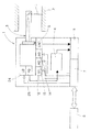
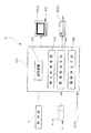
2 被検査物(円筒体,シリンダヘッド)
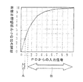
4 非線形増幅器(非線形増幅手段)
5 エンコーダ(クロック信号発生手段)
6 A/D変換部
12 回転機構(回転手段)
13 直線移動機構(直線移動手段)
20 投光ファイバ
21 受光ファイバ
30 投/受光部
46 溝幅決定手段
C 軸線
G 溝
L 光
g1 一点
g2 他点
Claims (6)
- 光源から投光ファイバを介して被検査物の表面に投光された光の反射光を受光ファイバを介して受光し、その受光量に基づいて前記被検査物の表面を検査する表面検査装置において、
前記投光ファイバの周囲に前記受光ファイバが複数配置され、且つ前記受光ファイバの径が前記投光ファイバの径よりも大きいことを特徴とする表面検査装置。 - 前記受光ファイバにより受光された光を光電変換し、光電変換後の電気信号を非線形に増幅する非線形増幅手段を備えていることを特徴とする請求項1に記載の表面検査装置。
- 前記光電変換後の信号が電圧信号であり、前記非線形増幅手段の増幅率が、低電圧部では大きく、高電圧部では小さいことを特徴とする請求項2に記載の表面検査装置。
- 前記非線形増幅手段としてログアンプを設けたことを特徴とする請求項3に記載の表面検査装置。
- 前記被検査物の前記表面が円筒体の内面であり、前記投光ファイバを介して投光される光を前記円筒体の内周に沿って回転させる回転手段と、前記円筒体の軸方向に沿って移動させる直線移動手段と、前記回転手段の回転に対応するクロック信号を発生するクロック信号発生手段と、前記増幅された電気信号を前記クロック信号と同期させてA/D変換するA/D変換手段と、を更に備えることを特徴とする請求項2〜4のいずれか1項に記載の表面検査装置。
- 前記被検査物がエンジンのシリンダヘッドであり、前記被検査物の前記表面が前記シリンダヘッドの内面であって、前記溝や傷が、前記内面に設けられた凹部の側面と前記凹部に嵌め込まれたバルブシートの側面との隙間であることを特徴とする請求項1〜5のいずれか1項に記載の表面検査装置。
Priority Applications (3)
| Application Number | Priority Date | Filing Date | Title |
|---|---|---|---|
| JP2005338860A JP2007147324A (ja) | 2005-11-24 | 2005-11-24 | 表面検査装置 |
| PCT/JP2006/322814 WO2007060873A1 (ja) | 2005-11-24 | 2006-11-16 | 表面検査装置 |
| US11/561,950 US20070132990A1 (en) | 2005-11-24 | 2006-11-21 | Surface inspection apparatus |
Applications Claiming Priority (1)
| Application Number | Priority Date | Filing Date | Title |
|---|---|---|---|
| JP2005338860A JP2007147324A (ja) | 2005-11-24 | 2005-11-24 | 表面検査装置 |
Publications (1)
| Publication Number | Publication Date |
|---|---|
| JP2007147324A true JP2007147324A (ja) | 2007-06-14 |
Family
ID=38208910
Family Applications (1)
| Application Number | Title | Priority Date | Filing Date |
|---|---|---|---|
| JP2005338860A Pending JP2007147324A (ja) | 2005-11-24 | 2005-11-24 | 表面検査装置 |
Country Status (1)
| Country | Link |
|---|---|
| JP (1) | JP2007147324A (ja) |
Cited By (4)
| Publication number | Priority date | Publication date | Assignee | Title |
|---|---|---|---|---|
| JP2011008020A (ja) * | 2009-06-25 | 2011-01-13 | Toyota Motor Corp | 孔内の検査用プローブおよび検査装置 |
| JP2012078133A (ja) * | 2010-09-30 | 2012-04-19 | Kirin Techno-System Co Ltd | 表面検査装置の検査ヘッド |
| WO2013121831A1 (ja) * | 2012-02-17 | 2013-08-22 | 株式会社日立製作所 | 微小信号検出方法及びシステム |
| WO2020235578A1 (ja) * | 2019-05-23 | 2020-11-26 | 長野オートメーション株式会社 | 検査システム |
Citations (5)
| Publication number | Priority date | Publication date | Assignee | Title |
|---|---|---|---|---|
| JPS51106488A (ja) * | 1975-03-14 | 1976-09-21 | Aisin Seiki | Hikentainonaimenkensahohoto sonosochi |
| JPH01250806A (ja) * | 1988-03-31 | 1989-10-05 | Nachi Fujikoshi Corp | 幅寸法測定方法及びその装置 |
| JPH04199505A (ja) * | 1990-11-29 | 1992-07-20 | Canon Inc | 位置合わせ装置 |
| JPH0979993A (ja) * | 1995-09-08 | 1997-03-28 | Advantest Corp | 画像処理による検査方法 |
| JPH11281582A (ja) * | 1998-03-26 | 1999-10-15 | Tb Optical Kk | 表面検査装置 |
-
2005
- 2005-11-24 JP JP2005338860A patent/JP2007147324A/ja active Pending
Patent Citations (5)
| Publication number | Priority date | Publication date | Assignee | Title |
|---|---|---|---|---|
| JPS51106488A (ja) * | 1975-03-14 | 1976-09-21 | Aisin Seiki | Hikentainonaimenkensahohoto sonosochi |
| JPH01250806A (ja) * | 1988-03-31 | 1989-10-05 | Nachi Fujikoshi Corp | 幅寸法測定方法及びその装置 |
| JPH04199505A (ja) * | 1990-11-29 | 1992-07-20 | Canon Inc | 位置合わせ装置 |
| JPH0979993A (ja) * | 1995-09-08 | 1997-03-28 | Advantest Corp | 画像処理による検査方法 |
| JPH11281582A (ja) * | 1998-03-26 | 1999-10-15 | Tb Optical Kk | 表面検査装置 |
Cited By (7)
| Publication number | Priority date | Publication date | Assignee | Title |
|---|---|---|---|---|
| JP2011008020A (ja) * | 2009-06-25 | 2011-01-13 | Toyota Motor Corp | 孔内の検査用プローブおよび検査装置 |
| JP2012078133A (ja) * | 2010-09-30 | 2012-04-19 | Kirin Techno-System Co Ltd | 表面検査装置の検査ヘッド |
| WO2013121831A1 (ja) * | 2012-02-17 | 2013-08-22 | 株式会社日立製作所 | 微小信号検出方法及びシステム |
| JPWO2013121831A1 (ja) * | 2012-02-17 | 2015-05-11 | 株式会社日立製作所 | 微小信号検出方法及びシステム |
| WO2020235578A1 (ja) * | 2019-05-23 | 2020-11-26 | 長野オートメーション株式会社 | 検査システム |
| JPWO2020235578A1 (ja) * | 2019-05-23 | 2021-10-21 | 長野オートメーション株式会社 | 検査システム |
| US11971366B2 (en) | 2019-05-23 | 2024-04-30 | Nagano Automation Co., Ltd. | Inspection system |
Similar Documents
| Publication | Publication Date | Title |
|---|---|---|
| US11105754B2 (en) | Multi-parameter inspection apparatus for monitoring of manufacturing parts | |
| US7791721B2 (en) | Surface inspection with variable digital filtering | |
| US7456948B2 (en) | Method for detecting particles and defects and inspection equipment thereof | |
| JP2009139248A (ja) | 欠陥検出光学系および欠陥検出画像処理を搭載した表面欠陥検査装置 | |
| US12017278B2 (en) | Multi-parameter inspection apparatus for monitoring of manufacturing parts using a polarization image detector | |
| US20070132990A1 (en) | Surface inspection apparatus | |
| CN112119281B (zh) | 用于检查由透明材料所制成的物件的方法及对应的检查系统 | |
| US8563958B2 (en) | Inspection apparatus and inspection method | |
| CN105051486B (zh) | 形状检查装置 | |
| JP2003329606A (ja) | 内面検査装置 | |
| JP5564807B2 (ja) | 欠陥検査装置及び欠陥検査方法 | |
| WO2004072628A1 (ja) | 欠陥検査装置及びその方法 | |
| JP5278783B1 (ja) | 欠陥検査装置、欠陥検査方法、及び欠陥検査プログラム | |
| JP2007147324A (ja) | 表面検査装置 | |
| JP2007147323A (ja) | 表面検査装置 | |
| CN111640085B (zh) | 图像处理方法和设备、检测方法和装置、存储介质 | |
| JP4597946B2 (ja) | 端部傾斜角測定方法、起伏を有する被検査物の検査方法および検査装置 | |
| JP2011209092A (ja) | 丸棒検査装置及び丸棒検査方法 | |
| JP6826893B2 (ja) | 表面検査装置、および表面検査方法 | |
| JP5367292B2 (ja) | 表面検査装置および表面検査方法 | |
| CN111316090A (zh) | 透明或半透明材料微观缺陷检测系统及方法 | |
| JP2008057983A (ja) | レンズ研磨精度評価装置及び評価方法 | |
| JP2008185356A (ja) | 丸棒検査装置及び丸棒検査方法 | |
| JPH07229832A (ja) | 表面検査方法及び装置 | |
| JP2003130806A (ja) | 表面傷等の検出方法及び装置 |
Legal Events
| Date | Code | Title | Description |
|---|---|---|---|
| A621 | Written request for application examination |
Free format text: JAPANESE INTERMEDIATE CODE: A621 Effective date: 20081120 |
|
| A521 | Written amendment |
Free format text: JAPANESE INTERMEDIATE CODE: A523 Effective date: 20090116 |
|
| A521 | Written amendment |
Free format text: JAPANESE INTERMEDIATE CODE: A523 Effective date: 20090309 |
|
| A711 | Notification of change in applicant |
Effective date: 20090416 Free format text: JAPANESE INTERMEDIATE CODE: A712 |
|
| A521 | Written amendment |
Effective date: 20090416 Free format text: JAPANESE INTERMEDIATE CODE: A821 |
|
| A131 | Notification of reasons for refusal |
Free format text: JAPANESE INTERMEDIATE CODE: A131 Effective date: 20110802 |
|
| A02 | Decision of refusal |
Effective date: 20111206 Free format text: JAPANESE INTERMEDIATE CODE: A02 |