JP2007158237A - 積層型半導体装置 - Google Patents
積層型半導体装置 Download PDFInfo
- Publication number
- JP2007158237A JP2007158237A JP2005354807A JP2005354807A JP2007158237A JP 2007158237 A JP2007158237 A JP 2007158237A JP 2005354807 A JP2005354807 A JP 2005354807A JP 2005354807 A JP2005354807 A JP 2005354807A JP 2007158237 A JP2007158237 A JP 2007158237A
- Authority
- JP
- Japan
- Prior art keywords
- semiconductor device
- signal
- stacked semiconductor
- circuit
- chip
- Prior art date
- Legal status (The legal status is an assumption and is not a legal conclusion. Google has not performed a legal analysis and makes no representation as to the accuracy of the status listed.)
- Granted
Links
Images


Classifications
-
- H—ELECTRICITY
- H10—SEMICONDUCTOR DEVICES; ELECTRIC SOLID-STATE DEVICES NOT OTHERWISE PROVIDED FOR
- H10W—GENERIC PACKAGES, INTERCONNECTIONS, CONNECTORS OR OTHER CONSTRUCTIONAL DETAILS OF DEVICES COVERED BY CLASS H10
- H10W90/00—Package configurations
-
- G—PHYSICS
- G11—INFORMATION STORAGE
- G11C—STATIC STORES
- G11C29/00—Checking stores for correct operation ; Subsequent repair; Testing stores during standby or offline operation
- G11C29/02—Detection or location of defective auxiliary circuits, e.g. defective refresh counters
- G11C29/022—Detection or location of defective auxiliary circuits, e.g. defective refresh counters in I/O circuitry
-
- G—PHYSICS
- G11—INFORMATION STORAGE
- G11C—STATIC STORES
- G11C29/00—Checking stores for correct operation ; Subsequent repair; Testing stores during standby or offline operation
- G11C29/70—Masking faults in memories by using spares or by reconfiguring
-
- G—PHYSICS
- G11—INFORMATION STORAGE
- G11C—STATIC STORES
- G11C5/00—Details of stores covered by group G11C11/00
- G11C5/02—Disposition of storage elements, e.g. in the form of a matrix array
- G11C5/04—Supports for storage elements, e.g. memory modules; Mounting or fixing of storage elements on such supports
-
- G—PHYSICS
- G11—INFORMATION STORAGE
- G11C—STATIC STORES
- G11C29/00—Checking stores for correct operation ; Subsequent repair; Testing stores during standby or offline operation
- G11C29/02—Detection or location of defective auxiliary circuits, e.g. defective refresh counters
-
- H—ELECTRICITY
- H10—SEMICONDUCTOR DEVICES; ELECTRIC SOLID-STATE DEVICES NOT OTHERWISE PROVIDED FOR
- H10W—GENERIC PACKAGES, INTERCONNECTIONS, CONNECTORS OR OTHER CONSTRUCTIONAL DETAILS OF DEVICES COVERED BY CLASS H10
- H10W20/00—Interconnections in chips, wafers or substrates
- H10W20/20—Interconnections within wafers or substrates, e.g. through-silicon vias [TSV]
-
- H—ELECTRICITY
- H10—SEMICONDUCTOR DEVICES; ELECTRIC SOLID-STATE DEVICES NOT OTHERWISE PROVIDED FOR
- H10W—GENERIC PACKAGES, INTERCONNECTIONS, CONNECTORS OR OTHER CONSTRUCTIONAL DETAILS OF DEVICES COVERED BY CLASS H10
- H10W70/00—Package substrates; Interposers; Redistribution layers [RDL]
- H10W70/01—Manufacture or treatment
- H10W70/05—Manufacture or treatment of insulating or insulated package substrates, or of interposers, or of redistribution layers
- H10W70/092—Adapting interconnections, e.g. making engineering charges, repairing
-
- H—ELECTRICITY
- H10—SEMICONDUCTOR DEVICES; ELECTRIC SOLID-STATE DEVICES NOT OTHERWISE PROVIDED FOR
- H10W—GENERIC PACKAGES, INTERCONNECTIONS, CONNECTORS OR OTHER CONSTRUCTIONAL DETAILS OF DEVICES COVERED BY CLASS H10
- H10W72/00—Interconnections or connectors in packages
- H10W72/071—Connecting or disconnecting
- H10W72/072—Connecting or disconnecting of bump connectors
- H10W72/07251—Connecting or disconnecting of bump connectors characterised by changes in properties of the bump connectors during connecting
- H10W72/07254—Connecting or disconnecting of bump connectors characterised by changes in properties of the bump connectors during connecting changes in dispositions
-
- H—ELECTRICITY
- H10—SEMICONDUCTOR DEVICES; ELECTRIC SOLID-STATE DEVICES NOT OTHERWISE PROVIDED FOR
- H10W—GENERIC PACKAGES, INTERCONNECTIONS, CONNECTORS OR OTHER CONSTRUCTIONAL DETAILS OF DEVICES COVERED BY CLASS H10
- H10W72/00—Interconnections or connectors in packages
- H10W72/20—Bump connectors, e.g. solder bumps or copper pillars; Dummy bumps; Thermal bumps
- H10W72/241—Dispositions, e.g. layouts
- H10W72/244—Dispositions, e.g. layouts relative to underlying supporting features, e.g. bond pads, RDLs or vias
-
- H—ELECTRICITY
- H10—SEMICONDUCTOR DEVICES; ELECTRIC SOLID-STATE DEVICES NOT OTHERWISE PROVIDED FOR
- H10W—GENERIC PACKAGES, INTERCONNECTIONS, CONNECTORS OR OTHER CONSTRUCTIONAL DETAILS OF DEVICES COVERED BY CLASS H10
- H10W72/00—Interconnections or connectors in packages
- H10W72/20—Bump connectors, e.g. solder bumps or copper pillars; Dummy bumps; Thermal bumps
- H10W72/241—Dispositions, e.g. layouts
- H10W72/247—Dispositions of multiple bumps
-
- H—ELECTRICITY
- H10—SEMICONDUCTOR DEVICES; ELECTRIC SOLID-STATE DEVICES NOT OTHERWISE PROVIDED FOR
- H10W—GENERIC PACKAGES, INTERCONNECTIONS, CONNECTORS OR OTHER CONSTRUCTIONAL DETAILS OF DEVICES COVERED BY CLASS H10
- H10W72/00—Interconnections or connectors in packages
- H10W72/90—Bond pads, in general
-
- H—ELECTRICITY
- H10—SEMICONDUCTOR DEVICES; ELECTRIC SOLID-STATE DEVICES NOT OTHERWISE PROVIDED FOR
- H10W—GENERIC PACKAGES, INTERCONNECTIONS, CONNECTORS OR OTHER CONSTRUCTIONAL DETAILS OF DEVICES COVERED BY CLASS H10
- H10W90/00—Package configurations
- H10W90/20—Configurations of stacked chips
- H10W90/284—Configurations of stacked chips characterised by structural arrangements for measuring or testing
-
- H—ELECTRICITY
- H10—SEMICONDUCTOR DEVICES; ELECTRIC SOLID-STATE DEVICES NOT OTHERWISE PROVIDED FOR
- H10W—GENERIC PACKAGES, INTERCONNECTIONS, CONNECTORS OR OTHER CONSTRUCTIONAL DETAILS OF DEVICES COVERED BY CLASS H10
- H10W90/00—Package configurations
- H10W90/701—Package configurations characterised by the relative positions of pads or connectors relative to package parts
- H10W90/721—Package configurations characterised by the relative positions of pads or connectors relative to package parts of bump connectors
- H10W90/722—Package configurations characterised by the relative positions of pads or connectors relative to package parts of bump connectors between stacked chips
-
- H—ELECTRICITY
- H10—SEMICONDUCTOR DEVICES; ELECTRIC SOLID-STATE DEVICES NOT OTHERWISE PROVIDED FOR
- H10W—GENERIC PACKAGES, INTERCONNECTIONS, CONNECTORS OR OTHER CONSTRUCTIONAL DETAILS OF DEVICES COVERED BY CLASS H10
- H10W90/00—Package configurations
- H10W90/701—Package configurations characterised by the relative positions of pads or connectors relative to package parts
- H10W90/721—Package configurations characterised by the relative positions of pads or connectors relative to package parts of bump connectors
- H10W90/724—Package configurations characterised by the relative positions of pads or connectors relative to package parts of bump connectors between a chip and a stacked insulating package substrate, interposer or RDL
Landscapes
- For Increasing The Reliability Of Semiconductor Memories (AREA)
- Static Random-Access Memory (AREA)
Abstract
【解決手段】接合不良救済手段として、信号経路を多重化した並列配置方式と、信号経路を予備の信号経路に切り換える接合不良救済回路を備える。信号数が少なくシリアルデータ伝送で超高速動作が要求される場合には並列配置方式を使用する。パラレルデータ伝送で信号数の多く場合には接合不良救済回路を使用する。このように1つの積層型半導体装置において複数の接合不良救済手段を使用することで最適な救済効率が得られる。
【選択図】 図5
Description
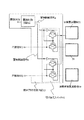
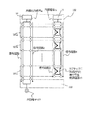
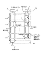
11 チップ間接合部
12 貫通電極
13 接合不良救済回路
14 内部信号生成回路
15 内部信号入出力回路
16 外部入出力回路
22、23、24、25 接合不良
30 インターポーザー上金属配線
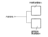
50 通常使用貫通電極
51 予備貫通電極
61 切り換えスイッチ
62 置換制御回路
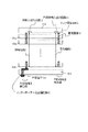
100 インターポーザー
101a、101b、101c コアチップ
102 インターフェースチップ
103 外部端子
a 外部出力信号
b、c、d 内部信号
Claims (13)
- コアチップとインターフェースチップとインターポーザーとを備えた積層型半導体装置において、前記コアチップを貫通する貫通電極と前記貫通電極間を接合したチップ間接合部から構成された信号経路に対して救済用の予備信号経路を備えた接合不良救済手段を備えたことを特徴とする積層型半導体装置。
- 前記接合不良救済手段は、前記信号経路の1本に対し前記予備信号経路を1本配置した並行配置方式であることを特徴とする請求項1に記載の積層型半導体装置。
- 前記並列配置方式は、外部から入力される信号に対し適用されたことを特徴とする請求項2に記載の積層型半導体装置。
- 前記並列配置方式は、外部端子と前記インターフェースチップとの間においてシリアルデータ伝送される信号に対し適用されたことを特徴とする請求項2に記載の積層型半導体装置。
- 前記接合不良救済手段は、前記信号経路のn(nは1以上の整数)本に対し前記予備信号経路を1本配置し、接合不良救済回路により切り換える接合不良救済回路方式であることを特徴とする請求項1に記載の積層型半導体装置。
- 前記接合不良救済回路は、前記コアチップに搭載されたことを特徴とする請求項5に記載の積層型半導体装置。
- 前記接合不良救済回路は、接合欠陥個所を記憶させておくラッチ回路と、切り換えスイッチ及び制御回路とを備えたことを特徴とする請求項6に記載の積層型半導体装置。
- 前記接合不良救済回路方式は、信号本数の多い前記インターフェースチップと前記コアチップとの間における信号に対し適用されたことを特徴とする請求項7に記載の積層型半導体装置。
- 前記接合不良救済回路方式は、前記インターフェースチップと前記コアチップとの間において、外部とやり取りされる信号をパラレル変換された信号に対し適用されたことを特徴とする請求項7に記載の積層型半導体装置。
- 前記積層型半導体装置において、前記信号経路に対し異なる接合不良救済手段が使用されたことを特徴とする請求項1に記載の積層型半導体装置。
- 前記接合不良救済手段として、外部端子との入出力回路との信号経路には並列配置方式が使用され、前記コアチップとの入出力回路との信号経路には接合不良救済回路が使用されたことを特徴とする請求項10に記載の積層型半導体装置。
- 前記コアチップにはDRAMのメモリセルとその周辺回路が搭載され、前記インターフェースチップには外部端子との外部入出力回路と前記コアチップとの内部信号入出力回路が搭載され、前記接合不良救済手段として前記外部入出力回路との信号経路には並列配置方式が使用され、前記内部信号入出力回路との信号経路には接合不良救済回路が使用されたことを特徴とする請求項10に記載の積層型半導体装置。
- 前記積層型半導体装置はバースト長2以上のデータ信号で入出力されるDDR型のDRAMであることを特徴とする請求項12に記載の積層型半導体装置。
Priority Applications (2)
| Application Number | Priority Date | Filing Date | Title |
|---|---|---|---|
| JP2005354807A JP4708176B2 (ja) | 2005-12-08 | 2005-12-08 | 半導体装置 |
| US11/635,500 US7489030B2 (en) | 2005-12-08 | 2006-12-08 | Stacked semiconductor device |
Applications Claiming Priority (1)
| Application Number | Priority Date | Filing Date | Title |
|---|---|---|---|
| JP2005354807A JP4708176B2 (ja) | 2005-12-08 | 2005-12-08 | 半導体装置 |
Publications (2)
| Publication Number | Publication Date |
|---|---|
| JP2007158237A true JP2007158237A (ja) | 2007-06-21 |
| JP4708176B2 JP4708176B2 (ja) | 2011-06-22 |
Family
ID=38138470
Family Applications (1)
| Application Number | Title | Priority Date | Filing Date |
|---|---|---|---|
| JP2005354807A Expired - Fee Related JP4708176B2 (ja) | 2005-12-08 | 2005-12-08 | 半導体装置 |
Country Status (2)
| Country | Link |
|---|---|
| US (1) | US7489030B2 (ja) |
| JP (1) | JP4708176B2 (ja) |
Cited By (34)
| Publication number | Priority date | Publication date | Assignee | Title |
|---|---|---|---|---|
| JP2010161918A (ja) * | 2009-01-06 | 2010-07-22 | O2 Micro Inc | 電池管理システム |
| JP2011503759A (ja) * | 2007-10-16 | 2011-01-27 | マイクロン テクノロジー, インク. | 積み重ねられた半導体素子用の再構成可能な接続部 |
| JP2011081886A (ja) * | 2009-10-09 | 2011-04-21 | Elpida Memory Inc | 半導体装置 |
| JP2011081883A (ja) * | 2009-10-09 | 2011-04-21 | Elpida Memory Inc | 半導体装置及びこれを備える情報処理システム |
| JP2011081887A (ja) * | 2009-10-09 | 2011-04-21 | Elpida Memory Inc | 半導体装置 |
| JP2011081882A (ja) * | 2009-10-09 | 2011-04-21 | Elpida Memory Inc | 積層型半導体装置 |
| JP2012078332A (ja) * | 2009-10-09 | 2012-04-19 | Elpida Memory Inc | 半導体装置、半導体装置の試験方法、及びデータ処理システム。 |
| US8184463B2 (en) | 2008-12-18 | 2012-05-22 | Hitachi, Ltd. | Semiconductor apparatus |
| JP2012134380A (ja) * | 2010-12-22 | 2012-07-12 | Hitachi Ltd | 半導体装置 |
| US8227944B2 (en) | 2009-01-06 | 2012-07-24 | O2Micro Inc | Vertical bus circuits |
| US8242589B2 (en) | 2009-02-27 | 2012-08-14 | Hitachi, Ltd. | Semiconductor device |
| JP2012155815A (ja) * | 2011-01-28 | 2012-08-16 | Elpida Memory Inc | 半導体装置 |
| JP2012160246A (ja) * | 2011-01-31 | 2012-08-23 | Sk Hynix Inc | 半導体メモリ装置及びそのリペア方法 |
| US8261129B2 (en) | 2010-08-31 | 2012-09-04 | O2Micro International Ltd. | Flexible bus architecture for monitoring and control of battery pack |
| WO2012140810A1 (ja) * | 2011-04-13 | 2012-10-18 | パナソニック株式会社 | チップ接合部分の冗長救済構造を有する三次元集積回路 |
| JP2012527130A (ja) * | 2009-05-20 | 2012-11-01 | クアルコム,インコーポレイテッド | シリコン貫通ビア(tsv)冗長性を設けるための方法および装置 |
| US8346977B2 (en) | 2010-05-20 | 2013-01-01 | O2Micro International Limited | Device address assignment in a bus cascade system |
| EP2546873A2 (en) | 2011-06-14 | 2013-01-16 | Elpida Memory, Inc. | Semiconductor device |
| US8441135B2 (en) | 2009-10-09 | 2013-05-14 | Elpida Memory, Inc. | Semiconductor device |
| US8525477B2 (en) | 2010-07-15 | 2013-09-03 | O2Micro, Inc. | Assigning addresses to multiple cascade battery modules in electric or electric hybrid vehicles |
| US8693277B2 (en) | 2011-01-14 | 2014-04-08 | Elpida Memory, Inc. | Semiconductor device including plural chips stacked to each other |
| US8737160B2 (en) | 2010-11-04 | 2014-05-27 | Junichi Hayashi | Semiconductor device |
| JP2014107308A (ja) * | 2012-11-22 | 2014-06-09 | Toshiba Corp | 半導体装置及びその製造方法 |
| JP2014142991A (ja) * | 2014-02-26 | 2014-08-07 | Ps4 Luxco S A R L | 半導体装置 |
| JP2014179617A (ja) * | 2013-03-14 | 2014-09-25 | Intel Mobile Communications GmbH | チップ装置 |
| TWI456706B (zh) * | 2012-10-24 | 2014-10-11 | 國立彰化師範大學 | 矽穿孔自我繞線電路及其繞線方法 |
| WO2014196410A1 (ja) * | 2013-06-05 | 2014-12-11 | ピーエスフォー ルクスコ エスエイアールエル | 半導体装置 |
| JP2015032811A (ja) * | 2013-08-07 | 2015-02-16 | ルネサスエレクトロニクス株式会社 | 半導体装置 |
| KR101543702B1 (ko) | 2014-02-19 | 2015-08-11 | 연세대학교 산학협력단 | 반도체 장치 및 이의 테스트 방법 |
| EP2985615A1 (en) | 2014-08-11 | 2016-02-17 | Fujitsu Limited | Semiconductor device and method of testing semiconductor device |
| US9378775B2 (en) | 2011-01-28 | 2016-06-28 | Ps4 Luxco S.A.R.L. | Semiconductor device including plural chips stacked to each other |
| JP2018055740A (ja) * | 2016-09-28 | 2018-04-05 | ルネサスエレクトロニクス株式会社 | 半導体装置 |
| JP2018142663A (ja) * | 2017-02-28 | 2018-09-13 | 富士通株式会社 | 電子回路装置及び電子回路装置の製造方法 |
| KR102058101B1 (ko) * | 2012-12-20 | 2019-12-20 | 에스케이하이닉스 주식회사 | 반도체 집적회로 |
Families Citing this family (21)
| Publication number | Priority date | Publication date | Assignee | Title |
|---|---|---|---|---|
| JP4577688B2 (ja) | 2005-05-09 | 2010-11-10 | エルピーダメモリ株式会社 | 半導体チップ選択方法、半導体チップ及び半導体集積回路装置 |
| US7352602B2 (en) * | 2005-12-30 | 2008-04-01 | Micron Technology, Inc. | Configurable inputs and outputs for memory stacking system and method |
| KR100807050B1 (ko) * | 2006-08-23 | 2008-02-25 | 동부일렉트로닉스 주식회사 | 반도체 소자 및 그 제조방법 |
| US8237289B2 (en) * | 2007-01-30 | 2012-08-07 | Kabushiki Kaisha Toshiba | System in package device |
| JP5570689B2 (ja) * | 2007-07-23 | 2014-08-13 | ピーエスフォー ルクスコ エスエイアールエル | 積層メモリ |
| US7990171B2 (en) * | 2007-10-04 | 2011-08-02 | Samsung Electronics Co., Ltd. | Stacked semiconductor apparatus with configurable vertical I/O |
| US9229887B2 (en) * | 2008-02-19 | 2016-01-05 | Micron Technology, Inc. | Memory device with network on chip methods, apparatus, and systems |
| US7978721B2 (en) | 2008-07-02 | 2011-07-12 | Micron Technology Inc. | Multi-serial interface stacked-die memory architecture |
| US8031505B2 (en) * | 2008-07-25 | 2011-10-04 | Samsung Electronics Co., Ltd. | Stacked memory module and system |
| US8086913B2 (en) | 2008-09-11 | 2011-12-27 | Micron Technology, Inc. | Methods, apparatus, and systems to repair memory |
| JP5331427B2 (ja) * | 2008-09-29 | 2013-10-30 | 株式会社日立製作所 | 半導体装置 |
| TWI466258B (zh) * | 2009-04-10 | 2014-12-21 | 南亞科技股份有限公司 | 電性通透連接及其形成方法 |
| US8604593B2 (en) * | 2009-10-19 | 2013-12-10 | Mosaid Technologies Incorporated | Reconfiguring through silicon vias in stacked multi-die packages |
| KR101153796B1 (ko) * | 2009-12-24 | 2012-06-14 | 에스케이하이닉스 주식회사 | 반도체 장치의 리페어 회로 |
| US9123552B2 (en) | 2010-03-30 | 2015-09-01 | Micron Technology, Inc. | Apparatuses enabling concurrent communication between an interface die and a plurality of dice stacks, interleaved conductive paths in stacked devices, and methods for forming and operating the same |
| KR101728068B1 (ko) | 2010-06-01 | 2017-04-19 | 삼성전자 주식회사 | 적층 반도체 메모리 장치, 이를 포함하는 메모리 시스템, 및 관통전극 결함리페어 방법 |
| JP5735856B2 (ja) * | 2011-05-18 | 2015-06-17 | ラピスセミコンダクタ株式会社 | 半導体チップ及び半導体チップの検査方法 |
| ES2854000T3 (es) * | 2016-11-07 | 2021-09-20 | Dnae Diagnostics Ltd | Matriz ISFET |
| US10354987B1 (en) | 2018-03-22 | 2019-07-16 | Sandisk Technologies Llc | Three-dimensional memory device containing bonded chip assembly with through-substrate via structures and method of making the same |
| US10354980B1 (en) * | 2018-03-22 | 2019-07-16 | Sandisk Technologies Llc | Three-dimensional memory device containing bonded chip assembly with through-substrate via structures and method of making the same |
| US10879260B2 (en) | 2019-02-28 | 2020-12-29 | Sandisk Technologies Llc | Bonded assembly of a support die and plural memory dies containing laterally shifted vertical interconnections and methods for making the same |
Citations (7)
| Publication number | Priority date | Publication date | Assignee | Title |
|---|---|---|---|---|
| JP2000113671A (ja) * | 1998-10-08 | 2000-04-21 | Fujitsu Ltd | ダブルレートの入出力回路を有するメモリデバイス |
| JP2001067892A (ja) * | 1999-08-30 | 2001-03-16 | Hitachi Ltd | 半導体記憶装置と半導体装置 |
| JP2003309183A (ja) * | 2002-04-17 | 2003-10-31 | Toshiba Corp | 半導体システム、半導体システムの接続テスト方法及び半導体システムの製造方法 |
| JP2004327474A (ja) * | 2003-04-21 | 2004-11-18 | Elpida Memory Inc | メモリモジュール及びメモリシステム |
| JP2005244143A (ja) * | 2004-03-01 | 2005-09-08 | Hitachi Ltd | 半導体装置 |
| JP2005302809A (ja) * | 2004-04-07 | 2005-10-27 | Toshiba Corp | 半導体装置 |
| JP2006019328A (ja) * | 2004-06-30 | 2006-01-19 | Nec Corp | 積層型半導体装置 |
Family Cites Families (12)
| Publication number | Priority date | Publication date | Assignee | Title |
|---|---|---|---|---|
| US5567654A (en) * | 1994-09-28 | 1996-10-22 | International Business Machines Corporation | Method and workpiece for connecting a thin layer to a monolithic electronic module's surface and associated module packaging |
| WO1997011492A1 (en) | 1995-09-20 | 1997-03-27 | Hitachi, Ltd. | Semiconductor device and its manufacture |
| JP4091838B2 (ja) * | 2001-03-30 | 2008-05-28 | 富士通株式会社 | 半導体装置 |
| US6784377B2 (en) * | 2001-05-10 | 2004-08-31 | International Business Machines Corporation | Method and structure for repairing or modifying surface connections on circuit boards |
| US6711810B2 (en) * | 2001-09-19 | 2004-03-30 | International Business Machines Corporation | Method of assembling a land grid array module |
| US7067914B2 (en) * | 2001-11-09 | 2006-06-27 | International Business Machines Corporation | Dual chip stack method for electro-static discharge protection of integrated circuits |
| US6777319B2 (en) * | 2001-12-19 | 2004-08-17 | Formfactor, Inc. | Microelectronic spring contact repair |
| JP2004095799A (ja) | 2002-08-30 | 2004-03-25 | Toshiba Corp | 半導体装置およびその製造方法 |
| JP4105524B2 (ja) * | 2002-10-23 | 2008-06-25 | 株式会社東芝 | 半導体装置 |
| JP3908147B2 (ja) | 2002-10-28 | 2007-04-25 | シャープ株式会社 | 積層型半導体装置及びその製造方法 |
| JP3908148B2 (ja) | 2002-10-28 | 2007-04-25 | シャープ株式会社 | 積層型半導体装置 |
| JP3908146B2 (ja) | 2002-10-28 | 2007-04-25 | シャープ株式会社 | 半導体装置及び積層型半導体装置 |
-
2005
- 2005-12-08 JP JP2005354807A patent/JP4708176B2/ja not_active Expired - Fee Related
-
2006
- 2006-12-08 US US11/635,500 patent/US7489030B2/en active Active
Patent Citations (7)
| Publication number | Priority date | Publication date | Assignee | Title |
|---|---|---|---|---|
| JP2000113671A (ja) * | 1998-10-08 | 2000-04-21 | Fujitsu Ltd | ダブルレートの入出力回路を有するメモリデバイス |
| JP2001067892A (ja) * | 1999-08-30 | 2001-03-16 | Hitachi Ltd | 半導体記憶装置と半導体装置 |
| JP2003309183A (ja) * | 2002-04-17 | 2003-10-31 | Toshiba Corp | 半導体システム、半導体システムの接続テスト方法及び半導体システムの製造方法 |
| JP2004327474A (ja) * | 2003-04-21 | 2004-11-18 | Elpida Memory Inc | メモリモジュール及びメモリシステム |
| JP2005244143A (ja) * | 2004-03-01 | 2005-09-08 | Hitachi Ltd | 半導体装置 |
| JP2005302809A (ja) * | 2004-04-07 | 2005-10-27 | Toshiba Corp | 半導体装置 |
| JP2006019328A (ja) * | 2004-06-30 | 2006-01-19 | Nec Corp | 積層型半導体装置 |
Cited By (52)
| Publication number | Priority date | Publication date | Assignee | Title |
|---|---|---|---|---|
| JP2011503759A (ja) * | 2007-10-16 | 2011-01-27 | マイクロン テクノロジー, インク. | 積み重ねられた半導体素子用の再構成可能な接続部 |
| US9214449B2 (en) | 2007-10-16 | 2015-12-15 | Micron Technology, Inc. | Reconfigurable connections for stacked semiconductor devices |
| US8508968B2 (en) | 2008-12-18 | 2013-08-13 | Hitachi, Ltd. | Semiconductor apparatus |
| US8184463B2 (en) | 2008-12-18 | 2012-05-22 | Hitachi, Ltd. | Semiconductor apparatus |
| TWI399905B (zh) * | 2009-01-06 | 2013-06-21 | 凹凸科技國際股份有限公司 | 電池管理系統及於電池管理系統中致能通信之方法 |
| JP2010161918A (ja) * | 2009-01-06 | 2010-07-22 | O2 Micro Inc | 電池管理システム |
| US8227944B2 (en) | 2009-01-06 | 2012-07-24 | O2Micro Inc | Vertical bus circuits |
| US8237405B2 (en) | 2009-01-06 | 2012-08-07 | 02Micro International Limited | Battery management system with signal transmission function |
| US8242589B2 (en) | 2009-02-27 | 2012-08-14 | Hitachi, Ltd. | Semiconductor device |
| US8988130B2 (en) | 2009-05-20 | 2015-03-24 | Qualcomm Incorporated | Method and apparatus for providing through silicon via (TSV) redundancy |
| JP2012527130A (ja) * | 2009-05-20 | 2012-11-01 | クアルコム,インコーポレイテッド | シリコン貫通ビア(tsv)冗長性を設けるための方法および装置 |
| US8310382B2 (en) | 2009-09-10 | 2012-11-13 | Elpida Memory, Inc. | Semiconductor device having plural semiconductor chips laminated to each other |
| US9225331B2 (en) | 2009-10-09 | 2015-12-29 | Ps4 Luxco S.A.R.L. | Semiconductor device and information processing system including the same |
| JP2011081883A (ja) * | 2009-10-09 | 2011-04-21 | Elpida Memory Inc | 半導体装置及びこれを備える情報処理システム |
| US8839161B2 (en) | 2009-10-09 | 2014-09-16 | Ps4 Luxco S.A.R.L. | Semiconductor device |
| JP2011081886A (ja) * | 2009-10-09 | 2011-04-21 | Elpida Memory Inc | 半導体装置 |
| US8198915B2 (en) | 2009-10-09 | 2012-06-12 | Elpida Memory, Inc. | Semiconductor device using normal and auxiliary through silicon vias |
| JP2012078332A (ja) * | 2009-10-09 | 2012-04-19 | Elpida Memory Inc | 半導体装置、半導体装置の試験方法、及びデータ処理システム。 |
| JP2011081882A (ja) * | 2009-10-09 | 2011-04-21 | Elpida Memory Inc | 積層型半導体装置 |
| US9032350B2 (en) | 2009-10-09 | 2015-05-12 | Ps4 Luxco S.A.R.L. | Semiconductor device |
| US8584061B2 (en) | 2009-10-09 | 2013-11-12 | Elpida Memory, Inc. | Semiconductor device |
| US8441135B2 (en) | 2009-10-09 | 2013-05-14 | Elpida Memory, Inc. | Semiconductor device |
| JP2011081887A (ja) * | 2009-10-09 | 2011-04-21 | Elpida Memory Inc | 半導体装置 |
| US8346977B2 (en) | 2010-05-20 | 2013-01-01 | O2Micro International Limited | Device address assignment in a bus cascade system |
| US8525477B2 (en) | 2010-07-15 | 2013-09-03 | O2Micro, Inc. | Assigning addresses to multiple cascade battery modules in electric or electric hybrid vehicles |
| US8438426B2 (en) | 2010-08-31 | 2013-05-07 | O2Micro, Inc. | Flexible bus architecture for monitoring and control of battery pack |
| US8261129B2 (en) | 2010-08-31 | 2012-09-04 | O2Micro International Ltd. | Flexible bus architecture for monitoring and control of battery pack |
| US8737160B2 (en) | 2010-11-04 | 2014-05-27 | Junichi Hayashi | Semiconductor device |
| JP2012134380A (ja) * | 2010-12-22 | 2012-07-12 | Hitachi Ltd | 半導体装置 |
| US8693277B2 (en) | 2011-01-14 | 2014-04-08 | Elpida Memory, Inc. | Semiconductor device including plural chips stacked to each other |
| JP2012155815A (ja) * | 2011-01-28 | 2012-08-16 | Elpida Memory Inc | 半導体装置 |
| US9378775B2 (en) | 2011-01-28 | 2016-06-28 | Ps4 Luxco S.A.R.L. | Semiconductor device including plural chips stacked to each other |
| JP2012160246A (ja) * | 2011-01-31 | 2012-08-23 | Sk Hynix Inc | 半導体メモリ装置及びそのリペア方法 |
| US8704226B2 (en) | 2011-04-13 | 2014-04-22 | Panasonic Corporation | Three-dimensional integrated circuit having redundant relief structure for chip bonding section |
| WO2012140810A1 (ja) * | 2011-04-13 | 2012-10-18 | パナソニック株式会社 | チップ接合部分の冗長救済構造を有する三次元集積回路 |
| EP2546873A2 (en) | 2011-06-14 | 2013-01-16 | Elpida Memory, Inc. | Semiconductor device |
| US9035444B2 (en) | 2011-06-14 | 2015-05-19 | Ps4 Luxco S.A.R.L. | Semiconductor device having penetration electrodes penetrating through semiconductor chip |
| TWI456706B (zh) * | 2012-10-24 | 2014-10-11 | 國立彰化師範大學 | 矽穿孔自我繞線電路及其繞線方法 |
| JP2014107308A (ja) * | 2012-11-22 | 2014-06-09 | Toshiba Corp | 半導体装置及びその製造方法 |
| KR102058101B1 (ko) * | 2012-12-20 | 2019-12-20 | 에스케이하이닉스 주식회사 | 반도체 집적회로 |
| JP2014179617A (ja) * | 2013-03-14 | 2014-09-25 | Intel Mobile Communications GmbH | チップ装置 |
| WO2014196410A1 (ja) * | 2013-06-05 | 2014-12-11 | ピーエスフォー ルクスコ エスエイアールエル | 半導体装置 |
| JP2015032811A (ja) * | 2013-08-07 | 2015-02-16 | ルネサスエレクトロニクス株式会社 | 半導体装置 |
| WO2015125990A1 (ko) * | 2014-02-19 | 2015-08-27 | 연세대학교 산학협력단 | 반도체 장치 및 이의 테스트 방법 |
| US10001525B2 (en) | 2014-02-19 | 2018-06-19 | Industry-Academic Cooperation Foundation, Yonsei University | Semiconductor device and method for testing the same |
| KR101543702B1 (ko) | 2014-02-19 | 2015-08-11 | 연세대학교 산학협력단 | 반도체 장치 및 이의 테스트 방법 |
| JP2014142991A (ja) * | 2014-02-26 | 2014-08-07 | Ps4 Luxco S A R L | 半導体装置 |
| EP2985615A1 (en) | 2014-08-11 | 2016-02-17 | Fujitsu Limited | Semiconductor device and method of testing semiconductor device |
| US9823291B2 (en) | 2014-08-11 | 2017-11-21 | Fujitsu Limited | Semiconductor device and method of testing semiconductor device |
| JP2018055740A (ja) * | 2016-09-28 | 2018-04-05 | ルネサスエレクトロニクス株式会社 | 半導体装置 |
| JP2018142663A (ja) * | 2017-02-28 | 2018-09-13 | 富士通株式会社 | 電子回路装置及び電子回路装置の製造方法 |
| US10679969B2 (en) | 2017-02-28 | 2020-06-09 | Fujitsu Limited | Electronic circuit device and method for manufacturing electronic circuit device |
Also Published As
| Publication number | Publication date |
|---|---|
| US20070132085A1 (en) | 2007-06-14 |
| JP4708176B2 (ja) | 2011-06-22 |
| US7489030B2 (en) | 2009-02-10 |
Similar Documents
| Publication | Publication Date | Title |
|---|---|---|
| JP4708176B2 (ja) | 半導体装置 | |
| US12170126B2 (en) | Stacked DRAM device and method of manufacture | |
| US9780073B2 (en) | Using interrupted through-silicon-vias in integrated circuits adapted for stacking | |
| JP4753725B2 (ja) | 積層型半導体装置 | |
| KR100438883B1 (ko) | 멀티 칩 반도체 장치 및 메모리 카드 | |
| US8040745B2 (en) | Stacked memory and fuse chip | |
| US7796446B2 (en) | Memory dies for flexible use and method for configuring memory dies | |
| US9035444B2 (en) | Semiconductor device having penetration electrodes penetrating through semiconductor chip | |
| JP2006019328A (ja) | 積層型半導体装置 | |
| JP2007012848A (ja) | 半導体記憶装置及びその製造方法 | |
| JP6700314B2 (ja) | 積層型半導体装置及びその製造方法 | |
| TWI452664B (zh) | Semiconductor device and manufacturing method thereof | |
| US20130168674A1 (en) | Methods and Systems for Repairing Interior Device Layers in Three-Dimensional Integrated Circuits | |
| JP2014071932A (ja) | マルチチップメモリモジュール | |
| WO2014196410A1 (ja) | 半導体装置 | |
| WO2020000183A1 (zh) | 半导体的晶圆级封装方法和半导体封装件 |
Legal Events
| Date | Code | Title | Description |
|---|---|---|---|
| A621 | Written request for application examination |
Free format text: JAPANESE INTERMEDIATE CODE: A621 Effective date: 20081107 |
|
| A977 | Report on retrieval |
Free format text: JAPANESE INTERMEDIATE CODE: A971007 Effective date: 20101022 |
|
| A131 | Notification of reasons for refusal |
Free format text: JAPANESE INTERMEDIATE CODE: A131 Effective date: 20101208 |
|
| A521 | Request for written amendment filed |
Free format text: JAPANESE INTERMEDIATE CODE: A523 Effective date: 20110202 |
|
| A01 | Written decision to grant a patent or to grant a registration (utility model) |
Free format text: JAPANESE INTERMEDIATE CODE: A01 Effective date: 20110223 |
|
| A61 | First payment of annual fees (during grant procedure) |
Free format text: JAPANESE INTERMEDIATE CODE: A61 Effective date: 20110316 |
|
| S111 | Request for change of ownership or part of ownership |
Free format text: JAPANESE INTERMEDIATE CODE: R313117 |
|
| R360 | Written notification for declining of transfer of rights |
Free format text: JAPANESE INTERMEDIATE CODE: R360 |
|
| R360 | Written notification for declining of transfer of rights |
Free format text: JAPANESE INTERMEDIATE CODE: R360 |
|
| R371 | Transfer withdrawn |
Free format text: JAPANESE INTERMEDIATE CODE: R371 |
|
| S111 | Request for change of ownership or part of ownership |
Free format text: JAPANESE INTERMEDIATE CODE: R313117 |
|
| R350 | Written notification of registration of transfer |
Free format text: JAPANESE INTERMEDIATE CODE: R350 |
|
| R250 | Receipt of annual fees |
Free format text: JAPANESE INTERMEDIATE CODE: R250 |
|
| R250 | Receipt of annual fees |
Free format text: JAPANESE INTERMEDIATE CODE: R250 |
|
| LAPS | Cancellation because of no payment of annual fees |