JP2007164821A - 光ピックアップ装置 - Google Patents
光ピックアップ装置 Download PDFInfo
- Publication number
- JP2007164821A JP2007164821A JP2005341551A JP2005341551A JP2007164821A JP 2007164821 A JP2007164821 A JP 2007164821A JP 2005341551 A JP2005341551 A JP 2005341551A JP 2005341551 A JP2005341551 A JP 2005341551A JP 2007164821 A JP2007164821 A JP 2007164821A
- Authority
- JP
- Japan
- Prior art keywords
- electrode
- laser light
- correction element
- phase correction
- spherical aberration
- Prior art date
- Legal status (The legal status is an assumption and is not a legal conclusion. Google has not performed a legal analysis and makes no representation as to the accuracy of the status listed.)
- Pending
Links
- 230000003287 optical effect Effects 0.000 title claims abstract description 49
- 230000004075 alteration Effects 0.000 claims abstract description 72
- 239000004973 liquid crystal related substance Substances 0.000 claims abstract description 41
- 201000009310 astigmatism Diseases 0.000 claims description 24
- 238000000926 separation method Methods 0.000 abstract 1
- 238000001514 detection method Methods 0.000 description 7
- 238000012795 verification Methods 0.000 description 7
- 239000000758 substrate Substances 0.000 description 6
- 239000004065 semiconductor Substances 0.000 description 5
- 230000000694 effects Effects 0.000 description 4
- 206010010071 Coma Diseases 0.000 description 3
- 206010073261 Ovarian theca cell tumour Diseases 0.000 description 3
- 230000010287 polarization Effects 0.000 description 3
- 238000004088 simulation Methods 0.000 description 3
- 208000001644 thecoma Diseases 0.000 description 3
- 239000011521 glass Substances 0.000 description 2
- 230000002093 peripheral effect Effects 0.000 description 2
- 239000003566 sealing material Substances 0.000 description 2
- 101710171187 30S ribosomal protein S10 Proteins 0.000 description 1
- 101710171221 30S ribosomal protein S11 Proteins 0.000 description 1
- 101710171220 30S ribosomal protein S12 Proteins 0.000 description 1
- 230000002411 adverse Effects 0.000 description 1
- 230000000052 comparative effect Effects 0.000 description 1
- 239000004020 conductor Substances 0.000 description 1
- 239000000470 constituent Substances 0.000 description 1
- 238000000034 method Methods 0.000 description 1
- 230000011218 segmentation Effects 0.000 description 1
Images




Classifications
-
- G—PHYSICS
- G11—INFORMATION STORAGE
- G11B—INFORMATION STORAGE BASED ON RELATIVE MOVEMENT BETWEEN RECORD CARRIER AND TRANSDUCER
- G11B7/00—Recording or reproducing by optical means, e.g. recording using a thermal beam of optical radiation by modifying optical properties or the physical structure, reproducing using an optical beam at lower power by sensing optical properties; Record carriers therefor
- G11B7/12—Heads, e.g. forming of the optical beam spot or modulation of the optical beam
- G11B7/135—Means for guiding the beam from the source to the record carrier or from the record carrier to the detector
- G11B7/1365—Separate or integrated refractive elements, e.g. wave plates
- G11B7/1369—Active plates, e.g. liquid crystal panels or electrostrictive elements
-
- G—PHYSICS
- G11—INFORMATION STORAGE
- G11B—INFORMATION STORAGE BASED ON RELATIVE MOVEMENT BETWEEN RECORD CARRIER AND TRANSDUCER
- G11B7/00—Recording or reproducing by optical means, e.g. recording using a thermal beam of optical radiation by modifying optical properties or the physical structure, reproducing using an optical beam at lower power by sensing optical properties; Record carriers therefor
- G11B7/12—Heads, e.g. forming of the optical beam spot or modulation of the optical beam
- G11B7/135—Means for guiding the beam from the source to the record carrier or from the record carrier to the detector
- G11B7/1392—Means for controlling the beam wavefront, e.g. for correction of aberration
- G11B7/13925—Means for controlling the beam wavefront, e.g. for correction of aberration active, e.g. controlled by electrical or mechanical means
Landscapes
- Physics & Mathematics (AREA)
- Optics & Photonics (AREA)
- Chemical & Material Sciences (AREA)
- Crystallography & Structural Chemistry (AREA)
- Optical Head (AREA)
Abstract
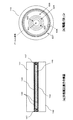
【解決手段】位相補正素子を用いてレーザ光の波面を調整する。位相補正素子は、電極層143と、これに対向して配置された電極層144と、これら電極層143、144の対向面に配された配向膜145と、配向膜145の間に充填された液晶層146とを備える。電極層143には、ビーム入射径の中心から一定距離内にあるレーザ光に球面収差補正作用を付与するための電極E11、E12、E13が配され、それより外側には、区切れのない電極E14が配されている。このように、ビーム入射径よりやや内側に配されていた電極を省略することにより、レンズシフトによる収差の発生を効果的に抑制することができる。
【選択図】図2
Description
本願発明者は、本実施形態に係る図3の位相補正素子を用いた場合と従来例に係る図4の位相補正素子を用いた場合について、ビーム収束位置における波面収差の発生状況の比較検証を行った。以下、これについて説明する。
・対物レンズ焦点距離:2.3mm
・ディスクの基板厚 :0.585mm(基準厚に対する誤差=0.015mm)
・使用レーザの波長 :407nm
14 液晶補正素子
17 対物レンズ
143 電極層
144 電極層
145 配向膜
146 液晶層
E11〜E14 電極(球面収差補正用)
E31〜E38 電極(非点収差補正用)
Claims (6)
- レーザ光源と、
前記レーザ光源から出射されたレーザ光を記録媒体上に収束させる対物レンズと、
前記レーザ光源と前記対物レンズの間に介挿され、且つ、前記対物レンズの有効径内に含まれる前記レーザ光のうち一部にのみ球面収差補正作用を付与する位相補正素子とを有する、
ことを特徴とする光ピックアップ装置。 - 請求項1において、
前記位相補正素子は、前記有効径の中心から一定距離の範囲内にある前記レーザ光に前記球面収差補正作用を付与する、
ことを特徴とする光ピックアップ装置。 - 請求項2において、
前記位相補正素子は、
第1の電極と、
該第1の電極に対向配置された第2の電極と、
前記第1の電極の前記第2の電極に対向する面に配された第1の配向膜と、
前記第2の電極の前記第1の電極に対向する面に配された第2の配向膜と、
前記第1の配向膜と前記第2の配向膜の間に充填された液晶層とを備え、
前記第1の電極は、前記有効径の中心から一定距離内にある前記レーザ光に前記球面収差補正作用を付与するための電極パターンを有する、
ことを特徴とする光ピックアップ装置。 - 請求項2において、
前記位相補正素子は、前記有効径の中心から一定距離の範囲よりも外側において前記レーザ光に前記球面収差の補正作用以外の光学作用を導入する、
ことを特徴とする光ピックアップ装置。 - 請求項4において、
前記位相補正素子は、
第1の電極と、
該第1の電極に対向配置された第2の電極と、
前記第1の電極の前記第2の電極に対向する面に配された第1の配向膜と、
前記第2の電極の前記第1の電極に対向する面に配された第2の配向膜と、
前記第1の配向膜と前記第2の配向膜の間に充填された液晶層とを備え、
前記第1の電極は、前記有効径の中心から一定距離内にある前記レーザ光に前記球面収差補正作用を付与し、前記有効径の中心から一定距離の範囲よりも外側において前記レーザ光に前記球面収差の補正作用以外の光学作用を付与するための電極パターンを有する、
ことを特徴とする光ピックアップ装置。 - 請求項4または5において、
前記位相補正素子は、前記有効径の中心から一定距離の範囲よりも外側において前記レーザ光に非点収差補正作用を付与する、
ことを特徴とする光ピックアップ装置。
Priority Applications (2)
| Application Number | Priority Date | Filing Date | Title |
|---|---|---|---|
| JP2005341551A JP2007164821A (ja) | 2005-11-18 | 2005-11-28 | 光ピックアップ装置 |
| US11/598,565 US20070115767A1 (en) | 2005-11-18 | 2006-11-14 | Optical pickup device |
Applications Claiming Priority (2)
| Application Number | Priority Date | Filing Date | Title |
|---|---|---|---|
| JP2005334708 | 2005-11-18 | ||
| JP2005341551A JP2007164821A (ja) | 2005-11-18 | 2005-11-28 | 光ピックアップ装置 |
Publications (1)
| Publication Number | Publication Date |
|---|---|
| JP2007164821A true JP2007164821A (ja) | 2007-06-28 |
Family
ID=38053306
Family Applications (1)
| Application Number | Title | Priority Date | Filing Date |
|---|---|---|---|
| JP2005341551A Pending JP2007164821A (ja) | 2005-11-18 | 2005-11-28 | 光ピックアップ装置 |
Country Status (2)
| Country | Link |
|---|---|
| US (1) | US20070115767A1 (ja) |
| JP (1) | JP2007164821A (ja) |
Cited By (6)
| Publication number | Priority date | Publication date | Assignee | Title |
|---|---|---|---|---|
| JP2007273045A (ja) * | 2006-03-31 | 2007-10-18 | Toshiba Corp | 光ヘッド及び光ディスク装置 |
| JP2009301648A (ja) * | 2008-06-13 | 2009-12-24 | Pioneer Electronic Corp | 収差補正装置及び光ピックアップ |
| US7978585B2 (en) | 2008-07-31 | 2011-07-12 | Kabushiki Kaisha Toshiba | Aberration correcting device, optical head, and optical disc apparatus |
| KR20190069355A (ko) * | 2019-06-03 | 2019-06-19 | 삼성디스플레이 주식회사 | 픽셀 구조체 및 이를 포함하는 표시장치 |
| KR20200032678A (ko) * | 2019-06-03 | 2020-03-26 | 삼성디스플레이 주식회사 | 픽셀 구조체 및 이를 포함하는 표시장치 |
| US11424229B2 (en) | 2016-06-14 | 2022-08-23 | Samsung Display Co., Ltd. | Pixel structure, display device including the pixel structure, and method of manufacturing the pixel structure |
Family Cites Families (3)
| Publication number | Priority date | Publication date | Assignee | Title |
|---|---|---|---|---|
| JP4180564B2 (ja) * | 2001-08-24 | 2008-11-12 | シャープ株式会社 | 光ピックアップ装置 |
| US7209426B2 (en) * | 2002-11-08 | 2007-04-24 | Citizen Watch Co., Ltd. | Liquid crystal optical element and optical device |
| JP4215011B2 (ja) * | 2004-09-27 | 2009-01-28 | ソニー株式会社 | 光ピックアップ及びこれを用いた光ディスク装置 |
-
2005
- 2005-11-28 JP JP2005341551A patent/JP2007164821A/ja active Pending
-
2006
- 2006-11-14 US US11/598,565 patent/US20070115767A1/en not_active Abandoned
Cited By (10)
| Publication number | Priority date | Publication date | Assignee | Title |
|---|---|---|---|---|
| JP2007273045A (ja) * | 2006-03-31 | 2007-10-18 | Toshiba Corp | 光ヘッド及び光ディスク装置 |
| JP2009301648A (ja) * | 2008-06-13 | 2009-12-24 | Pioneer Electronic Corp | 収差補正装置及び光ピックアップ |
| US7978585B2 (en) | 2008-07-31 | 2011-07-12 | Kabushiki Kaisha Toshiba | Aberration correcting device, optical head, and optical disc apparatus |
| US11424229B2 (en) | 2016-06-14 | 2022-08-23 | Samsung Display Co., Ltd. | Pixel structure, display device including the pixel structure, and method of manufacturing the pixel structure |
| US11424230B2 (en) | 2016-06-14 | 2022-08-23 | Samsung Display Co., Ltd. | Pixel structure and display device including the pixel structure |
| US12094863B2 (en) | 2016-06-14 | 2024-09-17 | Samsung Display Co., Ltd. | Pixel structure, display device including the pixel structure, and method of manufacturing the pixel structure |
| KR20190069355A (ko) * | 2019-06-03 | 2019-06-19 | 삼성디스플레이 주식회사 | 픽셀 구조체 및 이를 포함하는 표시장치 |
| KR102091810B1 (ko) * | 2019-06-03 | 2020-03-23 | 삼성디스플레이 주식회사 | 픽셀 구조체 및 이를 포함하는 표시장치 |
| KR20200032678A (ko) * | 2019-06-03 | 2020-03-26 | 삼성디스플레이 주식회사 | 픽셀 구조체 및 이를 포함하는 표시장치 |
| KR102430815B1 (ko) * | 2019-06-03 | 2022-08-10 | 삼성디스플레이 주식회사 | 픽셀 구조체 및 이를 포함하는 표시장치 |
Also Published As
| Publication number | Publication date |
|---|---|
| US20070115767A1 (en) | 2007-05-24 |
Similar Documents
| Publication | Publication Date | Title |
|---|---|---|
| EP1995725B1 (en) | Optical pickup device | |
| CN1685411B (zh) | 液晶光学元件和光学装置 | |
| JP2009037711A (ja) | 液体レンズ、ピックアップ装置、及び収差補正方法等 | |
| JP2007164821A (ja) | 光ピックアップ装置 | |
| CN101133449B (zh) | 液晶光学元件 | |
| JP2005122828A (ja) | 光ピックアップ装置および光学記録媒体再生装置 | |
| JP4345814B2 (ja) | 収差補正装置、収差補正方法、光ピックアップ | |
| JP4180564B2 (ja) | 光ピックアップ装置 | |
| JP2007149200A (ja) | 光ピックアップ装置および位相補正素子 | |
| CN100454412C (zh) | 光拾取装置 | |
| CN101441878A (zh) | 物镜 | |
| JP4443505B2 (ja) | 光ピックアップ装置および光ディスク装置 | |
| JP4533178B2 (ja) | 光ピックアップ及びこれを用いた光情報処理装置 | |
| WO2007099948A1 (ja) | 収差補正素子、収差補正装置および光ピックアップ | |
| JP4459714B2 (ja) | 液晶収差補正装置及び光ヘッド | |
| JP2006024310A (ja) | 収差補正装置、並びに光ピックアップの制御装置、制御方法及び制御プログラム | |
| JP2002148581A (ja) | 収差補正素子及び収差補正装置 | |
| US7724632B2 (en) | Optical pickup device | |
| KR100759320B1 (ko) | 수차를 보정할 수 있는 광학적 판독 장치 | |
| JP4581969B2 (ja) | 液晶デバイスおよび光ピックアップ | |
| JP2006031829A (ja) | 収差補正装置及び光ヘッド装置 | |
| JP2005267756A (ja) | 位相補正素子、それを用いた光ピックアップ装置及び情報記録再生装置 | |
| CN100481223C (zh) | 光拾取器和使用其的光学信息再现装置 | |
| JP4583444B2 (ja) | 収差補正装置、光ピックアップおよび球面収差補正方法 | |
| JP2005202323A (ja) | 液晶光学素子及び光学装置 |
Legal Events
| Date | Code | Title | Description |
|---|---|---|---|
| A977 | Report on retrieval |
Free format text: JAPANESE INTERMEDIATE CODE: A971007 Effective date: 20080611 |
|
| A131 | Notification of reasons for refusal |
Free format text: JAPANESE INTERMEDIATE CODE: A131 Effective date: 20080617 |
|
| A521 | Request for written amendment filed |
Free format text: JAPANESE INTERMEDIATE CODE: A523 Effective date: 20080725 |
|
| A131 | Notification of reasons for refusal |
Free format text: JAPANESE INTERMEDIATE CODE: A131 Effective date: 20081216 |
|
| A02 | Decision of refusal |
Free format text: JAPANESE INTERMEDIATE CODE: A02 Effective date: 20090804 |