JP2007183452A - Translucent liquid crystal display device - Google Patents
Translucent liquid crystal display device Download PDFInfo
- Publication number
- JP2007183452A JP2007183452A JP2006002126A JP2006002126A JP2007183452A JP 2007183452 A JP2007183452 A JP 2007183452A JP 2006002126 A JP2006002126 A JP 2006002126A JP 2006002126 A JP2006002126 A JP 2006002126A JP 2007183452 A JP2007183452 A JP 2007183452A
- Authority
- JP
- Japan
- Prior art keywords
- interlayer film
- ito
- liquid crystal
- layer
- display device
- Prior art date
- Legal status (The legal status is an assumption and is not a legal conclusion. Google has not performed a legal analysis and makes no representation as to the accuracy of the status listed.)
- Pending
Links
Images



Landscapes
- Liquid Crystal (AREA)
Abstract
Description
本発明は、半透過型液晶表示装置に関し、特に有機層間膜ないし窒化珪素からなる絶縁
層とITOからなる透明導電性膜との間の接着強度が強固で剥離し難く、しかも製造工程
において電蝕が発生し難い半透過型液晶表示装置に関する。
The present invention relates to a transflective liquid crystal display device, and in particular, the adhesive strength between an insulating layer made of an organic interlayer film or silicon nitride and a transparent conductive film made of ITO is strong and difficult to peel off. The present invention relates to a transflective liquid crystal display device that is less likely to cause the occurrence of liquid crystal.
まず、従来例の半透過型表示装置としてアクティブマトリクス型の半透過型液晶表示装
置を例にとり、その数画素部分の平面図である図3及び図3のA−A断面図である図4を
参照して簡単に説明する。
First, as an example of a conventional transflective display device, an active matrix transflective liquid crystal display device is taken as an example, and FIG. 3 which is a plan view of several pixel portions and FIG. A brief description will be given with reference.
従来の半透過型液晶表示装置10は、第1の透光性基板11上にマトリクス状に設けら
れた走査線Xn、Xn+1・・・と信号線Ym、Ym+1・・・で囲まれた領域毎に画素電極
12が設けられているとともに、この画素電極12の反射部の下部にはアルミニウム又は
銀等の金属からなる反射板24が形成されている。また、画素電極12は駆動用の薄膜ト
ランジスタ(Thin Film Transistor)TFTからなる画素トランジスタ14に接続されて
いる。
The conventional transflective liquid
TFTは絶縁ゲート型電界効果トランジスタからからなり、そのソース電極Sは信号線
Ym、Ym+1・・・に接続されて画像信号Vsの供給を受け、また、ドレイン電極Dはコ
ンタクトホール17を経て画素電極12に接続されている。更に、TFTのゲート電極G
は走査線Xn、Xn+1・・・に接続されて所定の電圧を有するゲートパルスVgが印加さ
れるようになされている。
The TFT is composed of an insulated gate field effect transistor, and its source electrode S is connected to the signal lines Ym, Ym + 1... To receive the image signal Vs, and the drain electrode D passes through the
Are connected to the scanning lines Xn, Xn + 1... So that a gate pulse Vg having a predetermined voltage is applied.
なお、ここに示した液晶表示装置10においては、図4に示したように、各TFT、走
査線Xn、Xn+1・・・及び信号線Ym、Ym+1・・・を覆うように、第1の透光性基板
11の表示領域全体に窒化硅素層(以下、SiN層という。)からなる絶縁層22を介し
て層間膜19が所定の高さとなるように設けられており、それぞれの画素毎に反射部の層
間膜19上には反射板24を介して画素電極12が設けられているとともに透過部領域に
は層間膜19の表面に直接画素電極12が設けられている。なお、反射部の層間膜19の
表面は反射光を拡散光とするために表面が僅かに凹凸状態となるようになされているが、
この凹凸状態は図示省略した。
In the liquid
This uneven state is not shown.
更に、第2の透光性基板15にはカラーフィルタ層CFを介して共通電極16が設けら
れているとともに、反射部のセルギャップを透過部領域のセルギャップの半分となるよう
にするためのトップコート層23が設けられている。そして、画素電極12と共通電極1
6との間には液晶20が封入されている。
Further, a
The
この画素電極12及び共通電極16は、通常は透明なITO層から形成されている。こ
のITO層は、高温雰囲気でスパッタリング方法によって成膜することで多結晶状態の膜
とすることができ、得られた多結晶ITO層は、透過率が高くかつ低抵抗であるため、透
明電極として優れている。しかしながら、液晶表示装置においては、成膜したITO層を
個別の電極形状にエッチングしてパターニングする必要があるが、透明電極として優れた
上述の多結晶状態のITO層はエッチングレートが低いためエッチングに時間がかかる。
The
一方、アモルファス状態のITO層はエッチングレートが高いため、これを採用するこ
とでエッチング時間を短縮することが可能となるが、アモルファスITO層は、高抵抗か
つ低透過率であり、電極としての特性が劣るという問題がある。
On the other hand, since the amorphous ITO layer has a high etching rate, it is possible to shorten the etching time by adopting this, but the amorphous ITO layer has high resistance and low transmittance, and has characteristics as an electrode. Is inferior.
そこで、下記特許文献1には、ITO層を常温かつ水添加雰囲気で成膜し、成膜後、1
80℃程度以上、1時間程度以上の熱処理を施すことにより、アモルファス状態のITO
層を作製し、この状態で高いエッチングレートにて所望パターンを形成し、その後、18
0℃程度以上(例えば、220℃程度)の温度で1時間程度以上(例えば1時間程度〜3
時間程度)の熱処理を施すことで、ITO層を多結晶化し、かつ膜の抵抗を低下させ、透
過率を高めるITO層の製造方法の発明が開示されている。
ITO in amorphous state by heat treatment for about 80 ° C or more for about 1 hour or more
In this state, a desired pattern is formed at a high etching rate.
About 1 hour or more (eg, about 1 hour to 3 hours) at a temperature of about 0 ° C. or more (eg, about 220 ° C.)
The invention of the manufacturing method of the ITO layer which polycrystallizes an ITO layer, lowers | hangs the resistance of a film | membrane, and raises the transmittance | permeability is disclosed by performing the heat processing (about time).
しかしながら、一般に層間膜19はポリイミド等の絶縁性の有機樹脂膜から作製される
が、この層間膜19上にアモルファスITO層を設ける場合は、層間膜形成時及びアモル
ファスITO層形成時に焼成工程があるため、有機樹脂膜からガスが発生するので、アモ
ルファスITO層との密着性が悪くなる。また、アモルファスITO層の形成時には基板
表面にSiN層からなる絶縁層が露出している部分が存在するが、この部分においてもア
モルファスITO層の付着性が良好でない。そのため、アモルファスITO層をウェット
エッチングする場合、有機層間膜又はSiNからなる絶縁層上のアモルファスITO層が
逆テーパ形状にエッチングされてしまうことが確認された。
However, in general, the
この状態を図5及び図6を用いて説明する。なお、図5はポリイミドからなる層間膜の
表面に設けたアモルファスITO層のエッチング状態を示す断面図であり、図6はSiN
からなる絶縁層の表面に設けたアモルファスITO層のエッチング状態を示す断面図であ
る。
This state will be described with reference to FIGS. 5 is a cross-sectional view showing the etching state of the amorphous ITO layer provided on the surface of the interlayer film made of polyimide, and FIG.
It is sectional drawing which shows the etching state of the amorphous ITO layer provided in the surface of the insulating layer which consists of.
まず、層間膜19の表面に上記特許文献1に開示されている方法と同様の方法でアモル
ファスITO層31を成膜し、このアモルファスITO層31の表面に所定のパターンと
なるようにフォトレジスト膜32を設け、塩酸と硝酸の混合エッチング液によりアモルフ
ァスITO層31の露出面を湿式エッチングすると、図5に示すように、アモルファスI
TO層31には端面が逆テーパ状となっているサイドエッチング部d1が形成される。同
様にして、SiN層22の表面にアモルファスITO層31を成膜した後にフォトレジス
ト膜32を設け、湿式エッチングすると、図6に示すように、アモルファスITO層31
には端面が逆テーパ状となっているサイドエッチング部d2が形成される。
First, an
The
The side etching part d2 whose end surface is reversely tapered is formed.
このようにアモルファスITO層31の端面に逆テーパ状態が形成されると、アモルフ
ァスITO層31の多結晶ITO層化、フォトレジスト膜32の除去、その他の製造段階
を順に経るに従い、製品として出荷される頃には、多結晶ITOからなる透明導電層と有
機層間膜ないしはSiNからなる絶縁膜との間の付着強度の低下及び電蝕(上記特許文献
2参照)という不都合が発生することが知られている。
When the reverse taper state is formed on the end face of the
本願の発明者等は、上記のような付着強度低下及び電蝕という問題点は有機層間膜ない
しはSiNからなる絶縁膜上に設けられたアモルファスITO層の湿式エッチングの際に
生じる端面が順テーパ状にエッチングされれば生じないことから、このような順テーパ状
にエッチングできる条件を得るべく種々実験を重ねた結果、有機層間膜ないしはSiNか
らなる絶縁膜の表面に変性層を形成させると順テーパ状にエッチングできること、及び、
反射板を層間絶縁膜の変性層上に設けると却って反射板の付着強度が弱くなることから、
反射板自体は層間絶縁膜の表面に直接設ければよいことを見出し、本発明を完成するに至
ったのである。
The inventors of the present application stated that the above-mentioned problems of reduced adhesion strength and electrical corrosion are caused by a forward tapered end face generated during wet etching of an amorphous ITO layer provided on an organic interlayer film or an insulating film made of SiN. As a result of various experiments to obtain such a condition that can be etched in a forward taper shape, if a denatured layer is formed on the surface of an insulating film made of an organic interlayer film or SiN, a forward taper is obtained. That can be etched into a shape, and
If the reflector is provided on the modified layer of the interlayer insulating film, the adhesive strength of the reflector is weakened.
It has been found that the reflector itself may be provided directly on the surface of the interlayer insulating film, and the present invention has been completed.
すなわち、本発明は、有機層間膜と反射板との間の付着強度が高い状態を維持しながら
、有機層間膜ないしはSiNからなる絶縁膜とITO層との間の密着性を改善するととも
に電蝕が生じないようにした、端面が順テーパ状のITO層からなる透明導電層を有する
半透過型液晶表示装置を提供することを目的とする。
That is, the present invention improves the adhesion between the organic interlayer film or the insulating film made of SiN and the ITO layer while maintaining the high adhesion strength between the organic interlayer film and the reflector, and galvanic corrosion. It is an object of the present invention to provide a transflective liquid crystal display device having a transparent conductive layer whose end face is made of an ITO layer having a forward taper shape.
上記目的を達成するため、請求項1に係る半透過型液晶表示装置の発明は、それぞれの
画素毎に有機層間膜の表面の一部に直接反射板が設けられているとともに、前記有機層間
膜及び反射板の表面にITO(Indium Tin Oxide)からなる透明導電層が設けられている
半透過型液晶表示装置において、前記有機層間膜とITOからなる透明導電層との間には
前記有機層間膜の変性層が設けられ、前記変性層上のITOからなる透明導電層の端部が
順テーパ状態となっていることを特徴とする。
In order to achieve the above object, the invention of the transflective liquid crystal display device according to
また、請求項2の発明は、請求項1に記載の半透過型液晶表示装置において、前記変性
層は、前記有機層間膜上に前記反射板を形成した後に、前記有機層間膜表面を不活性ガス
によってプラズマ処理することにより形成されたものであることを特徴とする。
The invention according to
また、請求項3の発明は、請求項1に記載の半透過型液晶表示装置において、前記変性
層は、前記反射板を形成した後に、不活性ガスをキャリアガスとしたプラズマCVD法に
より前記有機層間膜上に形成されたものであることを特徴とする。
The invention according to
また、請求項4の発明は、請求項1に記載の半透過型液晶表示装置において、前記IT
Oからなる透明導電層は、アモルファスITOからなる透明導電層を形成した後に所定の
パターンにエッチングされ、その後多結晶ITO化されたものであることを特徴とする。
According to a fourth aspect of the present invention, in the transflective liquid crystal display device according to the first aspect, the IT
The transparent conductive layer made of O is formed by forming a transparent conductive layer made of amorphous ITO, etching it into a predetermined pattern, and then converting it into polycrystalline ITO.
また、請求項5の発明は、請求項1〜4のいずれかに記載の半透過型液晶表示装置にお
いて、前記反射板の下部の前記有機層間膜の表面は凹凸形状を有することを特徴とする。
The invention according to claim 5 is the transflective liquid crystal display device according to any one of
更に、請求項6に係る半透過型液晶表示装置の発明は、それぞれの画素毎に有機層間膜
の表面の一部に直接反射板が設けられているとともに、前記有機層間膜及び反射板の表面
にITOからなる透明導電層が設けられており、更に窒化硅素からなる絶縁層の表面にも
ITOからなる透明導電層が設けられている半透過型液晶表示装置において、前記有機層
間膜及び窒化珪素からなる絶縁層とITOからなる透明導電層との間にはそれぞれ前記有
機層間膜又は窒化珪素の変性層が設けられ、前記変性層上のITOからなる透明導電層の
端部が順テーパ状態となっていることを特徴とする。
Furthermore, in the invention of the transflective liquid crystal display device according to claim 6, a reflection plate is directly provided on a part of the surface of the organic interlayer film for each pixel, and the surfaces of the organic interlayer film and the reflection plate are provided. In the transflective liquid crystal display device in which a transparent conductive layer made of ITO is provided, and a transparent conductive layer made of ITO is also provided on the surface of the insulating layer made of silicon nitride, the organic interlayer film and silicon nitride The organic interlayer film or the silicon nitride modified layer is provided between the insulating layer made of ITO and the transparent conductive layer made of ITO, respectively, and the end of the transparent conductive layer made of ITO on the modified layer is in a forward tapered state. It is characterized by becoming.
また、請求項7に係る発明は、請求項6に記載の半透過型液晶表示装置において、前記
変性層は、前記有機層間膜上に前記反射板を形成した後に、前記有機層間膜及び窒化珪素
からなる絶縁層を不活性ガスによってプラズマ処理することにより形成されたものである
ことを特徴とする。
The invention according to claim 7 is the transflective liquid crystal display device according to claim 6, wherein the denatured layer is formed by forming the reflector on the organic interlayer film, and then forming the organic interlayer film and silicon nitride. The insulating layer is made by plasma treatment with an inert gas.
また、請求項8に係る発明は、請求項6に記載の半透過型液晶表示装置において、前記
変性層は、前記反射板を形成した後に、不活性ガスをキャリアガスとしたプラズマCVD
法により前記有機層間膜及び窒化珪素からなる絶縁層上に形成されたものであることを特
徴とする。
The invention according to claim 8 is the transflective liquid crystal display device according to claim 6, wherein the modified layer is formed by plasma CVD using an inert gas as a carrier gas after the reflector is formed.
It is formed on the organic interlayer film and the insulating layer made of silicon nitride by the method.
また、請求項9に係る発明は、請求項6に記載の半透過型液晶表示装置において、前記
ITOからなる透明導電層は、アモルファスITOからなる透明導電層を形成した後に所
定のパターンにエッチングされ、その後多結晶ITO化されたものであることを特徴とす
る。
The invention according to claim 9 is the transflective liquid crystal display device according to claim 6, wherein the transparent conductive layer made of ITO is etched into a predetermined pattern after the transparent conductive layer made of amorphous ITO is formed. Then, it is characterized by being made into polycrystalline ITO.
また、請求項10に係る発明は、請求項6〜9のいずれかに記載の半透過型液晶表示装
置において、前記反射板の下部の前記有機層間膜の表面は凹凸形状を有することを特徴と
する。
The invention according to
本発明は上記の構成を備えることにより、以下に述べるような優れた効果を奏する。す
なわち、請求項1に係る発明によれば、ITOからなる透明電極は有機層間膜の表面に設
けられた変性層上に設けられているとともに端部が順テーパ状態となっているから、IT
Oからなる透明電極と有機層間膜との間の付着強度が大きく、電蝕が生じない半透過型液
晶表示装置が得られる。加えて、反射板は、有機層間膜の表面に直接設けられているので
、付着強度が低下することがない。なお、請求項1に係る発明における透明導電層は、そ
れぞれの画素毎に設けられる画素電極以外に、透明な導電性配線として設けられている部
分も含む。
By providing the above configuration, the present invention has the following excellent effects. That is, according to the invention according to
A transflective liquid crystal display device having a high adhesion strength between the transparent electrode made of O and the organic interlayer film and free from electric corrosion is obtained. In addition, since the reflection plate is directly provided on the surface of the organic interlayer film, the adhesion strength does not decrease. In addition, the transparent conductive layer in the invention which concerns on
また、請求項2及び3に係る発明によれば、反射板と有機層間膜との間の付着強度が大
きい状態を維持することができるとともに、有機層間膜の表面を変性させること(請求項
2)、ないしは、有機層間膜の表面に変性層を積層することができ(請求項3)るため、
熱的に安定しているとともにITOとの付着強度の強い変性層が得られる。
Moreover, according to the
A modified layer that is thermally stable and has high adhesion strength with ITO is obtained.
また、請求項4の発明によれば、アモルファスITO層は多結晶ITOよりもエッチン
グレートが高いため、エッチング時間を短縮することが可能となり、また、多結晶ITO
層はアモルファスITO層よりも低抵抗でかつ高透過率であるため、製造時間を短縮でき
、しかも、光学特性及び電気特性に優れた半透過型液晶表示装置が得られる。
According to the invention of claim 4, since the amorphous ITO layer has an etching rate higher than that of polycrystalline ITO, the etching time can be shortened.
Since the layer has a lower resistance and higher transmittance than the amorphous ITO layer, the manufacturing time can be shortened, and a transflective liquid crystal display device excellent in optical characteristics and electrical characteristics can be obtained.
また、請求項5の発明によれば、反射板で反射される光が凹凸によって拡散されるため
、反射部の視野角が広く、明るい表示の半透過型液晶表示装置が得られる。
According to the invention of claim 5, since the light reflected by the reflector is diffused by the unevenness, a transflective liquid crystal display device with a wide viewing angle and a bright display can be obtained.
更に、請求項6に係る発明によれば、ITOからなる透明電極は有機層間膜もしくは窒
化珪素からなる絶縁層の表面に設けられた変性層上に設けられているとともに端部が順テ
ーパ状態となっているから、ITOからなる透明電極と有機層間膜又は窒化珪素からなる
絶縁層との間の付着強度が大きく、電蝕が生じない表示装置が得られる。加えて、反射板
は、有機層間膜の表面に直接設けられているので、付着強度が低下することがない。なお
、請求項6に係る発明における透明導電層は、それぞれの画素毎に設けられる画素電極以
外に、透明な導電性配線として設けられている部分も含む。
Further, according to the invention of claim 6, the transparent electrode made of ITO is provided on the modified layer provided on the surface of the organic interlayer film or the insulating layer made of silicon nitride, and the end portion is in a forward tapered state. Therefore, a display device having a high adhesion strength between the transparent electrode made of ITO and the insulating layer made of the organic interlayer film or silicon nitride can be obtained. In addition, since the reflection plate is directly provided on the surface of the organic interlayer film, the adhesion strength does not decrease. In addition, the transparent conductive layer in the invention which concerns on Claim 6 contains the part provided as transparent conductive wiring other than the pixel electrode provided for every pixel.
また、請求項7及び8に係る発明によれば、反射板と有機層間膜との間の付着強度が大
きい状態を維持することができるとともに、有機層間膜及び窒化珪素からなる絶縁層の表
面を変性させること(請求項7)、ないしは、有機層間膜及び窒化珪素からなる絶縁層の
表面に変性層を積層することができ(請求項8)るため、熱的に安定しているとともにI
TOとの付着強度の強い変性層が得られる。
Moreover, according to the invention which concerns on Claim 7 and 8, while maintaining the state with the large adhesion strength between a reflecting plate and an organic interlayer film, the surface of the insulating layer which consists of an organic interlayer film and silicon nitride is provided. Since the modification layer can be laminated on the surface of the insulating layer made of the organic interlayer film and silicon nitride (claim 8), it is thermally stable and I
A modified layer having strong adhesion strength with TO is obtained.
また、請求項9の発明によれば、アモルファスITO層は多結晶ITOよりもエッチン
グレートが高いため、エッチング時間を短縮することが可能となるので、また、多結晶I
TO層はアモルファスITO層よりも低抵抗でかつ高透過率であるため、製造時間を短縮
でき、しかも、光学特性及び電気特性に優れた半透過型液晶表示装置が得られる。
According to the invention of claim 9, since the amorphous ITO layer has an etching rate higher than that of polycrystalline ITO, it becomes possible to shorten the etching time.
Since the TO layer has a lower resistance and higher transmittance than the amorphous ITO layer, the manufacturing time can be shortened, and a transflective liquid crystal display device excellent in optical characteristics and electrical characteristics can be obtained.
また、請求項10の発明によれば、反射板で反射される光が凹凸によって拡散されるた
め、反射部の視野角が広く、明るい表示の半透過型の表示装置が得られる。
According to the invention of
以下、本発明に係る半透過型液晶表示装置の実施例を図1及び図2を参照して詳細に説
明する。ただし、以下に示す実施例は、本発明の技術思想を具体化するための有機層間膜
又は窒化珪素からなる絶縁層へのITOからなる透明電極を形成した例を液晶表示装置を
例にとり説明するものであって、本発明をこれに特定することを意図するものではなく、
本発明は特許請求の範囲に示した技術思想を逸脱することなく種々の変更を行ったものに
も均しく適用し得るものである。
Hereinafter, embodiments of a transflective liquid crystal display device according to the present invention will be described in detail with reference to FIGS. However, in the following embodiments, an example in which a transparent electrode made of ITO is formed on an organic interlayer film or an insulating layer made of silicon nitride for embodying the technical idea of the present invention will be described taking a liquid crystal display device as an example. And is not intended to identify the present invention,
The present invention can be equally applied to various changes made without departing from the technical idea shown in the claims.
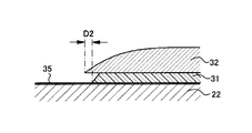
なお、図1は実施例におけるポリイミドからなる層間膜の表面に設けたアモルファスI
TOのエッチング状態を示す断面図であり、図2は実施例におけるSiNからなる絶縁膜
の表面に設けたアモルファスITOのエッチング状態を示す断面図であり、図5及び図6
における構成部分と同一の構成には同じ参照符号を付与して説明する。また、この層間膜
上へのITOからなる透明電極を形成した液晶表示装置の基本的構成及び動作原理は、図
3及び図4に示した従来例の半透過型液晶表示装置50と同様であるので、必要に応じて
図3及び図4を引用して説明することとする。
FIG. 1 shows amorphous I provided on the surface of an interlayer film made of polyimide in the embodiment.
FIG. 2 is a cross-sectional view showing the etching state of TO, and FIG. 2 is a cross-sectional view showing the etching state of amorphous ITO provided on the surface of the insulating film made of SiN in the embodiment.
The same reference numerals are given to the same components as those in FIG. The basic configuration and operation principle of the liquid crystal display device in which the transparent electrode made of ITO is formed on the interlayer film are the same as those of the conventional transflective liquid
本実施例にかかる液晶表示装置10は、以下の工程により製造される。まず、図3及び
図4に示すように、第1の透光性基板11の表面に直接ないしは絶縁膜(図示せず)を介
して、所定パターンに走査線X1、・・・、Xnを形成する。このとき、ゲート電極Gが
走査線X1、・・・、Xnと同時に形成されると共に、補助容量電極13もこの走査線X
1、・・・、Xnと同時に形成される。この走査線X1、・・・、Xn、ゲート電極G及
び補助容量電極13はMo/Al又はアルミニウム合金等の遮光性導電性部材からなる。
The liquid
1 ,..., Xn. The scanning lines X 1 ,..., Xn, the gate electrode G, and the auxiliary capacitance electrode 13 are made of a light-shielding conductive member such as Mo / Al or aluminum alloy.
次にこの第1の透光性基板11表面をSiNからなるゲート絶縁膜18により被覆し、
このゲート絶縁膜18を介してゲート電極Gと対向するようにアモルファス−Si層21
を形成し、次いで、Mo/Al/Moからなる金属層を表示領域全面に設けた後にエッチ
ングすることにより、信号線Y1、・・・、Ymを前記走査線X1、・・・、Xnに直交
する方向に形成するとともに、アモルファス−Si層21上に部分的に重なるように信号
線Y1、・・・、Ymから延設されたソース電極Sと、ドレイン電極Dを設ける。これに
よりTFT構造の画素トランジスタ14が形成される。
Next, the surface of the first translucent substrate 11 is covered with a gate insulating film 18 made of SiN,
The amorphous-
Then, a metal layer made of Mo / Al / Mo is provided on the entire display region and then etched, whereby the signal lines Y 1 ,..., Ym are connected to the scanning lines X 1 ,. The source electrode S and the drain electrode D extending from the signal lines Y 1 ,..., Ym are provided so as to partially overlap the amorphous-
この画素トランジスタ14のドレイン電極Dはゲート絶縁膜18を介して補助容量電極
13に対向配置され、これにより補助容量Csが形成される。その後、各画素トランジス
タ14、走査線Xn、Xn+1・・・及び信号線Ym、Ym+1・・・を覆うようにSiNか
らなる絶縁層22を形成し、次いで第1の透光性基板11の表示領域全体を被覆するよう
に例えばポリイミドからなる層間膜19を所定高さとなるように設け、反射部の層間膜1
9の表面に常法により微細な凹凸を設ける。この微細な凹凸は、この後に設けられる反射
板24の表面が凹凸状になるようにし、反射板24により反射された反射光を拡散させる
ことにより反射部での視野角を広くするとともに反射部の表示が明るくなるようにするた
めのものである。なお、図面においては微小な凹凸は省略されている。
The drain electrode D of the
Fine irregularities are provided on the surface of 9 by a conventional method. This fine unevenness makes the surface of the
その後、層間膜19の表面全体に例えばアルミニウム金属を被覆し、フォトリソグラフ
ィー法により所定パターンにフォトレジストを設けた後、エッチングすることによりそれ
ぞれの画素毎に所定のパターンの反射板24を形成する。そして、露出している層間膜1
9の表面を変性化する。
Thereafter, the entire surface of the
The surface of 9 is modified.
次いで、反射板24及び層間膜19にコンタクトホール17を形成した後、表示領域全
体にわたってアモルファスITOからなる透明導電性材料で被覆する。このとき、アモル
ファスITOからなる画素電極12部分とドレイン電極Dはコンタクトホール17の部分
で電気的に接続される。次いで、フォトリソグラフィー法により所定パターンにフォトレ
ジストを設けた後、塩酸と硝酸の混合エッチング液によりアモルファスITO層の露出面
を湿式エッチングし、それぞれの画素毎に反射板24の表面及び層間膜19の表面にアモ
ルファスITOからなる画素電極12を形成する。その後、熱処理を施して、アモルファ
スITO層を多結晶化し、かつ膜の抵抗を低下させて多結晶ITOからなる画素電極12
を得る。なお、この変性化工程及び画素電極12の具体的な製造工程については後述する
。
Next, after forming contact holes 17 in the
Get. The modification process and the specific manufacturing process of the
そして、別途第2の透光性基板15の表面にカラーフィルタ層CF、ITOからなる透
明な共通電極16、及び反射部に対応する位置にのみトップコート層23を形成したカラ
ーフィルタ基板を第1の透光性基板11と対向させ、この間に液晶20を封入することに
より本実施例の半透過型液晶表示装置10が完成される。なお、トップコート層23は、
反射部のセルギャップが透過部のセルギャップの1/2となるようにするために設けられ
るものである。
Then, the first color filter substrate in which the color filter layer CF, the transparent
It is provided so that the cell gap of the reflection part becomes 1/2 of the cell gap of the transmission part.
ここで、この実施例における層間膜19の表面の変性化工程及び画素電極12の具体的
な製造工程を、図1を参照しながら説明する。なお、図1は実施例におけるポリイミドか
らなる層間膜の表面に設けたアモルファスITOのエッチング状態を示す断面図である。
Here, the modification process of the surface of the
まず、層間膜19及び反射板24を形成した第1の透光性基板11の表面に常法により
Heガスのプラズマ処理を行う。このとき、Heガスのプラズマはポリイミドからなる層
間膜19の表面に接触し、これによりポリイミドの一部が熱分解及びスパッタリングされ
、変性されて変性層34が形成される。
First, a He gas plasma treatment is performed on the surface of the first translucent substrate 11 on which the
その後、上述の特許文献1に開示されている方法と同様にして、変性層34上にアモル
ファスITO層を常温かつ水添加雰囲気でプラズマCVD法により成膜し、成膜後に18
0℃程度以上、1時間程度以上の熱処理を施すことにより、アモルファスITO層31に
変換する。
Thereafter, in the same manner as the method disclosed in
The
次いで、アモルファスITO層31の表面に所定のパターンとなるようにフォトレジス
ト膜32を設け、塩酸と硝酸の混合エッチング液によりアモルファスITO層31の露出
面を湿式エッチングする。そうすると、層間膜19の変性層34上のアモルファスITO
層31は、図1に示したように、端面が順テーパ状となったサイドエッチング部D1が形
成された状態となる。
Next, a
As shown in FIG. 1, the
したがって、この工程後のアモルファスITO層31の多結晶ITO層化、フォトレジ
スト膜32の除去、その他の製造段階を順に経ても、製品として出荷される多結晶ITO
からなる画素電極12を含む透明導電層と有機層間膜19との間の付着強度の低下及び電
蝕が生じることがなくなり、安定な品質の半透過型液晶表示装置が得られる。
Therefore, after the process, the
Thus, the adhesive strength between the transparent conductive layer including the
このような有機層間膜19上に変性層34を設けることによって上述のような作用・効
果が生じることの理由は次のような理由によるものと推測される。すなわち、Heガスの
プラズマは、超高温であるため、ポリイミドからなる層間膜19の表面に接触した際にポ
リイミドの一部を熱分解及びスパッタリングさせるが、同時にポリイミドの表面の一部を
溶融する。この溶融したポリイミドはその後に固まって硬化した変性層34が得られる。
この硬化した変性層34は、表面が熱的に安定しているとともに、以降の高温処理工程で
たとえ層間膜19からガスが発生することがあってもこのガスの透過を抑制し、変性層3
4の表面から上部へのガスの流出が抑えられるため、ITO層と変性層34との間の密着
性が改善されるものと推測される。
The reason why the above-described action and effect are caused by providing the modified
The cured modified
Since the outflow of gas from the surface of 4 to the upper part is suppressed, it is estimated that the adhesion between the ITO layer and the modified
なお、本実施例における半透過型液晶表示装置10においては、一般的にSiNからな
る絶縁層22が露出することはなく、したがってSiNからなる絶縁層22の表面にIT
Oを設けることはない。しかしながら、半透過型液晶表示装置の額縁部での各種接続配線
を複層構造とする場合あるいは検査用端子を設ける場合などにおいては、SiNからなる
絶縁層22の表面にITO層を設ける場合がある。このような場合においても、SiNか
らなる絶縁層22の表面に変性層35を設けることは有効である。
In the transflective liquid
O is not provided. However, when various connection wirings in the frame portion of the transflective liquid crystal display device have a multilayer structure or when an inspection terminal is provided, an ITO layer may be provided on the surface of the insulating
すなわち、図2に示すように、SiNからなる絶縁膜22の表面に上述の場合と同様に
してHeガスのプラズマにより変性層35を形成し、この変性層35上にアモルファスI
TO層を常温かつ水添加雰囲気でプラズマCVD法により成膜し、成膜後に180℃程度
以上、1時間程度以上の熱処理を施すことにより、アモルファスITO層31に変換する
。
That is, as shown in FIG. 2, a modified
The TO layer is formed by a plasma CVD method at room temperature and in a water-added atmosphere, and is converted to the
次いで、アモルファスITO層31の表面に所定のパターンとなるようにフォトレジス
ト膜32を設け、塩酸と硝酸の混合エッチング液によりアモルファスITO層31の露出
面を湿式エッチングする。そうすると、SiNからなる絶縁膜22の変性層35上のアモ
ルファスITO層31は、図2に示したように、端面が順テーパ状となったサイドエッチ
ング部D2が形成された状態となる。
Next, a
したがって、この場合においても、その他の製造段階を順に経ても、製品として出荷さ
れる多結晶ITOとSiNからなる絶縁膜22との間の付着強度の低下及び電蝕が生じる
ことがなくなり、安定な品質の半透過型液晶表示装置が得られる。
Accordingly, even in this case, even if the other manufacturing steps are sequentially performed, the adhesion strength between the polycrystalline ITO shipped as a product and the insulating
10、50 液晶表示装置
11 第1の透光性基板
12 画素電極
13 補助容量電極
14 画素トランジスタ
15 透光性基板
16 共通電極
17 コンタクトホール
18 ゲート絶縁膜
19 層間膜
20 液晶
21 アモルファス−Si層
22 SiNからなる絶縁層
23 トップコート層
24 反射板
31 アモルファスITO層
32 フォトレジスト膜
34、35 変性層
CF カラーフィルタ層
d1、d2 逆テーパ状のサイドエッチング部
D1、D2 順テーパ状のサイドエッチング部
DESCRIPTION OF
Claims (10)
前記有機層間膜及び反射板の表面にITO(Indium Tin Oxide)からなる透明導電層が設
けられている半透過型液晶表示装置において、前記有機層間膜とITOからなる透明導電
層との間には前記有機層間膜の変性層が設けられ、前記変性層上のITOからなる透明導
電層の端部が順テーパ状態となっていることを特徴とする半透過型液晶表示装置。 A direct reflector is provided on a part of the surface of the organic interlayer film for each pixel,
In the transflective liquid crystal display device in which a transparent conductive layer made of ITO (Indium Tin Oxide) is provided on the surface of the organic interlayer film and the reflector, the gap between the organic interlayer film and the transparent conductive layer made of ITO is between A transflective liquid crystal display device, wherein a modified layer of the organic interlayer film is provided, and an end of a transparent conductive layer made of ITO on the modified layer is in a forward tapered state.
不活性ガスによってプラズマ処理することにより形成されたものであることを特徴とする
請求項1に記載の半透過型液晶表示装置。 The said denatured layer is formed by plasma-treating the surface of the organic interlayer film with an inert gas after forming the reflector on the organic interlayer film. Transflective liquid crystal display device.
CVD法により前記有機層間膜上に形成されたものであることを特徴とする請求項1に記
載の半透過型液晶表示装置。 2. The transflective layer according to claim 1, wherein the denatured layer is formed on the organic interlayer film by a plasma CVD method using an inert gas as a carrier gas after the reflection plate is formed. Type liquid crystal display device.
後に所定のパターンにエッチングされ、その後多結晶ITO化されたものであることを特
徴とする請求項1に記載の半透過型液晶表示装置。 The translucent layer according to claim 1, wherein the transparent conductive layer made of ITO is formed into a polycrystalline ITO after being etched into a predetermined pattern after forming the transparent conductive layer made of amorphous ITO. Type liquid crystal display device.
1〜4のいずれかに記載の半透過型液晶表示装置。 The transflective liquid crystal display device according to claim 1, wherein a surface of the organic interlayer film under the reflector has an uneven shape.
前記有機層間膜及び反射板の表面にITOからなる透明導電層が設けられており、更に窒
化硅素からなる絶縁層の表面にもITOからなる透明導電層が設けられている半透過型液
晶表示装置において、前記有機層間膜及び窒化珪素からなる絶縁層とITOからなる透明
導電層との間にはそれぞれ前記有機層間膜又は窒化珪素の変性層が設けられ、前記変性層
上のITOからなる透明導電層の端部が順テーパ状態となっていることを特徴とする半透
過型液晶表示装置。 A direct reflector is provided on a part of the surface of the organic interlayer film for each pixel,
A transflective liquid crystal display device in which a transparent conductive layer made of ITO is provided on the surfaces of the organic interlayer film and the reflector, and a transparent conductive layer made of ITO is also provided on the surface of an insulating layer made of silicon nitride. The organic interlayer film and the insulating layer made of silicon nitride and the transparent conductive layer made of ITO are provided with a modified layer of the organic interlayer film or silicon nitride, respectively, and the transparent conductive film made of ITO on the modified layer A transflective liquid crystal display device characterized in that the end of the layer is in a forward tapered state.
化珪素からなる絶縁層を不活性ガスによってプラズマ処理することにより形成されたもの
であることを特徴とする請求項6に記載の半透過型液晶表示装置。 The denatured layer is formed by plasma-treating the insulating layer made of the organic interlayer film and silicon nitride with an inert gas after forming the reflector on the organic interlayer film. The transflective liquid crystal display device according to claim 6.
CVD法により前記有機層間膜及び窒化珪素からなる絶縁層上に形成されたものであるこ
とを特徴とする請求項6に記載の半透過型液晶表示装置。 The modified layer is formed on the insulating layer made of the organic interlayer film and silicon nitride by plasma CVD using an inert gas as a carrier gas after the reflection plate is formed. Item 7. A transflective liquid crystal display device according to item 6.
後に所定のパターンにエッチングされ、その後多結晶ITO化されたものであることを特
徴とする請求項6に記載の半透過型液晶表示装置。 The translucent layer according to claim 6, wherein the transparent conductive layer made of ITO is formed into a polycrystalline ITO after being etched into a predetermined pattern after forming the transparent conductive layer made of amorphous ITO. Type liquid crystal display device.
6〜9のいずれかに記載の半透過型液晶表示装置。 10. The transflective liquid crystal display device according to claim 6, wherein a surface of the organic interlayer film under the reflector has an uneven shape.
Priority Applications (1)
| Application Number | Priority Date | Filing Date | Title |
|---|---|---|---|
| JP2006002126A JP2007183452A (en) | 2006-01-10 | 2006-01-10 | Translucent liquid crystal display device |
Applications Claiming Priority (1)
| Application Number | Priority Date | Filing Date | Title |
|---|---|---|---|
| JP2006002126A JP2007183452A (en) | 2006-01-10 | 2006-01-10 | Translucent liquid crystal display device |
Publications (1)
| Publication Number | Publication Date |
|---|---|
| JP2007183452A true JP2007183452A (en) | 2007-07-19 |
Family
ID=38339609
Family Applications (1)
| Application Number | Title | Priority Date | Filing Date |
|---|---|---|---|
| JP2006002126A Pending JP2007183452A (en) | 2006-01-10 | 2006-01-10 | Translucent liquid crystal display device |
Country Status (1)
| Country | Link |
|---|---|
| JP (1) | JP2007183452A (en) |
Citations (24)
| Publication number | Priority date | Publication date | Assignee | Title |
|---|---|---|---|---|
| JPH09127553A (en) * | 1995-10-31 | 1997-05-16 | Sharp Corp | Transmissive liquid crystal display device and manufacturing method thereof |
| JPH09152625A (en) * | 1995-08-11 | 1997-06-10 | Sharp Corp | Transmissive liquid crystal display device and manufacturing method thereof |
| JPH09236826A (en) * | 1995-09-28 | 1997-09-09 | Sharp Corp | Liquid crystal display device and method of manufacturing the same |
| JPH09293875A (en) * | 1996-04-26 | 1997-11-11 | Canon Inc | Semiconductor element substrate, manufacturing method thereof, and semiconductor device using the substrate |
| JPH10161158A (en) * | 1996-11-29 | 1998-06-19 | Lg Electron Inc | Liquid crystal display device and its production |
| JPH10319226A (en) * | 1997-05-19 | 1998-12-04 | Nippon Sheet Glass Co Ltd | Electrode plate for color display device and color display device |
| JPH11119261A (en) * | 1995-08-11 | 1999-04-30 | Sharp Corp | Liquid crystal display device, active matrix substrate, and method of manufacturing liquid crystal display device |
| JP2000180840A (en) * | 1998-12-17 | 2000-06-30 | Nippon Sheet Glass Co Ltd | Substrate with transparent electrically conductive ito film and its production |
| JP2000347182A (en) * | 1999-06-02 | 2000-12-15 | Seiko Epson Corp | Color filter substrate, and liquid crystal device and electronic device using the same |
| JP2001255543A (en) * | 2000-03-10 | 2001-09-21 | Hitachi Ltd | Liquid crystal display |
| JP2001296559A (en) * | 1995-08-11 | 2001-10-26 | Sharp Corp | Liquid crystal display device and active matrix substrate |
| WO2002056282A1 (en) * | 2001-01-12 | 2002-07-18 | Nippon Sheet Glass Co., Ltd. | Electrode plate for color display unit and production method therefor |
| JP2002352627A (en) * | 2001-05-23 | 2002-12-06 | Matsushita Electric Ind Co Ltd | Indium tin oxide thin film, method for producing the same, and liquid crystal display device |
| JP2003016858A (en) * | 2001-06-29 | 2003-01-17 | Sanyo Electric Co Ltd | Method for producing indium tin oxide film |
| JP2003140191A (en) * | 2001-11-02 | 2003-05-14 | Samsung Electronics Co Ltd | Reflection-transmission type liquid crystal display device and method of manufacturing the same |
| JP2003149433A (en) * | 2001-08-28 | 2003-05-21 | Seiko Epson Corp | Color filter substrate, liquid crystal device using the same, method for manufacturing color filter substrate, and method for manufacturing liquid crystal device |
| JP2003202587A (en) * | 2001-12-28 | 2003-07-18 | Sanyo Electric Co Ltd | Display device and method of manufacturing the same |
| JP2003222894A (en) * | 2002-01-31 | 2003-08-08 | Matsushita Electric Ind Co Ltd | Liquid crystal display device and method of manufacturing the same |
| JP2003255375A (en) * | 2002-03-04 | 2003-09-10 | Sanyo Electric Co Ltd | Liquid crystal display |
| JP2003255378A (en) * | 2002-03-05 | 2003-09-10 | Sanyo Electric Co Ltd | Liquid crystal display |
| JP2003255332A (en) * | 2002-03-01 | 2003-09-10 | Semiconductor Energy Lab Co Ltd | Liquid crystal display |
| JP2003255374A (en) * | 2002-03-01 | 2003-09-10 | Semiconductor Energy Lab Co Ltd | Liquid crystal display |
| JP2004318073A (en) * | 2003-04-15 | 2004-11-11 | Lg Phillips Lcd Co Ltd | Transflective liquid crystal display device and method of manufacturing the same |
| JP2006301243A (en) * | 2005-04-20 | 2006-11-02 | Sanyo Epson Imaging Devices Corp | Display device |
-
2006
- 2006-01-10 JP JP2006002126A patent/JP2007183452A/en active Pending
Patent Citations (24)
| Publication number | Priority date | Publication date | Assignee | Title |
|---|---|---|---|---|
| JPH09152625A (en) * | 1995-08-11 | 1997-06-10 | Sharp Corp | Transmissive liquid crystal display device and manufacturing method thereof |
| JPH11119261A (en) * | 1995-08-11 | 1999-04-30 | Sharp Corp | Liquid crystal display device, active matrix substrate, and method of manufacturing liquid crystal display device |
| JP2001296559A (en) * | 1995-08-11 | 2001-10-26 | Sharp Corp | Liquid crystal display device and active matrix substrate |
| JPH09236826A (en) * | 1995-09-28 | 1997-09-09 | Sharp Corp | Liquid crystal display device and method of manufacturing the same |
| JPH09127553A (en) * | 1995-10-31 | 1997-05-16 | Sharp Corp | Transmissive liquid crystal display device and manufacturing method thereof |
| JPH09293875A (en) * | 1996-04-26 | 1997-11-11 | Canon Inc | Semiconductor element substrate, manufacturing method thereof, and semiconductor device using the substrate |
| JPH10161158A (en) * | 1996-11-29 | 1998-06-19 | Lg Electron Inc | Liquid crystal display device and its production |
| JPH10319226A (en) * | 1997-05-19 | 1998-12-04 | Nippon Sheet Glass Co Ltd | Electrode plate for color display device and color display device |
| JP2000180840A (en) * | 1998-12-17 | 2000-06-30 | Nippon Sheet Glass Co Ltd | Substrate with transparent electrically conductive ito film and its production |
| JP2000347182A (en) * | 1999-06-02 | 2000-12-15 | Seiko Epson Corp | Color filter substrate, and liquid crystal device and electronic device using the same |
| JP2001255543A (en) * | 2000-03-10 | 2001-09-21 | Hitachi Ltd | Liquid crystal display |
| WO2002056282A1 (en) * | 2001-01-12 | 2002-07-18 | Nippon Sheet Glass Co., Ltd. | Electrode plate for color display unit and production method therefor |
| JP2002352627A (en) * | 2001-05-23 | 2002-12-06 | Matsushita Electric Ind Co Ltd | Indium tin oxide thin film, method for producing the same, and liquid crystal display device |
| JP2003016858A (en) * | 2001-06-29 | 2003-01-17 | Sanyo Electric Co Ltd | Method for producing indium tin oxide film |
| JP2003149433A (en) * | 2001-08-28 | 2003-05-21 | Seiko Epson Corp | Color filter substrate, liquid crystal device using the same, method for manufacturing color filter substrate, and method for manufacturing liquid crystal device |
| JP2003140191A (en) * | 2001-11-02 | 2003-05-14 | Samsung Electronics Co Ltd | Reflection-transmission type liquid crystal display device and method of manufacturing the same |
| JP2003202587A (en) * | 2001-12-28 | 2003-07-18 | Sanyo Electric Co Ltd | Display device and method of manufacturing the same |
| JP2003222894A (en) * | 2002-01-31 | 2003-08-08 | Matsushita Electric Ind Co Ltd | Liquid crystal display device and method of manufacturing the same |
| JP2003255332A (en) * | 2002-03-01 | 2003-09-10 | Semiconductor Energy Lab Co Ltd | Liquid crystal display |
| JP2003255374A (en) * | 2002-03-01 | 2003-09-10 | Semiconductor Energy Lab Co Ltd | Liquid crystal display |
| JP2003255375A (en) * | 2002-03-04 | 2003-09-10 | Sanyo Electric Co Ltd | Liquid crystal display |
| JP2003255378A (en) * | 2002-03-05 | 2003-09-10 | Sanyo Electric Co Ltd | Liquid crystal display |
| JP2004318073A (en) * | 2003-04-15 | 2004-11-11 | Lg Phillips Lcd Co Ltd | Transflective liquid crystal display device and method of manufacturing the same |
| JP2006301243A (en) * | 2005-04-20 | 2006-11-02 | Sanyo Epson Imaging Devices Corp | Display device |
Similar Documents
| Publication | Publication Date | Title |
|---|---|---|
| JP3410656B2 (en) | Liquid crystal display device and manufacturing method thereof | |
| JP4472990B2 (en) | Reflective liquid crystal display device and manufacturing method thereof | |
| JP4191641B2 (en) | Transflective liquid crystal display device and manufacturing method thereof | |
| CN1153303C (en) | Display device and method for manufacturing the same | |
| US7833813B2 (en) | Thin film transistor array panel and method of manufacturing the same | |
| US10312266B2 (en) | Display substrate and manufacturing method thereof, and display device | |
| KR100802457B1 (en) | LCD and its manufacturing method | |
| US10211232B2 (en) | Manufacture method of array substrate and array substrate manufactured by the method | |
| US7630049B2 (en) | Display device and method with lower layer film formed on substrate but between transparent conductive film and organic layer and then protective film on the transparent film | |
| JP4354205B2 (en) | Liquid crystal display device and manufacturing method thereof | |
| US8169428B2 (en) | Display substrate, method of manufacturing the same and display device having the same | |
| JP2007183452A (en) | Translucent liquid crystal display device | |
| JP2006301243A (en) | Display device | |
| JP2005352354A (en) | Display device and manufacturing method thereof | |
| TWI390292B (en) | Semi-transflective liquid crystal display panel and manufacturing method thereof | |
| US20210375951A1 (en) | Array substrate, manufacturing method thereof, and display panel | |
| JP2768590B2 (en) | Active matrix substrate | |
| JP4052804B2 (en) | Electrode substrate and method for producing electrode substrate | |
| JP4084630B2 (en) | Liquid crystal display | |
| CN101097362B (en) | Liquid crystal display, forming method thereof and electronic device | |
| JP5032188B2 (en) | Liquid crystal display device and manufacturing method thereof | |
| JP2005275323A (en) | Liquid crystal display device and manufacturing method thereof | |
| JPH11142868A (en) | Liquid crystal display device and its production | |
| JP4814862B2 (en) | Liquid crystal display | |
| TWI331804B (en) | Thin film transistor substrate and manufacturing method thereof and display panel incorporating the same |
Legal Events
| Date | Code | Title | Description |
|---|---|---|---|
| RD04 | Notification of resignation of power of attorney |
Free format text: JAPANESE INTERMEDIATE CODE: A7424 Effective date: 20070404 |
|
| A621 | Written request for application examination |
Free format text: JAPANESE INTERMEDIATE CODE: A621 Effective date: 20080220 |
|
| A711 | Notification of change in applicant |
Free format text: JAPANESE INTERMEDIATE CODE: A711 Effective date: 20100526 |
|
| RD02 | Notification of acceptance of power of attorney |
Free format text: JAPANESE INTERMEDIATE CODE: A7422 Effective date: 20100526 |
|
| A977 | Report on retrieval |
Free format text: JAPANESE INTERMEDIATE CODE: A971007 Effective date: 20101214 |
|
| A131 | Notification of reasons for refusal |
Free format text: JAPANESE INTERMEDIATE CODE: A131 Effective date: 20101221 |
|
| A02 | Decision of refusal |
Free format text: JAPANESE INTERMEDIATE CODE: A02 Effective date: 20110419 |