JP2007194594A - 薄膜トランジスタ - Google Patents
薄膜トランジスタ Download PDFInfo
- Publication number
- JP2007194594A JP2007194594A JP2006314818A JP2006314818A JP2007194594A JP 2007194594 A JP2007194594 A JP 2007194594A JP 2006314818 A JP2006314818 A JP 2006314818A JP 2006314818 A JP2006314818 A JP 2006314818A JP 2007194594 A JP2007194594 A JP 2007194594A
- Authority
- JP
- Japan
- Prior art keywords
- thin film
- oxide semiconductor
- insulating film
- semiconductor thin
- film layer
- Prior art date
- Legal status (The legal status is an assumption and is not a legal conclusion. Google has not performed a legal analysis and makes no representation as to the accuracy of the status listed.)
- Granted
Links
Images


Landscapes
- Thin Film Transistor (AREA)
- Dram (AREA)
Abstract
【解決手段】 基板上にチャネルとして形成される酸化亜鉛を主成分とする酸化物半導体薄膜層と、ゲート絶縁膜と、ゲート電極とを少なくとも有し、該酸化物半導体薄膜層中に水素を少なくとも含有することを特徴とする薄膜トランジスタである。
【選択図】 図5
Description
酸化亜鉛や酸化マグネシウム亜鉛を半導体薄膜層として用いたTFTは、従来液晶ディスプレイに主に用いられているアモルファスシリコン(a−Si:H)を半導体薄膜層として用いたアモルファスシリコンTFTと比較して電子移動度が大きく、優れたTFT特性を有し、また、室温付近の低温でも結晶薄膜が得られることで高い移動度が期待できる等の利点もあり、積極的な開発が進められている。
また、格子欠陥は活性層となる酸化亜鉛中のキャリアの誘起を妨げ、キャリア濃度を減少させる。キャリア濃度の減少は活性層の導電率を引き下げ、薄膜トランジスタの電子移動度、電流伝達特性(例えば、サブスレッショルド特性やしきい電圧)に影響する。
一方、前記格子欠陥以外に酸化亜鉛中に浅い不純物準位を形成する元素として水素が報告されている(例えば、下記非特許文献1参照)。従って、格子欠陥以外にもTFT製造工程で導入される水素等の元素が酸化亜鉛TFTの特性に影響を与えると考えられる。
しかしながら、非特許文献1を含め、酸化亜鉛などの酸化物中の含有元素がTFT特性に与える影響に関する記載がなされた文献は見られない。
また、ゲート絶縁膜が、酸化珪素膜、酸窒化珪素膜、窒化珪素膜、あるいは窒化珪素に酸素もしくは酸素を構成元素に含む化合物を用いることで酸素がドーピングされた膜のいずれかを少なくとも一部に用いた絶縁膜であることにより、ゲート絶縁膜成膜時における酸素又は亜鉛の脱離による格子欠陥を防ぐことができる。そのため、酸化物半導体薄膜層中への水素拡散量をより厳密に制御でき、リーク電流の抑制、しきい電圧の低下、電子移動度の向上といった効果をより確実に奏する薄膜トランジスタとなる。
また、保護絶縁膜が酸化珪素膜、酸窒化珪素膜、窒化珪素膜、あるいは窒化珪素に酸素もしくは酸素を構成元素に含む化合物を用いることで酸素がドーピングされた膜のいずれかを少なくとも一部に用いた絶縁膜であることにより、保護絶縁膜成膜時における酸素又は亜鉛の脱離による格子欠陥を防ぐことができる。そのため、酸化物半導体薄膜層中への水素拡散量をより厳密に制御でき、リーク電流の抑制、しきい電圧の低下、電子移動度の向上といった効果をより確実に奏する薄膜トランジスタとなる。
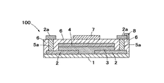
酸化物半導体薄膜層3は、一対のソース・ドレイン電極2の電極間にチャネルを形成するように配置されており、酸化亜鉛を主成分とする酸化物半導体から形成されている。ここで、酸化亜鉛を主成分とする酸化物半導体とは、真性酸化亜鉛の他、Li,Na,N,C等のp型ドーパント及びB,Al,Ga,In等のn型ドーパント、及びMg,Be等がドーピングされた酸化亜鉛を含む。
第一ゲート絶縁膜4及び第二ゲート絶縁膜6は、例えばプラズマ化学気相成長(PCVD)法により形成される。このとき、プラズマ化学気相成長(PCVD)法による成膜は酸化物半導体薄膜層の還元もしくは酸素や亜鉛の脱離が生じない基板温度である250℃以下で実施することが望ましい。
第一ゲート絶縁膜4としては、酸化珪素(SiOx)膜、酸窒化珪素(SiON)膜、窒化珪素(SiNx)膜、あるいは窒化珪素(SiNx)に酸素もしくは酸素を構成元素に含む化合物を用いることで酸素がドーピングされた膜等のシリコン系絶縁膜が用いられることが望ましい。なかでもSiNxに酸素あるいは酸素を構成元素として含む化合物、例えばN2Oを用いて酸素をドーピングした膜などが望ましい。その理由はこれらの構成成分は誘電率が高く、酸化物半導体薄膜層3の亜鉛や酸素の脱離の防止の観点からも優れているからである。
なお、酸化物半導体薄膜層中の水素濃度の制御方法としては、上記したものの他に、ゲート絶縁膜成膜中の基板温度やガス種、プラズマ処理の条件等を変化させる方法も挙げることができる。また、酸化物半導体薄膜層成膜時に水分を導入する、具体的にはスパッタリング中に水蒸気を導入したり、ジエチル亜鉛(DEZ)と水蒸気を交互に導入する原子層製膜(Atomic Layer Deposition:ALD)を行ったりする方法も挙げることができる。
保護絶縁膜13は、酸化珪素(SiOx)膜、酸窒化珪素(SiON)膜、窒化珪素(SiNx)膜、あるいは窒化珪素(SiNx)に酸素もしくは酸素を構成元素に含む化合物を用いることで酸素がドーピングされた膜により形成される。この保護絶縁膜13としては、酸化珪素(SiOx)や酸窒化珪素(SiON)に比較して誘電率の大きい、SiNxに酸素あるいは酸素を構成元素として含む化合物、例えばN2O、を用いることで酸素がドーピングされた膜が好ましく用いられる。
保護絶縁膜13は、例えばプラズマ化学気相成長(PCVD)法により形成される。このとき、プラズマ化学気相成長(PCVD)法による成膜は酸化物半導体薄膜層の還元もしくは亜鉛や酸素の脱離が生じない基板温度である250℃以下で実施することが望ましい。
第一オーバーコート絶縁膜14を設けることで、保護絶縁膜13が被覆していない酸化物半導体薄膜層12の側表面を確実に被覆することができる。
第二オーバーコート絶縁膜16を設けることにより、薄膜トランジスタ101のデバイス全体をより確実に保護することができる。
このゲート絶縁膜11の形成方法は、特に限定されないが、大面積基板への成膜が可能なプラズマ化学気相成長(PCVD)法を用いることが好ましい。
ゲート絶縁膜11の成膜後に、酸素(O2)あるいは亜酸化窒素(N2O)といった酸化性ガスを用いたプラズマにより、基板表面を清浄化することが好ましい。特に、酸化性ガスとして酸素を用いた場合は、ArやXe、He、Krといった希ガスを酸素に添加したプラズマを用いることで、酸素ラジカルの発生量が増大し、酸化物半導体薄膜層表面に吸着された有機成分や水分に対するクリーニング効率が増大すると同時に、添加ガスによるスパッタ効果により酸化物半導体薄膜層表面の金属不純物が除去可能となるため、より好ましい。
保護絶縁膜13は、酸化珪素(SiOx)膜、酸窒化珪素(SiON)膜、窒化珪素(SiNx)膜、あるいは窒化珪素(SiNx)に酸素もしくは酸素を構成元素に含む化合物を用いることで酸素がドーピングされた膜等のシリコン系絶縁膜が用いられることが望ましい。なかでもSiNxに酸素あるいは酸素を構成元素として含む化合物、例えばN2Oを用いることで酸素がドーピングされた膜などが望ましい。その理由はこれらの構成成分は誘電率が高く、酸化物半導体薄膜層3の亜鉛や酸素の脱離の防止の観点からも優れているからである。
保護絶縁膜13の形成に際しては、プラズマ化学気相成長(PCVD)法を用いることが好ましい。
コンタクトホールは、第一オーバーコート絶縁膜14上にコーティングされたフォトレジストに開口部を形成し、この開口部を介してエッチングすることにより、保護絶縁膜13及び第一オーバーコート絶縁膜14を貫通して酸化物半導体薄膜層12の表面に達する深さに形成する。
一対のソース・ドレイン電極15はコンタクトホールをそれぞれ充填して、間隔を有して形成される。
以下、本発明に係る薄膜トランジスタの試験例を比較することにより、本発明の効果をより明確なものとする。
SiO2とAl2O3を主成分とする無アルカリガラスからなる基板1上にインジウムスズ酸化物(ITO)からなる一対のソース・ドレイン電極2を40nmの厚さで形成した。
基板1及び一対のソース・ドレイン電極2上の全面に酸化物半導体薄膜層3として真性酸化亜鉛をマグネトロンスパッタ法により、50nmの厚さで形成した。
酸化物半導体薄膜層3の形成後、酸化物半導体薄膜層3の上面全面にSiNxからなる第一ゲート絶縁膜4を50nmの厚さで形成した。この第一ゲート絶縁膜の形成は、250℃の条件下で、SiH4+NH3+N2ガスを用いたプラズマ化学気相成長(PCVD)法により行った。
NH3と SiH4の混合ガスを用いて第一ゲート絶縁膜を形成する際、酸化亜鉛活性層中の水素濃度を変化させる目的で、NH3/SiH4ガス流量比を1から20まで変化させた。NH3/SiH4ガス流量比を大きくする事で、ゲート絶縁膜成膜中に酸化物半導体薄膜層に取り込まれる水素濃度が増大する。
次に、第一ゲート絶縁膜4上にフォトレジストをコーティングし、パターニングされたフォトレジスト4aをマスクとして、第一ゲート絶縁膜4をCF4+O2のガスを用いてドライエッチングした。
第一ゲート絶縁膜4のエッチングを行った後、0.2%HNO3溶液を用いて酸化物半導体薄膜層に対しウェットエッチングを行い、フォトレジストを除去し、基板1、一対のソース・ドレイン電極2、酸化物半導体薄膜層3、及び第一ゲート絶縁膜4上全面に亘ってSiNxからなる第二ゲート絶縁膜6を300nm厚で形成した。
この第二ゲート絶縁膜6の形成は、SiH4+NH3+N2ガスを用いたプラズマ化学気相成長(PCVD)法を用い、250℃にて行った。第二ゲート絶縁膜成膜時のNH3/SiH4比は、第一ゲート絶縁膜と同一になるよう設定した。
第二ゲート絶縁膜6の形成後、一対のソース・ドレイン電極2の上部に、フォトリソグラフィー及びCF4+O2のガスを用いてドライエッチングによりコンタクトホール5を開口した。
最後に、Crからなるゲート電極7を第二ゲート絶縁膜6上に100nm厚で形成し、同一材料にて、一対のソース・ドレイン外部電極2aをコンタクト部5aを介してそれぞれ対応するソース・ドレイン電極2と接続するように形成し、インジウムスズ酸化物(ITO)からなる表示電極8を第二ゲート絶縁膜6の一部上に100nm厚で形成して薄膜トランジスタを作成した。
今回はガス流量比を変化させて酸化物半導体薄膜層中への水素濃度制御を実施したが、特に本手法に限る必要はなく、ゲート絶縁膜成膜中の基板温度やガス種、プラズマ処理の条件等を変化させても同様に酸化物半導体薄膜層の水素濃度を制御可能である。或いは酸化物半導体薄膜層成膜時に水分を導入する、具体的にはスパッタリング中に水蒸気を導入したり、ジエチル亜鉛(DEZ)と水蒸気を交互に導入する原子層製膜(Atomic Layer Deposition:ALD)等の手法によっても酸化亜鉛中の水素濃度を制御できる。
作成したそれぞれの薄膜トランジスタの酸化物半導体活性層中に含まれる水素濃度を二次イオン質量分析(SIMS)装置にて測定し、薄膜トランジスタの伝達特性の評価を行った。
その結果を図5に示す。
以上の結果より、液晶ディスプレイの駆動素子として用いる薄膜トランジスタはリーク電流が小さい事が要求されるため、活性層中の水素濃度を5×1020cm−3以上、7×1021cm−3以下とすることで低リーク電流を維持した状態で良好なトランジスタ特性が得られる事が明らかとなった。
2 ソース・ドレイン電極
3 酸化物半導体薄膜層
4 第一ゲート絶縁膜
6 第二ゲート絶縁膜
7 ゲート電極
9 基板
10 ゲート電極
11 ゲート絶縁膜
12 酸化物半導体薄膜層
13 保護絶縁膜
14 第一オーバーコート絶縁膜
15 ソース・ドレイン電極
16 第二オーバーコート絶縁膜
100 トップゲート型薄膜トランジスタ
101 ボトムゲート型薄膜トランジスタ
Claims (4)
- 基板上にチャネルとして形成される酸化亜鉛を主成分とする酸化物半導体薄膜層と、ゲート絶縁膜と、ゲート電極とを少なくとも有し、該酸化物半導体薄膜層中に水素を少なくとも含有することを特徴とする薄膜トランジスタ。
- 前記酸化物半導体薄膜層中に含まれる水素濃度が、5×1020cm−3以上、7×1021cm−3以下であることを特徴とする請求項1記載の薄膜トランジスタ。
- 前記薄膜トランジスタが、前記基板上に形成される前記酸化物半導体薄膜層と、該酸化物半導体薄膜層の上表面及び側面を被覆して形成される前記ゲート絶縁膜と、該ゲート絶縁膜上に積載された前記ゲート電極とを有するトップゲート型薄膜トランジスタであって、該ゲート絶縁膜が、酸化珪素膜、酸窒化珪素膜、窒化珪素膜、あるいは窒化珪素に酸素もしくは酸素を構成元素に含む化合物を用いることで酸素がドーピングされた膜のいずれかを少なくとも一部に用いた絶縁膜であることを特徴とする請求項1又は2記載の薄膜トランジスタ。
- 前記薄膜トランジスタが、前記基板上に形成される前記ゲート電極と、該ゲート電極を被覆して形成される前記ゲート絶縁膜と、該ゲート絶縁膜上に形成される前記酸化物半導体薄膜層と、該酸化物半導体薄膜層上に形成される保護絶縁膜とを有するボトムゲート型薄膜トランジスタであって、該保護絶縁膜が酸化珪素膜、酸窒化珪素膜、窒化珪素膜、あるいは窒化珪素に酸素もしくは酸素を構成元素に含む化合物を用いることで酸素がドーピングされた膜のいずれかを少なくとも一部に用いた絶縁膜であることを特徴とする請求項1又は2記載の薄膜トランジスタ。
Priority Applications (1)
| Application Number | Priority Date | Filing Date | Title |
|---|---|---|---|
| JP2006314818A JP5099740B2 (ja) | 2005-12-19 | 2006-11-21 | 薄膜トランジスタ |
Applications Claiming Priority (3)
| Application Number | Priority Date | Filing Date | Title |
|---|---|---|---|
| JP2005364786 | 2005-12-19 | ||
| JP2005364786 | 2005-12-19 | ||
| JP2006314818A JP5099740B2 (ja) | 2005-12-19 | 2006-11-21 | 薄膜トランジスタ |
Publications (2)
| Publication Number | Publication Date |
|---|---|
| JP2007194594A true JP2007194594A (ja) | 2007-08-02 |
| JP5099740B2 JP5099740B2 (ja) | 2012-12-19 |
Family
ID=38450004
Family Applications (1)
| Application Number | Title | Priority Date | Filing Date |
|---|---|---|---|
| JP2006314818A Expired - Fee Related JP5099740B2 (ja) | 2005-12-19 | 2006-11-21 | 薄膜トランジスタ |
Country Status (1)
| Country | Link |
|---|---|
| JP (1) | JP5099740B2 (ja) |
Cited By (68)
| Publication number | Priority date | Publication date | Assignee | Title |
|---|---|---|---|---|
| EP2159844A2 (en) | 2008-08-28 | 2010-03-03 | Canon Kabushiki Kaisha | Amorphous oxide semiconductor and thin film transistor using the same |
| KR20100103414A (ko) * | 2009-03-13 | 2010-09-27 | 가부시키가이샤 한도오따이 에네루기 켄큐쇼 | 반도체 장치 및 그 제작 방법 |
| JP2011009719A (ja) * | 2009-05-29 | 2011-01-13 | Semiconductor Energy Lab Co Ltd | 半導体装置及びその作製方法 |
| JP2011049549A (ja) * | 2009-07-31 | 2011-03-10 | Semiconductor Energy Lab Co Ltd | 半導体装置及び半導体装置の作製方法 |
| WO2011037010A1 (en) * | 2009-09-24 | 2011-03-31 | Semiconductor Energy Laboratory Co., Ltd. | Semiconductor element and method for manufacturing the same |
| US20110073856A1 (en) * | 2009-09-30 | 2011-03-31 | Canon Kabushiki Kaisha | Thin film transistor |
| JP2011103453A (ja) * | 2009-10-16 | 2011-05-26 | Semiconductor Energy Lab Co Ltd | 論理回路及び半導体装置 |
| WO2011065230A1 (en) * | 2009-11-30 | 2011-06-03 | Semiconductor Energy Laboratory Co., Ltd. | Liquid crystal display device, method for driving the same, and electronic device including the same |
| WO2011070892A1 (en) * | 2009-12-08 | 2011-06-16 | Semiconductor Energy Laboratory Co., Ltd. | Semiconductor device and manufacturing method thereof |
| JP2011120222A (ja) * | 2009-10-30 | 2011-06-16 | Semiconductor Energy Lab Co Ltd | 論理回路及び半導体装置 |
| JP2011119691A (ja) * | 2009-10-30 | 2011-06-16 | Semiconductor Energy Lab Co Ltd | 電界効果型トランジスタ |
| CN102214698A (zh) * | 2010-04-09 | 2011-10-12 | 索尼公司 | 薄膜晶体管、显示装置以及电子单元 |
| JP2011527121A (ja) * | 2008-07-02 | 2011-10-20 | アプライド マテリアルズ インコーポレイテッド | 金属酸窒化物tft用キャッピング層 |
| WO2011112295A3 (en) * | 2010-03-12 | 2011-11-10 | Wisconsin Alumni Research Foundation | Large-area, free-standing metal oxide films and transistors made therefrom |
| WO2011145635A1 (en) * | 2010-05-20 | 2011-11-24 | Semiconductor Energy Laboratory Co., Ltd. | Semiconductor device and manufacturing method of the same |
| JP2011246787A (ja) * | 2010-05-28 | 2011-12-08 | Fujifilm Corp | 導電性酸化亜鉛膜および導電性酸化亜鉛膜を備えた光電変換素子 |
| JP2012075092A (ja) * | 2010-09-03 | 2012-04-12 | Semiconductor Energy Lab Co Ltd | 発振回路およびそれを用いた半導体装置 |
| US8232551B2 (en) | 2008-07-14 | 2012-07-31 | Samsung Electronics Co., Ltd. | Channel layers and semiconductor devices including the same |
| JP2012186797A (ja) * | 2011-02-17 | 2012-09-27 | Semiconductor Energy Lab Co Ltd | プログラマブルlsi |
| JP2012231455A (ja) * | 2011-04-13 | 2012-11-22 | Semiconductor Energy Lab Co Ltd | プログラマブルlsi |
| JP2012248860A (ja) * | 2010-04-23 | 2012-12-13 | Semiconductor Energy Lab Co Ltd | 半導体装置の作製方法 |
| JP2012257188A (ja) * | 2010-08-25 | 2012-12-27 | Semiconductor Energy Lab Co Ltd | ラッチ回路及び半導体装置 |
| JP2012256034A (ja) * | 2011-05-13 | 2012-12-27 | Semiconductor Energy Lab Co Ltd | El表示装置および電子機器 |
| JP2012257197A (ja) * | 2011-03-11 | 2012-12-27 | Semiconductor Energy Lab Co Ltd | 記憶回路 |
| JP2012256033A (ja) * | 2011-05-13 | 2012-12-27 | Semiconductor Energy Lab Co Ltd | 表示装置及び電子機器 |
| JP2013042150A (ja) * | 2009-03-12 | 2013-02-28 | Semiconductor Energy Lab Co Ltd | 半導体装置 |
| JP2013042143A (ja) * | 2008-12-24 | 2013-02-28 | Semiconductor Energy Lab Co Ltd | 半導体装置 |
| US8389991B2 (en) | 2009-12-01 | 2013-03-05 | Sony Corporation | Thin film transistor, display device, and electronic device |
| KR101270174B1 (ko) | 2007-12-03 | 2013-05-31 | 삼성전자주식회사 | 산화물 반도체 박막 트랜지스터의 제조방법 |
| US8502217B2 (en) | 2007-12-04 | 2013-08-06 | Canon Kabushiki Kaisha | Oxide semiconductor device including insulating layer and display apparatus using the same |
| US8513661B2 (en) | 2008-01-23 | 2013-08-20 | Canon Kabushiki Kaisha | Thin film transistor having specified transmittance to light |
| JP2013219336A (ja) * | 2012-03-14 | 2013-10-24 | Semiconductor Energy Lab Co Ltd | 半導体装置の作製方法 |
| JP2014090186A (ja) * | 2013-12-04 | 2014-05-15 | Semiconductor Energy Lab Co Ltd | 半導体装置の作製方法 |
| US8748223B2 (en) | 2009-09-24 | 2014-06-10 | Semiconductor Energy Laboratory Co., Ltd. | Method for manufacturing oxide semiconductor film and method for manufacturing semiconductor device |
| US8759829B2 (en) | 2009-03-27 | 2014-06-24 | Semiconductor Energy Laboratory Co., Ltd. | Semiconductor device comprising oxide semiconductor layer as channel formation layer |
| JP2014123966A (ja) * | 2009-11-20 | 2014-07-03 | Semiconductor Energy Lab Co Ltd | 半導体装置 |
| US8906738B2 (en) | 2010-11-05 | 2014-12-09 | Sony Corporation | Oxide semiconductor thin film transistor with an aluminum oxide protective film made using a continuous deposition process of aluminum oxide laminated with an aluminum film |
| JP2015005672A (ja) * | 2013-06-21 | 2015-01-08 | 出光興産株式会社 | 酸化物トランジスタ |
| US8945982B2 (en) | 2010-04-23 | 2015-02-03 | Semiconductor Energy Laboratory Co., Ltd. | Manufacturing method of semiconductor device |
| JP2015046616A (ja) * | 2009-11-20 | 2015-03-12 | 株式会社半導体エネルギー研究所 | 半導体装置 |
| US8981374B2 (en) | 2013-01-30 | 2015-03-17 | Semiconductor Energy Laboratory Co., Ltd. | Semiconductor device |
| JP2015109083A (ja) * | 2009-11-06 | 2015-06-11 | 株式会社半導体エネルギー研究所 | 半導体装置 |
| JP2016001745A (ja) * | 2008-10-31 | 2016-01-07 | 株式会社半導体エネルギー研究所 | 駆動回路 |
| JP2016006888A (ja) * | 2009-12-11 | 2016-01-14 | 株式会社半導体エネルギー研究所 | 半導体装置 |
| JP2016014882A (ja) * | 2009-10-21 | 2016-01-28 | 株式会社半導体エネルギー研究所 | 液晶表示装置 |
| US9385114B2 (en) | 2009-10-30 | 2016-07-05 | Semiconductor Energy Laboratory Co., Ltd. | Non-linear element, display device including non-linear element, and electronic device including display device |
| JP2016136276A (ja) * | 2010-04-28 | 2016-07-28 | 株式会社半導体エネルギー研究所 | 表示装置及び電子機器 |
| US9494830B2 (en) | 2013-06-05 | 2016-11-15 | Semiconductor Energy Laboratory Co., Ltd. | Sequential circuit and semiconductor device |
| JP2016197739A (ja) * | 2009-09-04 | 2016-11-24 | 株式会社半導体エネルギー研究所 | 半導体装置 |
| US9508276B2 (en) | 2012-06-29 | 2016-11-29 | Semiconductor Energy Laboratory Co., Ltd. | Method of driving display device including comparator circuit, and display device including comparator circuit |
| US9515656B2 (en) | 2013-11-01 | 2016-12-06 | Semiconductor Energy Laboratory Co., Ltd. | Reconfigurable circuit, storage device, and electronic device including storage device |
| JP2016208050A (ja) * | 2009-07-03 | 2016-12-08 | 株式会社半導体エネルギー研究所 | 半導体装置の作製方法 |
| JP2016220251A (ja) * | 2011-05-16 | 2016-12-22 | 株式会社半導体エネルギー研究所 | プログラマブルロジックデバイス |
| JP2017017743A (ja) * | 2011-05-19 | 2017-01-19 | 株式会社半導体エネルギー研究所 | プログラマブルロジックデバイス |
| US9627198B2 (en) | 2009-10-05 | 2017-04-18 | Semiconductor Energy Laboratory Co., Ltd. | Method for manufacturing thin film semiconductor device |
| JP2017107233A (ja) * | 2010-04-23 | 2017-06-15 | 株式会社半導体エネルギー研究所 | 液晶表示装置及びその作製方法 |
| US9698273B2 (en) | 2012-03-30 | 2017-07-04 | Joled Inc. | Thin film transistor, method of manufacturing the same, display unit, and electronic apparatus |
| US9786689B2 (en) | 2009-07-31 | 2017-10-10 | Semiconductor Energy Laboratory Co., Ltd. | Display device |
| JP2017194688A (ja) * | 2010-07-02 | 2017-10-26 | 株式会社半導体エネルギー研究所 | 液晶表示装置 |
| JP2018018102A (ja) * | 2010-02-26 | 2018-02-01 | 株式会社半導体エネルギー研究所 | 液晶表示装置 |
| CN108269854A (zh) * | 2016-12-30 | 2018-07-10 | 乐金显示有限公司 | 薄膜晶体管基板及其制造方法和显示装置 |
| TWI629870B (zh) * | 2009-12-18 | 2018-07-11 | 半導體能源研究所股份有限公司 | 非依電性閂鎖電路及邏輯電路,及使用非依電性閂鎖電路之半導體裝置 |
| US10079306B2 (en) | 2009-07-31 | 2018-09-18 | Semiconductor Energy Laboratory Co., Ltd. | Semiconductor device |
| JP2018160679A (ja) * | 2008-12-05 | 2018-10-11 | 株式会社半導体エネルギー研究所 | 半導体装置の作製方法 |
| JP2019071434A (ja) * | 2010-01-24 | 2019-05-09 | 株式会社半導体エネルギー研究所 | 表示装置 |
| JP2019216285A (ja) * | 2010-01-22 | 2019-12-19 | 株式会社半導体エネルギー研究所 | 半導体装置 |
| US10566459B2 (en) | 2009-10-30 | 2020-02-18 | Semiconductor Energy Laboratory Co., Ltd. | Semiconductor device having a first region comprising silicon, oxygen and at least one metal element formed between an oxide semiconductor layer and an insulating layer |
| JP2023139159A (ja) * | 2010-02-05 | 2023-10-03 | 株式会社半導体エネルギー研究所 | 半導体装置 |
Citations (5)
| Publication number | Priority date | Publication date | Assignee | Title |
|---|---|---|---|---|
| JPH08264794A (ja) * | 1995-03-27 | 1996-10-11 | Res Dev Corp Of Japan | 亜酸化銅等の金属酸化物半導体による薄膜トランジスタとpn接合を形成した金属酸化物半導体装置およびそれらの製造方法 |
| JP2003179233A (ja) * | 2001-12-13 | 2003-06-27 | Fuji Xerox Co Ltd | 薄膜トランジスタ、及びそれを備えた表示素子 |
| JP2004311783A (ja) * | 2003-04-08 | 2004-11-04 | Fuji Xerox Co Ltd | 光検出装置、及びその実装方法 |
| JP2005033172A (ja) * | 2003-06-20 | 2005-02-03 | Sharp Corp | 半導体装置およびその製造方法ならびに電子デバイス |
| JP2007103918A (ja) * | 2005-09-06 | 2007-04-19 | Canon Inc | アモルファス酸化物膜をチャネル層に用いた電界効果型トランジスタ、アモルファス酸化物膜をチャネル層に用いた電界効果型トランジスタの製造方法及びアモルファス酸化物膜の製造方法 |
-
2006
- 2006-11-21 JP JP2006314818A patent/JP5099740B2/ja not_active Expired - Fee Related
Patent Citations (5)
| Publication number | Priority date | Publication date | Assignee | Title |
|---|---|---|---|---|
| JPH08264794A (ja) * | 1995-03-27 | 1996-10-11 | Res Dev Corp Of Japan | 亜酸化銅等の金属酸化物半導体による薄膜トランジスタとpn接合を形成した金属酸化物半導体装置およびそれらの製造方法 |
| JP2003179233A (ja) * | 2001-12-13 | 2003-06-27 | Fuji Xerox Co Ltd | 薄膜トランジスタ、及びそれを備えた表示素子 |
| JP2004311783A (ja) * | 2003-04-08 | 2004-11-04 | Fuji Xerox Co Ltd | 光検出装置、及びその実装方法 |
| JP2005033172A (ja) * | 2003-06-20 | 2005-02-03 | Sharp Corp | 半導体装置およびその製造方法ならびに電子デバイス |
| JP2007103918A (ja) * | 2005-09-06 | 2007-04-19 | Canon Inc | アモルファス酸化物膜をチャネル層に用いた電界効果型トランジスタ、アモルファス酸化物膜をチャネル層に用いた電界効果型トランジスタの製造方法及びアモルファス酸化物膜の製造方法 |
Cited By (220)
| Publication number | Priority date | Publication date | Assignee | Title |
|---|---|---|---|---|
| KR101270174B1 (ko) | 2007-12-03 | 2013-05-31 | 삼성전자주식회사 | 산화물 반도체 박막 트랜지스터의 제조방법 |
| US8502217B2 (en) | 2007-12-04 | 2013-08-06 | Canon Kabushiki Kaisha | Oxide semiconductor device including insulating layer and display apparatus using the same |
| US8513661B2 (en) | 2008-01-23 | 2013-08-20 | Canon Kabushiki Kaisha | Thin film transistor having specified transmittance to light |
| JP2011527121A (ja) * | 2008-07-02 | 2011-10-20 | アプライド マテリアルズ インコーポレイテッド | 金属酸窒化物tft用キャッピング層 |
| US8232551B2 (en) | 2008-07-14 | 2012-07-31 | Samsung Electronics Co., Ltd. | Channel layers and semiconductor devices including the same |
| US8426243B2 (en) | 2008-08-28 | 2013-04-23 | Canon Kabushiki Kaisha | Amorphous oxide semiconductor and thin film transistor using the same |
| JP2010080936A (ja) * | 2008-08-28 | 2010-04-08 | Canon Inc | アモルファス酸化物半導体及び該アモルファス酸化物半導体を用いた薄膜トランジスタ |
| EP2159844A3 (en) * | 2008-08-28 | 2010-05-19 | Canon Kabushiki Kaisha | Amorphous oxide semiconductor and thin film transistor using the same |
| US8129718B2 (en) | 2008-08-28 | 2012-03-06 | Canon Kabushiki Kaisha | Amorphous oxide semiconductor and thin film transistor using the same |
| CN103077961A (zh) * | 2008-08-28 | 2013-05-01 | 佳能株式会社 | 非晶氧化物半导体和使用其的薄膜晶体管 |
| EP2159844A2 (en) | 2008-08-28 | 2010-03-03 | Canon Kabushiki Kaisha | Amorphous oxide semiconductor and thin film transistor using the same |
| US9842859B2 (en) | 2008-10-31 | 2017-12-12 | Semiconductor Energy Laboratory Co., Ltd. | Driver circuit and display device |
| JP2016001745A (ja) * | 2008-10-31 | 2016-01-07 | 株式会社半導体エネルギー研究所 | 駆動回路 |
| KR20190123712A (ko) * | 2008-12-05 | 2019-11-01 | 가부시키가이샤 한도오따이 에네루기 켄큐쇼 | 반도체 장치 |
| KR102103373B1 (ko) | 2008-12-05 | 2020-04-22 | 가부시키가이샤 한도오따이 에네루기 켄큐쇼 | 반도체 장치 |
| JP2018160679A (ja) * | 2008-12-05 | 2018-10-11 | 株式会社半導体エネルギー研究所 | 半導体装置の作製方法 |
| US9941310B2 (en) | 2008-12-24 | 2018-04-10 | Semiconductor Energy Laboratory Co., Ltd. | Driver circuit with oxide semiconductor layers having varying hydrogen concentrations |
| JP2013042143A (ja) * | 2008-12-24 | 2013-02-28 | Semiconductor Energy Lab Co Ltd | 半導体装置 |
| US9443888B2 (en) | 2008-12-24 | 2016-09-13 | Semiconductor Energy Laboratory Co., Ltd. | Method of manufacturing semiconductor device including transistor and resistor incorporating hydrogen in oxide semiconductor |
| US9202827B2 (en) | 2008-12-24 | 2015-12-01 | Semiconductor Energy Laboratory Co., Ltd. | Driver circuit and semiconductor device |
| JP2014039041A (ja) * | 2008-12-24 | 2014-02-27 | Semiconductor Energy Lab Co Ltd | 半導体装置 |
| US8993386B2 (en) | 2009-03-12 | 2015-03-31 | Semiconductor Energy Laboratory Co., Ltd. | Method for manufacturing semiconductor device |
| JP2013042150A (ja) * | 2009-03-12 | 2013-02-28 | Semiconductor Energy Lab Co Ltd | 半導体装置 |
| US9768281B2 (en) | 2009-03-12 | 2017-09-19 | Semiconductor Energy Laboratory Co., Ltd. | Method for manufacturing semiconductor device |
| JP2023160832A (ja) * | 2009-03-12 | 2023-11-02 | 株式会社半導体エネルギー研究所 | 表示装置 |
| JP7335395B2 (ja) | 2009-03-12 | 2023-08-29 | 株式会社半導体エネルギー研究所 | 表示装置 |
| JP2016006910A (ja) * | 2009-03-12 | 2016-01-14 | 株式会社半導体エネルギー研究所 | 半導体装置 |
| JP2018142731A (ja) * | 2009-03-12 | 2018-09-13 | 株式会社半導体エネルギー研究所 | 半導体装置 |
| JP2017220677A (ja) * | 2009-03-12 | 2017-12-14 | 株式会社半導体エネルギー研究所 | 半導体装置 |
| JP2020191459A (ja) * | 2009-03-12 | 2020-11-26 | 株式会社半導体エネルギー研究所 | 半導体装置 |
| JP7576668B2 (ja) | 2009-03-12 | 2024-10-31 | 株式会社半導体エネルギー研究所 | 表示装置 |
| JP2022159288A (ja) * | 2009-03-12 | 2022-10-17 | 株式会社半導体エネルギー研究所 | 表示装置 |
| US8936963B2 (en) | 2009-03-13 | 2015-01-20 | Semiconductor Energy Laboratory Co., Ltd. | Semiconductor device and method for manufacturing the semiconductor device |
| KR101718753B1 (ko) * | 2009-03-13 | 2017-03-22 | 가부시키가이샤 한도오따이 에네루기 켄큐쇼 | 반도체 장치 및 그 제작 방법 |
| KR20100103414A (ko) * | 2009-03-13 | 2010-09-27 | 가부시키가이샤 한도오따이 에네루기 켄큐쇼 | 반도체 장치 및 그 제작 방법 |
| JP2010239131A (ja) * | 2009-03-13 | 2010-10-21 | Semiconductor Energy Lab Co Ltd | 半導体装置およびその作製方法 |
| US9184189B2 (en) | 2009-03-27 | 2015-11-10 | Semiconductor Energy Laboratory Co., Ltd. | Semiconductor device, display device, and electronic appliance |
| US8759829B2 (en) | 2009-03-27 | 2014-06-24 | Semiconductor Energy Laboratory Co., Ltd. | Semiconductor device comprising oxide semiconductor layer as channel formation layer |
| US8872171B2 (en) | 2009-05-29 | 2014-10-28 | Semiconductor Energy Laboratory Co., Ltd. | Semiconductor device and method for manufacturing the same |
| JP2015099929A (ja) * | 2009-05-29 | 2015-05-28 | 株式会社半導体エネルギー研究所 | 半導体装置の作製方法 |
| US9947797B2 (en) | 2009-05-29 | 2018-04-17 | Semiconductor Energy Laboratory Co., Ltd. | Semiconductor device and method for manufacturing the same |
| CN107221562A (zh) * | 2009-05-29 | 2017-09-29 | 株式会社半导体能源研究所 | 半导体装置及其制造方法 |
| JP2011009719A (ja) * | 2009-05-29 | 2011-01-13 | Semiconductor Energy Lab Co Ltd | 半導体装置及びその作製方法 |
| JP2016208050A (ja) * | 2009-07-03 | 2016-12-08 | 株式会社半導体エネルギー研究所 | 半導体装置の作製方法 |
| US9887276B2 (en) | 2009-07-03 | 2018-02-06 | Semiconductor Energy Laboratory Co., Ltd. | Method for manufacturing semiconductor device having oxide semiconductor |
| US10297679B2 (en) | 2009-07-03 | 2019-05-21 | Semiconductor Energy Laboratory Co., Ltd. | Method for manufacturing semiconductor device |
| JP7225319B2 (ja) | 2009-07-03 | 2023-02-20 | 株式会社半導体エネルギー研究所 | 半導体装置の作製方法 |
| JP2021168399A (ja) * | 2009-07-03 | 2021-10-21 | 株式会社半導体エネルギー研究所 | 半導体装置の作製方法 |
| US9362416B2 (en) | 2009-07-31 | 2016-06-07 | Semiconductor Energy Laboratory Co., Ltd. | Semiconductor wearable device |
| US9786689B2 (en) | 2009-07-31 | 2017-10-10 | Semiconductor Energy Laboratory Co., Ltd. | Display device |
| US10854638B2 (en) | 2009-07-31 | 2020-12-01 | Semiconductor Energy Laboratory Co., Ltd. | Display device and method for manufacturing display device |
| US9741779B2 (en) | 2009-07-31 | 2017-08-22 | Semiconductor Energy Laboratory Co., Ltd. | Oxide semiconductor device |
| JP7304466B2 (ja) | 2009-07-31 | 2023-07-06 | 株式会社半導体エネルギー研究所 | 液晶表示装置 |
| US11947228B2 (en) | 2009-07-31 | 2024-04-02 | Semiconductor Energy Laboratory Co., Ltd. | Semiconductor device |
| JP2011049549A (ja) * | 2009-07-31 | 2011-03-10 | Semiconductor Energy Lab Co Ltd | 半導体装置及び半導体装置の作製方法 |
| US10680111B2 (en) | 2009-07-31 | 2020-06-09 | Semiconductor Energy Laboratory Co., Ltd. | Oxide semiconductor device |
| US11728350B2 (en) | 2009-07-31 | 2023-08-15 | Semiconductor Energy Laboratory Co., Ltd. | Semiconductor device including transistor |
| JP2019070821A (ja) * | 2009-07-31 | 2019-05-09 | 株式会社半導体エネルギー研究所 | 液晶表示装置の作製方法、及び液晶表示装置 |
| US20180138211A1 (en) | 2009-07-31 | 2018-05-17 | Semiconductor Energy Laboratory Co., Ltd. | Method for manufacturing oxide semiconductor device |
| US10079306B2 (en) | 2009-07-31 | 2018-09-18 | Semiconductor Energy Laboratory Co., Ltd. | Semiconductor device |
| US11106101B2 (en) | 2009-07-31 | 2021-08-31 | Semiconductor Energy Laboratory Co., Ltd. | Display device |
| JP2022169538A (ja) * | 2009-07-31 | 2022-11-09 | 株式会社半導体エネルギー研究所 | 液晶表示装置 |
| JP2020057012A (ja) * | 2009-07-31 | 2020-04-09 | 株式会社半導体エネルギー研究所 | 液晶表示装置の作製方法、及び液晶表示装置 |
| JP2018136549A (ja) * | 2009-07-31 | 2018-08-30 | 株式会社半導体エネルギー研究所 | 液晶表示装置 |
| US12183743B2 (en) | 2009-07-31 | 2024-12-31 | Semiconductor Energy Laboratory Co., Ltd. | Semiconductor device |
| US10396097B2 (en) | 2009-07-31 | 2019-08-27 | Semiconductor Energy Laboratory Co., Ltd. | Method for manufacturing oxide semiconductor device |
| US11348949B2 (en) | 2009-07-31 | 2022-05-31 | Semiconductor Energy Laboratory Co., Ltd. | Semiconductor device |
| US9024313B2 (en) | 2009-07-31 | 2015-05-05 | Semiconductor Energy Laboratory Co., Ltd. | Semiconductor device |
| US10418384B2 (en) | 2009-09-04 | 2019-09-17 | Semiconductor Energy Laboratory Co., Ltd. | Transistor and display device |
| JP2016197739A (ja) * | 2009-09-04 | 2016-11-24 | 株式会社半導体エネルギー研究所 | 半導体装置 |
| US12272697B2 (en) | 2009-09-04 | 2025-04-08 | Semiconductor Energy Laboratory Co., Ltd. | Transistor and display device |
| US9954007B2 (en) | 2009-09-04 | 2018-04-24 | Semiconductor Energy Laboratory Co., Ltd. | Transistor and display device |
| US10665615B2 (en) | 2009-09-04 | 2020-05-26 | Semiconductor Energy Laboratory Co., Ltd. | Transistor and display device |
| US11094717B2 (en) | 2009-09-04 | 2021-08-17 | Semiconductor Energy Laboratory Co., Ltd. | Transistor and display device |
| US11862643B2 (en) | 2009-09-04 | 2024-01-02 | Semiconductor Energy Laboratory Co., Ltd. | Transistor and display device |
| JP2020074398A (ja) * | 2009-09-24 | 2020-05-14 | 株式会社半導体エネルギー研究所 | 半導体装置 |
| JP2019208060A (ja) * | 2009-09-24 | 2019-12-05 | 株式会社半導体エネルギー研究所 | 半導体装置の作製方法 |
| US9224838B2 (en) | 2009-09-24 | 2015-12-29 | Semiconductor Energy Laboratory Co., Ltd. | Method for manufacturing oxide semiconductor film and method for manufacturing semiconductor device |
| US9171938B2 (en) | 2009-09-24 | 2015-10-27 | Semiconductor Energy Laboratory Co., Ltd. | Semiconductor element and method for manufacturing the same |
| JP2023116462A (ja) * | 2009-09-24 | 2023-08-22 | 株式会社半導体エネルギー研究所 | 液晶ディスプレイ及びエレクトロルミネセンスディスプレイ |
| JP2019216280A (ja) * | 2009-09-24 | 2019-12-19 | 株式会社半導体エネルギー研究所 | 半導体装置 |
| JP7507285B2 (ja) | 2009-09-24 | 2024-06-27 | 株式会社半導体エネルギー研究所 | 液晶ディスプレイ及びエレクトロルミネセンスディスプレイ |
| JP6990289B2 (ja) | 2009-09-24 | 2022-01-12 | 株式会社半導体エネルギー研究所 | 表示装置 |
| US9530872B2 (en) | 2009-09-24 | 2016-12-27 | Semiconductor Energy Laboratory Co., Ltd. | Semiconductor element and method for manufacturing the same |
| JP2020043359A (ja) * | 2009-09-24 | 2020-03-19 | 株式会社半導体エネルギー研究所 | 半導体装置 |
| WO2011037010A1 (en) * | 2009-09-24 | 2011-03-31 | Semiconductor Energy Laboratory Co., Ltd. | Semiconductor element and method for manufacturing the same |
| JP2018182344A (ja) * | 2009-09-24 | 2018-11-15 | 株式会社半導体エネルギー研究所 | 半導体素子の作製方法 |
| JP2021057603A (ja) * | 2009-09-24 | 2021-04-08 | 株式会社半導体エネルギー研究所 | 表示装置 |
| US8748223B2 (en) | 2009-09-24 | 2014-06-10 | Semiconductor Energy Laboratory Co., Ltd. | Method for manufacturing oxide semiconductor film and method for manufacturing semiconductor device |
| CN102549757A (zh) * | 2009-09-30 | 2012-07-04 | 佳能株式会社 | 薄膜晶体管 |
| US8344373B2 (en) * | 2009-09-30 | 2013-01-01 | Canon Kabushiki Kaisha | Thin film transistor |
| US20110073856A1 (en) * | 2009-09-30 | 2011-03-31 | Canon Kabushiki Kaisha | Thin film transistor |
| US9754784B2 (en) | 2009-10-05 | 2017-09-05 | Semiconductor Energy Laboratory Co., Ltd. | Method for manufacturing oxide semiconductor device |
| US9627198B2 (en) | 2009-10-05 | 2017-04-18 | Semiconductor Energy Laboratory Co., Ltd. | Method for manufacturing thin film semiconductor device |
| JP2011103453A (ja) * | 2009-10-16 | 2011-05-26 | Semiconductor Energy Lab Co Ltd | 論理回路及び半導体装置 |
| US11056515B2 (en) | 2009-10-16 | 2021-07-06 | Semiconductor Energy Laboratory Co., Ltd. | Logic circuit and semiconductor device |
| US8884651B2 (en) | 2009-10-16 | 2014-11-11 | Semiconductor Energy Laboratory Co., Ltd. | Logic circuit and semiconductor device |
| US10002891B2 (en) | 2009-10-16 | 2018-06-19 | Semiconductor Energy Laboratory Co., Ltd. | Logic circuit and semiconductor device |
| US9947695B2 (en) | 2009-10-16 | 2018-04-17 | Semiconductor Energy Laboratory Co., Ltd. | Driver circuit comprising semiconductor device |
| US11756966B2 (en) | 2009-10-16 | 2023-09-12 | Semiconductor Energy Laboratory Co., Ltd. | Logic circuit and semiconductor device |
| US12243881B2 (en) | 2009-10-16 | 2025-03-04 | Semiconductor Energy Laboratory Co., Ltd. | Logic circuit and semiconductor device |
| US10593710B2 (en) | 2009-10-16 | 2020-03-17 | Semiconductor Energy Laboratory Co., Ltd. | Logic circuit and semiconductor device |
| US8952726B2 (en) | 2009-10-16 | 2015-02-10 | Semiconductor Energy Laboratory Co., Ltd. | Logic circuit and semiconductor device |
| US9553583B2 (en) | 2009-10-16 | 2017-01-24 | Semiconductor Energy Laboratory Co., Ltd. | Semiconductor device with a small off current and oxide semiconductor layer having a function of a channel formation layer |
| US10714622B2 (en) | 2009-10-21 | 2020-07-14 | Semiconductor Energy Laboratory Co., Ltd. | Liquid crystal display device and electronic device including the same |
| JP2016014882A (ja) * | 2009-10-21 | 2016-01-28 | 株式会社半導体エネルギー研究所 | 液晶表示装置 |
| US9559208B2 (en) | 2009-10-21 | 2017-01-31 | Semiconductor Energy Laboratory Co., Ltd. | Liquid crystal display device and electronic device including the same |
| TWI555164B (zh) * | 2009-10-30 | 2016-10-21 | 半導體能源研究所股份有限公司 | 非線性元件,包括非線性元件之顯示裝置,及包括顯示裝置之電子裝置 |
| JP2011120222A (ja) * | 2009-10-30 | 2011-06-16 | Semiconductor Energy Lab Co Ltd | 論理回路及び半導体装置 |
| JP2011119691A (ja) * | 2009-10-30 | 2011-06-16 | Semiconductor Energy Lab Co Ltd | 電界効果型トランジスタ |
| US10566459B2 (en) | 2009-10-30 | 2020-02-18 | Semiconductor Energy Laboratory Co., Ltd. | Semiconductor device having a first region comprising silicon, oxygen and at least one metal element formed between an oxide semiconductor layer and an insulating layer |
| US9112041B2 (en) | 2009-10-30 | 2015-08-18 | Semiconductor Energy Laboratory Co., Ltd. | Transistor having an oxide semiconductor film |
| US9722086B2 (en) | 2009-10-30 | 2017-08-01 | Semiconductor Energy Laboratory Co., Ltd. | Logic circuit and semiconductor device |
| US9385114B2 (en) | 2009-10-30 | 2016-07-05 | Semiconductor Energy Laboratory Co., Ltd. | Non-linear element, display device including non-linear element, and electronic device including display device |
| US8570070B2 (en) | 2009-10-30 | 2013-10-29 | Semiconductor Energy Laboratory Co., Ltd. | Logic circuit and semiconductor device |
| JP2015109083A (ja) * | 2009-11-06 | 2015-06-11 | 株式会社半導体エネルギー研究所 | 半導体装置 |
| JP2014123966A (ja) * | 2009-11-20 | 2014-07-03 | Semiconductor Energy Lab Co Ltd | 半導体装置 |
| JP2022176218A (ja) * | 2009-11-20 | 2022-11-25 | 株式会社半導体エネルギー研究所 | 半導体装置 |
| US10121904B2 (en) | 2009-11-20 | 2018-11-06 | Semiconductor Energy Laboratory Co., Ltd. | Semiconductor device |
| JP2021170653A (ja) * | 2009-11-20 | 2021-10-28 | 株式会社半導体エネルギー研究所 | 半導体装置 |
| US9350334B2 (en) | 2009-11-20 | 2016-05-24 | Semiconductor Energy Laboratory Co., Ltd. | Nonvolatile latch circuit and logic circuit, and semiconductor device using the same |
| US10505520B2 (en) | 2009-11-20 | 2019-12-10 | Semiconductor Energy Laboratory Co., Ltd. | Nonvolatile latch circuit and logic circuit, and semiconductor device using the same |
| JP2016167820A (ja) * | 2009-11-20 | 2016-09-15 | 株式会社半導体エネルギー研究所 | 半導体装置 |
| JP7711275B2 (ja) | 2009-11-20 | 2025-07-22 | 株式会社半導体エネルギー研究所 | 半導体装置 |
| JP2015046616A (ja) * | 2009-11-20 | 2015-03-12 | 株式会社半導体エネルギー研究所 | 半導体装置 |
| US9741867B2 (en) | 2009-11-20 | 2017-08-22 | Semiconductor Energy Laboratory Co., Ltd. | Semiconductor device |
| CN104332177A (zh) * | 2009-11-20 | 2015-02-04 | 株式会社半导体能源研究所 | 非易失性锁存电路和逻辑电路,以及使用其的半导体器件 |
| JP7514275B2 (ja) | 2009-11-20 | 2024-07-10 | 株式会社半導体エネルギー研究所 | 半導体装置 |
| JP2024114920A (ja) * | 2009-11-20 | 2024-08-23 | 株式会社半導体エネルギー研究所 | 半導体装置 |
| US9373643B2 (en) | 2009-11-20 | 2016-06-21 | Semiconductor Energy Laboratory Co., Ltd. | Semiconductor device |
| US11636825B2 (en) | 2009-11-30 | 2023-04-25 | Semiconductor Energy Laboratory Co., Ltd. | Liquid crystal display device, method for driving the same, and electronic device including the same |
| US11282477B2 (en) | 2009-11-30 | 2022-03-22 | Semiconductor Energy Laboratory Co., Ltd. | Liquid crystal display device, method for driving the same, and electronic device including the same |
| WO2011065230A1 (en) * | 2009-11-30 | 2011-06-03 | Semiconductor Energy Laboratory Co., Ltd. | Liquid crystal display device, method for driving the same, and electronic device including the same |
| US10847116B2 (en) | 2009-11-30 | 2020-11-24 | Semiconductor Energy Laboratory Co., Ltd. | Reducing pixel refresh rate for still images using oxide transistors |
| US8531618B2 (en) | 2009-11-30 | 2013-09-10 | Semiconductor Energy Laboratory Co., Ltd. | Liquid crystal display device, method for driving the same, and electronic device including the same |
| CN102648490A (zh) * | 2009-11-30 | 2012-08-22 | 株式会社半导体能源研究所 | 液晶显示设备、用于驱动该液晶显示设备的方法、以及包括该液晶显示设备的电子设备 |
| CN102648490B (zh) * | 2009-11-30 | 2016-08-17 | 株式会社半导体能源研究所 | 液晶显示设备、用于驱动该液晶显示设备的方法、以及包括该液晶显示设备的电子设备 |
| US8389991B2 (en) | 2009-12-01 | 2013-03-05 | Sony Corporation | Thin film transistor, display device, and electronic device |
| US8420553B2 (en) | 2009-12-08 | 2013-04-16 | Semiconductor Energy Laboratory Co., Ltd. | Semiconductor device and manufacturing method thereof |
| JP2012248858A (ja) * | 2009-12-08 | 2012-12-13 | Semiconductor Energy Lab Co Ltd | 半導体装置の作製方法 |
| US8946097B2 (en) | 2009-12-08 | 2015-02-03 | Semiconductor Energy Laboratory Co., Ltd. | Semiconductor device and manufacturing method thereof |
| WO2011070892A1 (en) * | 2009-12-08 | 2011-06-16 | Semiconductor Energy Laboratory Co., Ltd. | Semiconductor device and manufacturing method thereof |
| JP2011142309A (ja) * | 2009-12-08 | 2011-07-21 | Semiconductor Energy Lab Co Ltd | 半導体装置およびその作製方法 |
| US10382016B2 (en) | 2009-12-11 | 2019-08-13 | Semiconductor Energy Laboratory Co., Ltd. | Nonvolatile latch circuit and logic circuit, and semiconductor device using the same |
| JP2016006888A (ja) * | 2009-12-11 | 2016-01-14 | 株式会社半導体エネルギー研究所 | 半導体装置 |
| TWI629870B (zh) * | 2009-12-18 | 2018-07-11 | 半導體能源研究所股份有限公司 | 非依電性閂鎖電路及邏輯電路,及使用非依電性閂鎖電路之半導體裝置 |
| JP2022167961A (ja) * | 2010-01-22 | 2022-11-04 | 株式会社半導体エネルギー研究所 | 半導体装置 |
| JP7174882B2 (ja) | 2010-01-22 | 2022-11-17 | 株式会社半導体エネルギー研究所 | 半導体装置 |
| JP7130810B2 (ja) | 2010-01-22 | 2022-09-05 | 株式会社半導体エネルギー研究所 | 半導体装置 |
| JP2021121023A (ja) * | 2010-01-22 | 2021-08-19 | 株式会社半導体エネルギー研究所 | 半導体装置 |
| JP2019216285A (ja) * | 2010-01-22 | 2019-12-19 | 株式会社半導体エネルギー研究所 | 半導体装置 |
| US11935896B2 (en) | 2010-01-24 | 2024-03-19 | Semiconductor Energy Laboratory Co., Ltd. | Display device and manufacturing method thereof |
| US11362112B2 (en) | 2010-01-24 | 2022-06-14 | Semiconductor Energy Laboratory Co., Ltd. | Display device and manufacturing method thereof |
| JP2019071434A (ja) * | 2010-01-24 | 2019-05-09 | 株式会社半導体エネルギー研究所 | 表示装置 |
| US12369403B2 (en) | 2010-01-24 | 2025-07-22 | Semiconductor Energy Laboratory Co., Ltd. | Display device and manufacturing method thereof |
| JP7583125B2 (ja) | 2010-02-05 | 2024-11-13 | 株式会社半導体エネルギー研究所 | 半導体装置 |
| JP2023139159A (ja) * | 2010-02-05 | 2023-10-03 | 株式会社半導体エネルギー研究所 | 半導体装置 |
| US11927862B2 (en) | 2010-02-26 | 2024-03-12 | Semiconductor Energy Laboratory Co., Ltd. | Display device having an oxide semiconductor transistor |
| US10983407B2 (en) | 2010-02-26 | 2021-04-20 | Semiconductor Energy Laboratory Co., Ltd. | Display device having an oxide semiconductor transistor |
| US10539845B2 (en) | 2010-02-26 | 2020-01-21 | Semiconductor Energy Laboratory Co., Ltd. | Display device having an oxide semiconductor transistor |
| US12585158B2 (en) | 2010-02-26 | 2026-03-24 | Semiconductor Energy Laboratory Co., Ltd. | Display device having an oxide semiconductor transistor |
| JP2018018102A (ja) * | 2010-02-26 | 2018-02-01 | 株式会社半導体エネルギー研究所 | 液晶表示装置 |
| WO2011112295A3 (en) * | 2010-03-12 | 2011-11-10 | Wisconsin Alumni Research Foundation | Large-area, free-standing metal oxide films and transistors made therefrom |
| US8502218B2 (en) | 2010-03-12 | 2013-08-06 | Wisconsin Alumni Research Foundation | Large-area, free-standing metal oxide films and transistors made therefrom |
| KR20110113568A (ko) | 2010-04-09 | 2011-10-17 | 소니 주식회사 | 박막 트랜지스터 및 표시 장치 및 전자 기기 |
| CN102214698A (zh) * | 2010-04-09 | 2011-10-12 | 索尼公司 | 薄膜晶体管、显示装置以及电子单元 |
| US8378351B2 (en) | 2010-04-09 | 2013-02-19 | Sony Corporation | Thin film transistor, display device, and electronic unit |
| US9978878B2 (en) | 2010-04-23 | 2018-05-22 | Semiconductor Energy Laboratory Co., Ltd. | Manufacturing method of semiconductor device |
| US9799298B2 (en) | 2010-04-23 | 2017-10-24 | Semiconductor Energy Laboratory Co., Ltd. | Liquid crystal display device and driving method thereof |
| US8865534B2 (en) | 2010-04-23 | 2014-10-21 | Semiconductor Energy Laboratory Co., Ltd. | Method for manufacturing semiconductor device |
| JP2012248860A (ja) * | 2010-04-23 | 2012-12-13 | Semiconductor Energy Lab Co Ltd | 半導体装置の作製方法 |
| US9147754B2 (en) | 2010-04-23 | 2015-09-29 | Semiconductor Energy Laboratory Co., Ltd. | Method for manufacturing semiconductor device |
| US8945982B2 (en) | 2010-04-23 | 2015-02-03 | Semiconductor Energy Laboratory Co., Ltd. | Manufacturing method of semiconductor device |
| JP2017107233A (ja) * | 2010-04-23 | 2017-06-15 | 株式会社半導体エネルギー研究所 | 液晶表示装置及びその作製方法 |
| US9390918B2 (en) | 2010-04-23 | 2016-07-12 | Semiconductor Energy Laboratory Co., Ltd. | Manufacturing method of semiconductor device |
| JP2016136276A (ja) * | 2010-04-28 | 2016-07-28 | 株式会社半導体エネルギー研究所 | 表示装置及び電子機器 |
| US10468531B2 (en) | 2010-05-20 | 2019-11-05 | Semiconductor Energy Laboratory Co., Ltd. | Semiconductor device and manufacturing method of the same |
| US9490368B2 (en) | 2010-05-20 | 2016-11-08 | Semiconductor Energy Laboratory Co., Ltd. | Semiconductor device and manufacturing method of the same |
| JP2017183754A (ja) * | 2010-05-20 | 2017-10-05 | 株式会社半導体エネルギー研究所 | 半導体装置 |
| JP2012256915A (ja) * | 2010-05-20 | 2012-12-27 | Semiconductor Energy Lab Co Ltd | 半導体装置の作製方法 |
| WO2011145635A1 (en) * | 2010-05-20 | 2011-11-24 | Semiconductor Energy Laboratory Co., Ltd. | Semiconductor device and manufacturing method of the same |
| JP2011246787A (ja) * | 2010-05-28 | 2011-12-08 | Fujifilm Corp | 導電性酸化亜鉛膜および導電性酸化亜鉛膜を備えた光電変換素子 |
| US10943547B2 (en) | 2010-07-02 | 2021-03-09 | Semiconductor Energy Laboratory Co., Ltd. | Liquid crystal display device |
| JP2017194688A (ja) * | 2010-07-02 | 2017-10-26 | 株式会社半導体エネルギー研究所 | 液晶表示装置 |
| US11289031B2 (en) | 2010-07-02 | 2022-03-29 | Semiconductor Energy Laboratory Co., Ltd. | Liquid crystal display device |
| JP2012257188A (ja) * | 2010-08-25 | 2012-12-27 | Semiconductor Energy Lab Co Ltd | ラッチ回路及び半導体装置 |
| JP2012075092A (ja) * | 2010-09-03 | 2012-04-12 | Semiconductor Energy Lab Co Ltd | 発振回路およびそれを用いた半導体装置 |
| US8906738B2 (en) | 2010-11-05 | 2014-12-09 | Sony Corporation | Oxide semiconductor thin film transistor with an aluminum oxide protective film made using a continuous deposition process of aluminum oxide laminated with an aluminum film |
| US9305612B2 (en) | 2011-02-17 | 2016-04-05 | Semiconductor Energy Laboratory Co., Ltd. | Programmable LSI with multiple transistors in a memory element |
| JP2012186797A (ja) * | 2011-02-17 | 2012-09-27 | Semiconductor Energy Lab Co Ltd | プログラマブルlsi |
| US9355687B2 (en) | 2011-03-11 | 2016-05-31 | Semiconductor Energy Laboratory Co., Ltd. | Storage circuit |
| JP2012257197A (ja) * | 2011-03-11 | 2012-12-27 | Semiconductor Energy Lab Co Ltd | 記憶回路 |
| JP2016096577A (ja) * | 2011-03-11 | 2016-05-26 | 株式会社半導体エネルギー研究所 | 半導体装置 |
| JP2012231455A (ja) * | 2011-04-13 | 2012-11-22 | Semiconductor Energy Lab Co Ltd | プログラマブルlsi |
| US9954110B2 (en) | 2011-05-13 | 2018-04-24 | Semiconductor Energy Laboratory Co., Ltd. | EL display device and electronic device |
| US9397222B2 (en) | 2011-05-13 | 2016-07-19 | Semiconductor Energy Laboratory Co., Ltd. | Display device and electronic device |
| JP2012256034A (ja) * | 2011-05-13 | 2012-12-27 | Semiconductor Energy Lab Co Ltd | El表示装置および電子機器 |
| JP2012256033A (ja) * | 2011-05-13 | 2012-12-27 | Semiconductor Energy Lab Co Ltd | 表示装置及び電子機器 |
| JP2016220251A (ja) * | 2011-05-16 | 2016-12-22 | 株式会社半導体エネルギー研究所 | プログラマブルロジックデバイス |
| JP2017017743A (ja) * | 2011-05-19 | 2017-01-19 | 株式会社半導体エネルギー研究所 | プログラマブルロジックデバイス |
| US9900007B2 (en) | 2011-05-19 | 2018-02-20 | Semiconductor Energy Laboratory Co., Ltd. | Programmable logic device |
| JP2013219336A (ja) * | 2012-03-14 | 2013-10-24 | Semiconductor Energy Lab Co Ltd | 半導体装置の作製方法 |
| US9698273B2 (en) | 2012-03-30 | 2017-07-04 | Joled Inc. | Thin film transistor, method of manufacturing the same, display unit, and electronic apparatus |
| US9508276B2 (en) | 2012-06-29 | 2016-11-29 | Semiconductor Energy Laboratory Co., Ltd. | Method of driving display device including comparator circuit, and display device including comparator circuit |
| US9177969B2 (en) | 2013-01-30 | 2015-11-03 | Semiconductor Energy Laboratory Co., Ltd. | Semiconductor device |
| US9659977B2 (en) | 2013-01-30 | 2017-05-23 | Semiconductor Energy Laboratory Co., Ltd. | Semiconductor device |
| US8981374B2 (en) | 2013-01-30 | 2015-03-17 | Semiconductor Energy Laboratory Co., Ltd. | Semiconductor device |
| US9331108B2 (en) | 2013-01-30 | 2016-05-03 | Semiconductor Energy Laboratory Co., Ltd. | Semiconductor device |
| US9917116B2 (en) | 2013-01-30 | 2018-03-13 | Semiconductor Energy Laboratory Co., Ltd. | Semiconductor device |
| US9939692B2 (en) | 2013-06-05 | 2018-04-10 | Semiconductor Energy Laboratory Co., Ltd. | Sequential circuit and semiconductor device |
| US9494830B2 (en) | 2013-06-05 | 2016-11-15 | Semiconductor Energy Laboratory Co., Ltd. | Sequential circuit and semiconductor device |
| JP2015005672A (ja) * | 2013-06-21 | 2015-01-08 | 出光興産株式会社 | 酸化物トランジスタ |
| US10418995B2 (en) | 2013-11-01 | 2019-09-17 | Semiconductor Energy Laboratory Co., Ltd. | Reconfigurable circuit, storage device, and electronic device including storage device |
| US9515656B2 (en) | 2013-11-01 | 2016-12-06 | Semiconductor Energy Laboratory Co., Ltd. | Reconfigurable circuit, storage device, and electronic device including storage device |
| JP2014090186A (ja) * | 2013-12-04 | 2014-05-15 | Semiconductor Energy Lab Co Ltd | 半導体装置の作製方法 |
| KR102627305B1 (ko) * | 2016-12-30 | 2024-01-18 | 한양대학교 산학협력단 | 박막 트랜지스터 기판 및 표시 장치 |
| CN108269854A (zh) * | 2016-12-30 | 2018-07-10 | 乐金显示有限公司 | 薄膜晶体管基板及其制造方法和显示装置 |
| KR20180079114A (ko) * | 2016-12-30 | 2018-07-10 | 엘지디스플레이 주식회사 | 박막 트랜지스터 기판 및 표시 장치 |
| JP2018110226A (ja) * | 2016-12-30 | 2018-07-12 | エルジー ディスプレイ カンパニー リミテッド | 薄膜トランジスタ基板及び表示装置 |
| CN108269854B (zh) * | 2016-12-30 | 2021-06-29 | 汉阳大学校产学协力团 | 薄膜晶体管基板及其制造方法和显示装置 |
Also Published As
| Publication number | Publication date |
|---|---|
| JP5099740B2 (ja) | 2012-12-19 |
Similar Documents
| Publication | Publication Date | Title |
|---|---|---|
| JP5099740B2 (ja) | 薄膜トランジスタ | |
| JP5128792B2 (ja) | 薄膜トランジスタの製法 | |
| JP5015471B2 (ja) | 薄膜トランジスタ及びその製法 | |
| JP5015470B2 (ja) | 薄膜トランジスタ及びその製法 | |
| JP5584960B2 (ja) | 薄膜トランジスタおよび表示装置 | |
| JP5015472B2 (ja) | 薄膜トランジスタ及びその製法 | |
| JP5015473B2 (ja) | 薄膜トランジスタアレイ及びその製法 | |
| KR101345376B1 (ko) | ZnO 계 박막 트랜지스터 및 그 제조방법 | |
| CN101356652B (zh) | 包括由氧化锌构成的氧化物半导体薄膜层的半导体器件及其制造方法 | |
| CN105097951B (zh) | 用以制造高效能金属氧化物和金属氮氧化物薄膜晶体管的栅极介电层处理 | |
| US10615266B2 (en) | Thin-film transistor, manufacturing method thereof, and array substrate | |
| JP4870404B2 (ja) | 薄膜トランジスタの製法 | |
| JP2007220818A (ja) | 薄膜トランジスタ及びその製法 | |
| TWI405335B (zh) | 半導體結構及其製造方法 | |
| JP2008533693A (ja) | 半導体素子及びその製法 | |
| US20140110702A1 (en) | Oxide Thin Film Transistor And Method For Manufacturing The Same, Array Substrate, And Display Apparatus | |
| TW201630192A (zh) | 半導體裝置及其製造方法 | |
| JP2007073558A (ja) | 薄膜トランジスタの製法 | |
| JP2007287889A (ja) | 絶縁膜の成膜方法、半導体装置の製法 | |
| TWI498970B (zh) | 場效型電晶體之製造方法 | |
| CN104253158B (zh) | 薄膜晶体管及其制造方法 | |
| JP2008108985A (ja) | 半導体素子の製法 | |
| KR20080112091A (ko) | ZnO 계 박막 트랜지스터의 제조방법 | |
| KR20160089592A (ko) | 산화물 박막트랜지스터의 제조방법 | |
| TW202232763A (zh) | 主動元件基板及主動元件基板的製造方法 |
Legal Events
| Date | Code | Title | Description |
|---|---|---|---|
| A621 | Written request for application examination |
Free format text: JAPANESE INTERMEDIATE CODE: A621 Effective date: 20091001 |
|
| A131 | Notification of reasons for refusal |
Free format text: JAPANESE INTERMEDIATE CODE: A131 Effective date: 20120611 |
|
| A977 | Report on retrieval |
Free format text: JAPANESE INTERMEDIATE CODE: A971007 Effective date: 20120614 |
|
| A521 | Request for written amendment filed |
Free format text: JAPANESE INTERMEDIATE CODE: A523 Effective date: 20120720 |
|
| TRDD | Decision of grant or rejection written | ||
| A01 | Written decision to grant a patent or to grant a registration (utility model) |
Free format text: JAPANESE INTERMEDIATE CODE: A01 Effective date: 20120827 |
|
| A01 | Written decision to grant a patent or to grant a registration (utility model) |
Free format text: JAPANESE INTERMEDIATE CODE: A01 |
|
| A61 | First payment of annual fees (during grant procedure) |
Free format text: JAPANESE INTERMEDIATE CODE: A61 Effective date: 20120920 |
|
| FPAY | Renewal fee payment (event date is renewal date of database) |
Free format text: PAYMENT UNTIL: 20151005 Year of fee payment: 3 |
|
| R150 | Certificate of patent or registration of utility model |
Free format text: JAPANESE INTERMEDIATE CODE: R150 |
|
| LAPS | Cancellation because of no payment of annual fees |