JP2007200974A - Semiconductor light emitting unit, method of manufacturing the same, and linear light source - Google Patents
Semiconductor light emitting unit, method of manufacturing the same, and linear light source Download PDFInfo
- Publication number
- JP2007200974A JP2007200974A JP2006014992A JP2006014992A JP2007200974A JP 2007200974 A JP2007200974 A JP 2007200974A JP 2006014992 A JP2006014992 A JP 2006014992A JP 2006014992 A JP2006014992 A JP 2006014992A JP 2007200974 A JP2007200974 A JP 2007200974A
- Authority
- JP
- Japan
- Prior art keywords
- support
- semiconductor light
- light emitting
- groove
- side wall
- Prior art date
- Legal status (The legal status is an assumption and is not a legal conclusion. Google has not performed a legal analysis and makes no representation as to the accuracy of the status listed.)
- Granted
Links
Images






Classifications
-
- H—ELECTRICITY
- H10—SEMICONDUCTOR DEVICES; ELECTRIC SOLID-STATE DEVICES NOT OTHERWISE PROVIDED FOR
- H10W—GENERIC PACKAGES, INTERCONNECTIONS, CONNECTORS OR OTHER CONSTRUCTIONAL DETAILS OF DEVICES COVERED BY CLASS H10
- H10W90/00—Package configurations
-
- H—ELECTRICITY
- H10—SEMICONDUCTOR DEVICES; ELECTRIC SOLID-STATE DEVICES NOT OTHERWISE PROVIDED FOR
- H10H—INORGANIC LIGHT-EMITTING SEMICONDUCTOR DEVICES HAVING POTENTIAL BARRIERS
- H10H20/00—Individual inorganic light-emitting semiconductor devices having potential barriers, e.g. light-emitting diodes [LED]
- H10H20/80—Constructional details
- H10H20/85—Packages
- H10H20/857—Interconnections, e.g. lead-frames, bond wires or solder balls
-
- H—ELECTRICITY
- H10—SEMICONDUCTOR DEVICES; ELECTRIC SOLID-STATE DEVICES NOT OTHERWISE PROVIDED FOR
- H10H—INORGANIC LIGHT-EMITTING SEMICONDUCTOR DEVICES HAVING POTENTIAL BARRIERS
- H10H29/00—Integrated devices, or assemblies of multiple devices, comprising at least one light-emitting semiconductor element covered by group H10H20/00
- H10H29/80—Constructional details
- H10H29/85—Packages
- H10H29/8506—Containers
-
- H—ELECTRICITY
- H10—SEMICONDUCTOR DEVICES; ELECTRIC SOLID-STATE DEVICES NOT OTHERWISE PROVIDED FOR
- H10H—INORGANIC LIGHT-EMITTING SEMICONDUCTOR DEVICES HAVING POTENTIAL BARRIERS
- H10H29/00—Integrated devices, or assemblies of multiple devices, comprising at least one light-emitting semiconductor element covered by group H10H20/00
- H10H29/80—Constructional details
- H10H29/85—Packages
- H10H29/8508—Package substrates, e.g. submounts
-
- H—ELECTRICITY
- H10—SEMICONDUCTOR DEVICES; ELECTRIC SOLID-STATE DEVICES NOT OTHERWISE PROVIDED FOR
- H10H—INORGANIC LIGHT-EMITTING SEMICONDUCTOR DEVICES HAVING POTENTIAL BARRIERS
- H10H29/00—Integrated devices, or assemblies of multiple devices, comprising at least one light-emitting semiconductor element covered by group H10H20/00
- H10H29/80—Constructional details
- H10H29/85—Packages
- H10H29/857—Interconnections
-
- H—ELECTRICITY
- H10—SEMICONDUCTOR DEVICES; ELECTRIC SOLID-STATE DEVICES NOT OTHERWISE PROVIDED FOR
- H10H—INORGANIC LIGHT-EMITTING SEMICONDUCTOR DEVICES HAVING POTENTIAL BARRIERS
- H10H29/00—Integrated devices, or assemblies of multiple devices, comprising at least one light-emitting semiconductor element covered by group H10H20/00
- H10H29/80—Constructional details
- H10H29/922—Parallel electrical configurations of multiple light-emitting semiconductor components or devices
-
- H—ELECTRICITY
- H10—SEMICONDUCTOR DEVICES; ELECTRIC SOLID-STATE DEVICES NOT OTHERWISE PROVIDED FOR
- H10H—INORGANIC LIGHT-EMITTING SEMICONDUCTOR DEVICES HAVING POTENTIAL BARRIERS
- H10H20/00—Individual inorganic light-emitting semiconductor devices having potential barriers, e.g. light-emitting diodes [LED]
- H10H20/80—Constructional details
- H10H20/85—Packages
- H10H20/8506—Containers
Landscapes
- Led Device Packages (AREA)
Abstract
【課題】複数の半導体発光ユニットにより構成される線状光源から長さ方向に均一な光を放出する。
【解決手段】半導体発光ユニットの支持体(1)は、互いに対向して配置されて一対の光反射面(9)を形成する側壁(15)と、側壁(15)に連絡し且つ光反射面(9)の間に支持面(3a)を形成する底壁(16)と、側壁(15)及び底壁(16)により上部に形成される開口部(17)とを有する溝部(3)を備え、側壁(15)の長さ方向に沿う支持体(1)の溝部(3)の少なくとも一方の端部(3b)に溝部(3)を開放する露出面(18)を設ける。複数の半導体発光ユニットを長さ方向に並置すると、隣り合う半導体発光ユニットの保護樹脂(5)の端面が溝部(3)の端部(3b)で露出面(18)を介して隣接するので、半導体発光素子(2)から放出される光が支持体(1)の側壁(15)により妨げられない。
【選択図】図1Uniform light is emitted in a length direction from a linear light source composed of a plurality of semiconductor light emitting units.
A support (1) for a semiconductor light emitting unit is disposed opposite to each other to form a pair of light reflecting surfaces (9), and to communicate with the side walls (15) and to the light reflecting surfaces. A groove (3) having a bottom wall (16) forming a support surface (3a) between (9) and an opening (17) formed at the top by the side wall (15) and the bottom wall (16). And an exposed surface (18) for opening the groove (3) is provided at at least one end (3b) of the groove (3) of the support (1) along the length direction of the side wall (15). When a plurality of semiconductor light emitting units are juxtaposed in the length direction, the end surface of the protective resin (5) of adjacent semiconductor light emitting units is adjacent to the end portion (3b) of the groove portion (3) via the exposed surface (18). The light emitted from the semiconductor light emitting device (2) is not blocked by the side wall (15) of the support (1).
[Selection] Figure 1
Description
本発明は、リフレクタを有する半導体発光ユニット及びその製法並びに複数の半導体発光ユニットを直線状に組み合わせた線状光源に関する。 The present invention relates to a semiconductor light emitting unit having a reflector, a method for manufacturing the same, and a linear light source in which a plurality of semiconductor light emitting units are combined in a straight line.
図15に示す半導体発光装置(51)は、支持体(1)と、支持体(1)上に固着されたLEDチップ(半導体発光素子)(2)と、LEDチップ(2)を封止する光透過性の保護樹脂(5)とを備え、この種の半導体発光装置(51)は、例えば、本特許出願人が提案した下記特許文献1により公知である。支持体(1)は、光反射面(9)を形成する4つの側壁(35)と、側壁(35)に連絡し且つ光反射面(9)の間に支持面(33a)を形成する底壁(36)と、側壁(35)及び底壁(36)により上部に形成される開口部(37)とを有する凹部(33)を備える。LEDチップ(2)は、支持体(1)の支持面(33a)に固着され、支持体(1)の側壁(35)により包囲される。凹部(33)の側壁(35)から成る光反射面(9)は、上方に向かい拡径する傾斜状に形成され、LEDチップ(2)の光指向性及び正面輝度を向上するリフレクタ作用を果たす。
The semiconductor light emitting device (51) shown in FIG. 15 seals the support (1), the LED chip (semiconductor light emitting element) (2) fixed on the support (1), and the LED chip (2). This type of semiconductor light-emitting device (51) including a light-transmitting protective resin (5) is known, for example, from
例えば、携帯電話等の表示装置のバックライトには、複数の半導体発光ユニットを直線状に連結した線状光源が使用されている。図16は、半導体発光ユニットとして上述した半導体発光装置(51)を長さ方向に連結した線状光源(61)を示す。各半導体発光装置(51)は、8個のLEDチップ(2)を長さ方向に一列に備えている。図16に示す線状光源(61)によれば、連結する半導体発光装置(51)の数を変更することにより、線状光源(61)から外部に放出する光の長さを変更して、要求される表示装置の大きさに容易に対応することができる。 For example, a linear light source in which a plurality of semiconductor light emitting units are linearly connected is used for a backlight of a display device such as a mobile phone. FIG. 16 shows a linear light source (61) in which the semiconductor light emitting devices (51) described above as semiconductor light emitting units are connected in the length direction. Each semiconductor light-emitting device (51) includes eight LED chips (2) in a line in the length direction. According to the linear light source (61) shown in FIG. 16, by changing the number of semiconductor light emitting devices (51) to be connected, the length of light emitted from the linear light source (61) to the outside is changed, The required size of the display device can be easily accommodated.
しかしながら、図17に示すように、LEDチップ(2)から放出される光(20)は、支持体(1)の開口部(37)から照射されるが、各半導体発光装置(51)の間(21)の輝度が低下する不具合が発生した。即ち、複数の半導体発光装置(51)を長さ方向に並置すると、隣り合う半導体発光装置(51)の側壁(35)により、LEDチップ(2)から放出される光(20)が妨げられる。よって、複数の半導体発光装置(51)により構成される線状光源(61)では、線状光源(61)の長さ方向に均一な光を放出することができなかった。
これに対し、下記特許文献2は、支持体上に複数のLEDチップを一列に配置し、支持体の両端部のLEDチップのみにリフレクタを設けて光量を増加させた半導体発光装置を開示する。特許文献2の半導体発光装置を直線状に組み合わせた線状光源によれば、各半導体発光装置の両端部では、LEDチップから外部に照射される光の正面輝度が増加するため、隣接する半導体発光装置の間の輝度が低下するのを抑制できると考えられた。
On the other hand,
しかしながら、支持体の両端部のLEDチップのみにリフレクタを設ける特許文献2の技術は、支持体(1)上の全面にわたりリフレクタを設ける図15に示す半導体発光装置(51)に適用することはできない。また、特許文献2の半導体発光装置においても、各半導体発光装置の間の輝度低下を十分に改善することはできなかった。よって、特許文献2に開示される技術により、支持体の両端部のLEDチップの輝度を調節して、線状光源の光を長さ方向に均一にすることは、現実的ではなかった。
そこで、本発明は、長さ方向に均一な光を放出することができる線状光源を構成する半導体発光ユニット及びその製法並びに線状光源を提供することを目的とする。
However, the technique of
SUMMARY OF THE INVENTION An object of the present invention is to provide a semiconductor light emitting unit, a manufacturing method thereof, and a linear light source that constitute a linear light source capable of emitting uniform light in the length direction.
本発明の半導体発光ユニットは、支持体(1)と、支持体(1)上に固着された半導体発光素子(2)と、半導体発光素子(2)を封止する光透過性の保護樹脂(5)とを備え、支持体(1)は、互いに対向して配置されて一対の光反射面(9)を形成する側壁(15)と、側壁(15)に連絡し且つ光反射面(9)の間に支持面(3a)を形成する底壁(16)と、側壁(15)及び底壁(16)により上部に形成される開口部(17)とを有する溝部(3)を備える。半導体発光素子(2)は、支持体(1)の支持面(3a)に固着され、保護樹脂(5)は、溝部(3)内に配置される。側壁(15)の長さ方向に沿う支持体(1)の溝部(3)の少なくとも一方の端部(3b)に溝部(3)を開放する露出面(18)を設ける。支持体(1)の溝部(3)の少なくとも一方の端部(3b)に溝部(3)を開放する露出面(18)を設けたので、複数の半導体発光ユニットを長さ方向に並置すれば、複数の半導体発光ユニットによる線状光源を構成することができる。複数の半導体発光ユニットを長さ方向に並置すると、隣り合う半導体発光ユニットの保護樹脂(5)の端面が溝部(3)の端部(3b)で露出面(18)を介して隣接するので、半導体発光素子(2)から放出される光が支持体(1)の側壁(15)により妨げられない。従って、半導体発光素子(2)から放出される光を支持体(1)の開口部(17)からのみならず、支持体(1)の露出面(18)から溝部(3)の端部(3b)方向にも放出して、複数の半導体発光ユニットにより構成される線状光源の長さ方向に均一な光を外部に放出することができ、半導体発光ユニット間の輝度が低下する不具合の発生を防止することができる。即ち、一方の支持体(1)に固定された半導体発光素子(2)から照射された光は、溝部(3)を通じて他方の隣り合う支持体(1)の溝部(3)又は溝部(3)内の保護樹脂(5)を通じて外部に放射され、逆に、他方の隣り合う支持体(1)に固定された半導体発光素子(2)から照射された光は、一方の支持体(1)の溝部(3)又は溝部(3)内の保護樹脂(5)を通じて外部に放射される。また、並置する半導体発光ユニットの個数又は間隔を適宜変更して、所望の長さで光を外部に照射させることができる。 The semiconductor light-emitting unit of the present invention includes a support (1), a semiconductor light-emitting element (2) fixed on the support (1), and a light-transmitting protective resin for sealing the semiconductor light-emitting element (2) ( 5), the support (1) is disposed opposite to each other to form a pair of light reflecting surfaces (9), and the side wall (15) communicates with the side walls (15) and the light reflecting surface (9). ) Between the bottom wall (16) forming the support surface (3a) and the side wall (15) and the opening (17) formed at the top by the bottom wall (16). The semiconductor light emitting device (2) is fixed to the support surface (3a) of the support (1), and the protective resin (5) is disposed in the groove (3). An exposed surface (18) for opening the groove (3) is provided at at least one end (3b) of the groove (3) of the support (1) along the length direction of the side wall (15). Since the exposed surface (18) that opens the groove (3) is provided at least one end (3b) of the groove (3) of the support (1), if a plurality of semiconductor light emitting units are juxtaposed in the length direction, A linear light source composed of a plurality of semiconductor light emitting units can be configured. When a plurality of semiconductor light emitting units are juxtaposed in the length direction, the end surface of the protective resin (5) of adjacent semiconductor light emitting units is adjacent to the end portion (3b) of the groove portion (3) via the exposed surface (18). The light emitted from the semiconductor light emitting element (2) is not blocked by the side wall (15) of the support (1). Therefore, the light emitted from the semiconductor light emitting element (2) is not only from the opening (17) of the support (1), but also from the exposed surface (18) of the support (1) to the end of the groove (3) ( 3b) It is also possible to emit light in the length direction of a linear light source composed of a plurality of semiconductor light emitting units, and to emit the light uniformly to the outside. Can be prevented. That is, the light emitted from the semiconductor light-emitting element (2) fixed to one support (1) passes through the groove (3), and the groove (3) or groove (3) of the other adjacent support (1). The light emitted from the semiconductor light emitting element (2) fixed to the other adjacent support (1) is radiated to the outside through the protective resin (5) in the inside, and conversely, Radiated to the outside through the groove (3) or the protective resin (5) in the groove (3). Further, the number or interval of the semiconductor light emitting units to be juxtaposed can be appropriately changed, and light can be irradiated to the outside with a desired length.
本発明の半導体発光ユニットの製法は、互いに対向して配置されて一対の光反射面(9)を形成する側壁(15)と、側壁(15)に連絡し且つ光反射面(9)の間に支持面(3a)を形成する底壁(16)と、側壁(15)及び底壁(16)により上部に形成された開口部(17)とを備えた側壁(15)の長さ方向に沿う溝部(3)を有し、溝部(3)の少なくとも一方の端部(3b)に溝部(3)を開放する露出面(18)を有する支持体(1)を形成する工程と、支持体(1)の開口部(17)を通じて支持体(1)の支持面(3a)に半導体発光素子(2)を固着する工程と、支持体(1)を支持台上に配置して、支持体(1)の露出面(18)を覆い、溝部(3)内に光透過性の保護樹脂(5)を充填して半導体発光素子(2)を封止する工程と、保護樹脂(5)が硬化した後に、支持台から支持体(1)を取り出す工程とを含む。 The manufacturing method of the semiconductor light emitting unit of the present invention includes a side wall (15) that is disposed opposite to each other to form a pair of light reflecting surfaces (9), and communicates with the side walls (15) and between the light reflecting surfaces (9). In the length direction of the side wall (15) comprising a bottom wall (16) forming a support surface (3a) and an opening (17) formed at the top by the side wall (15) and the bottom wall (16). Forming a support (1) having an exposed surface (18) having a groove portion (3) along which the groove portion (3) is open at at least one end (3b) of the groove portion (3); Fixing the semiconductor light emitting element (2) to the support surface (3a) of the support (1) through the opening (17) of (1), and arranging the support (1) on a support base, Covering the exposed surface (18) of (1), filling the groove (3) with a light-transmitting protective resin (5) and sealing the semiconductor light emitting device (2), and a protective resin (5) Removing the support (1) from the support after curing.
本発明の半導体発光ユニットの別の製法は、光反射面(9)を形成する側壁(15)と、側壁(15)に連絡し且つ光反射面(9)の間に支持面(3a)を形成する底壁(16)と、側壁(15)及び底壁(16)により上部に形成された開口部(17)とを備えた凹部(23)を有する支持体(1)を形成する工程と、支持体(1)の開口部(17)を通じて支持体(1)の支持面(3a)に半導体発光素子(2)を固着する工程と、凹部(23)内に光透過性の保護樹脂(5)を充填して半導体発光素子(2)を封止する工程と、保護樹脂(5)の硬化後に、支持体(1)の少なくとも一方の端部(1b)を切断して、保護樹脂(5)を外部に露出する露出面(18)を有する溝部(3)を支持体(1)に形成する工程とを含む。 Another manufacturing method of the semiconductor light emitting unit of the present invention includes a side wall (15) that forms the light reflecting surface (9), and a support surface (3a) that communicates with the side wall (15) and is between the light reflecting surfaces (9). Forming a support (1) having a recess (23) having a bottom wall (16) to be formed and an opening (17) formed at an upper portion by the side wall (15) and the bottom wall (16); A step of fixing the semiconductor light emitting element (2) to the support surface (3a) of the support (1) through the opening (17) of the support (1), and a light-transmitting protective resin ( 5) filling the semiconductor light-emitting element (2) and sealing the protective resin (5), and after curing the at least one end (1b) of the support (1), the protective resin ( 5) forming a groove (3) having an exposed surface (18) exposing the outside to the support (1).
本発明の線状光源は、支持体(1)と、支持体(1)上に固着された半導体発光素子(2)と、半導体発光素子(2)を封止する光透過性の保護樹脂(5)とを有する半導体発光ユニット(50)の複数個が直線状に組み合わされる。支持体(1)は、対向して配置されて一対の光反射面(9)を形成する側壁(15)と、側壁(15)に連絡し且つ光反射面(9)の間に支持面(3a)を形成する底壁(16)と、側壁(15)及び底壁(16)により上部に形成される開口部(17)とを有する溝部(3)を備える。半導体発光素子(2)は、支持体(1)の支持面(3a)に固着され、保護樹脂(5)は、溝部(3)内に配置される。側壁(15)の長さ方向に沿う支持体(1)の溝部(3)の少なくとも一方の端部(3b)に溝部(3)を開放する露出面(18)を設け、隣り合う半導体発光ユニット(50)の露出面(18)を互いに隣接させる。 The linear light source of the present invention comprises a support (1), a semiconductor light emitting device (2) fixed on the support (1), and a light-transmitting protective resin for sealing the semiconductor light emitting device (2) ( 5), a plurality of semiconductor light emitting units (50) are linearly combined. The support (1) is disposed opposite to the side wall (15) forming a pair of light reflection surfaces (9), and the support surface between the side wall (15) and between the light reflection surfaces (9) ( A groove (3) having a bottom wall (16) forming 3a) and an opening (17) formed at the top by the side wall (15) and the bottom wall (16) is provided. The semiconductor light emitting device (2) is fixed to the support surface (3a) of the support (1), and the protective resin (5) is disposed in the groove (3). An exposed surface (18) that opens the groove (3) is provided on at least one end (3b) of the groove (3) of the support (1) along the length direction of the side wall (15), and the adjacent semiconductor light emitting unit The exposed surfaces (18) of (50) are adjacent to each other.
本発明によれば、複数の半導体発光ユニットにより構成される線状光源によって、長さ方向に均一な光を放出するバックライトを形成して、品質の高い表示装置を提供することができる。 According to the present invention, it is possible to provide a high-quality display device by forming a backlight that emits uniform light in the length direction by a linear light source including a plurality of semiconductor light emitting units.
以下、本発明による半導体発光ユニット及びその製法並びに線状光源の実施の形態を図1〜図14について説明する。但し、これらの図面では、図15〜図17に示す箇所と実質的に同一の部分には同一の符号を付し、その説明を省略する。 DESCRIPTION OF THE PREFERRED EMBODIMENTS Embodiments of a semiconductor light emitting unit, a manufacturing method thereof, and a linear light source according to the present invention will be described below with reference to FIGS. However, in these drawings, substantially the same parts as those shown in FIGS. 15 to 17 are denoted by the same reference numerals, and description thereof is omitted.
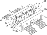
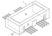
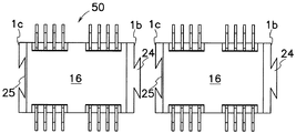
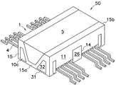
図1に示すように、本実施の形態の半導体発光ユニット(50)では、支持体(1)は、互いに対向して配置されて一対の光反射面(9)を形成する2つの側壁(15)と、側壁(15)に連絡し且つ光反射面(9)の間に支持面(3a)を形成する底壁(16)と、側壁(15)及び底壁(16)により支持体(1)の上面(1a)に形成される開口部(17)とを有する溝部(3)を備え、溝部(3)内に保護樹脂(5)が配置される。側壁(15)の長さ方向に沿う支持体(1)の溝部(3)の両端部(3b)に溝部(3)を開放する露出面(18)が形成される。支持体(1)の溝部(3)は、露出面(18)によって端部(3b)が延長される。即ち、図1に示す半導体発光ユニット(50)は、支持体(1)の幅方向の両端部(1c)に一対の側壁(15)を有するが、支持体(1)の長さ方向の少なくとも一方の端部(1b)に側壁を有さない点で、図15に示す半導体発光装置(51)とは異なる。 As shown in FIG. 1, in the semiconductor light emitting unit (50) of the present embodiment, the support (1) is disposed so as to face each other, and two side walls (15) forming a pair of light reflecting surfaces (9). ), A bottom wall (16) that communicates with the side wall (15) and forms a support surface (3a) between the light reflecting surfaces (9), and the support (1) by the side wall (15) and the bottom wall (16). ) Having a groove (3) having an opening (17) formed on the upper surface (1a), and a protective resin (5) is disposed in the groove (3). An exposed surface (18) that opens the groove (3) is formed at both ends (3b) of the groove (3) of the support (1) along the length direction of the side wall (15). The end (3b) of the groove (3) of the support (1) is extended by the exposed surface (18). That is, the semiconductor light emitting unit (50) shown in FIG. 1 has a pair of side walls (15) at both ends (1c) in the width direction of the support (1), but at least in the length direction of the support (1). This is different from the semiconductor light emitting device (51) shown in FIG. 15 in that one end (1b) does not have a side wall.
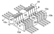
例示する半導体発光ユニット(50)では、支持体(1)は、上面(10a)に窪み部(12)を有する放熱板(10)と、窪み部(12)を除く放熱板(10)の上面(10a)及び一方の外側面(10b)を被覆する樹脂封止体(11)とを備える。樹脂封止体(11)は、放熱板(10)の窪み部(12)を形成する内部傾斜面(22)を上方に延長する傾斜部(13)を有し、放熱板(10)の窪み部(12)と樹脂封止体(11)の傾斜部(13)により、支持体(1)の溝部(3)が形成される。よって、放熱板(10)の窪み部(12)の底面がLEDチップ(2)を固着する支持面(3a)となり、LEDチップ(2)の下面電極と放熱板(10)とが電気的に接続される。放熱板(10)の窪み部(12)は、半導体発光ユニット(50)の幅方向に対向して一対の内部傾斜面(22)を有し、樹脂封止体(11)は、段差をもって異なる傾斜角度で窪み部(12)の内部傾斜面(22)を上方に延長する一対の傾斜部(13)を有する。放熱板(10)の窪み部(12)は、半導体発光ユニット(50)の長さ方向には内部傾斜面(22)を有さず、樹脂封止体(11)も傾斜部(13)を有さない。放熱板(10)は、例えば、銅、アルミニウム又はそれらの合金等の熱伝導率の高い金属により形成され、樹脂封止体(11)は、例えば、シリカ等のコンパウンド(充填材)の含有率が相対的に大きく且つ高軟化点を有する不透明又は半透明の樹脂により形成される。 In the illustrated semiconductor light emitting unit (50), the support (1) includes a heat sink (10) having a recess (12) on the upper surface (10a), and an upper surface of the heat sink (10) excluding the recess (12). (10a) and a resin sealing body (11) covering one outer surface (10b). The resin sealing body (11) has an inclined portion (13) extending upward from an internal inclined surface (22) that forms the recessed portion (12) of the heat sink (10), and the recess of the heat sink (10). The groove portion (3) of the support (1) is formed by the portion (12) and the inclined portion (13) of the resin sealing body (11). Therefore, the bottom surface of the recess (12) of the heat sink (10) serves as a support surface (3a) for fixing the LED chip (2), and the lower surface electrode of the LED chip (2) and the heat sink (10) are electrically connected. Connected. The recess (12) of the heat sink (10) has a pair of internal inclined surfaces (22) facing the width direction of the semiconductor light emitting unit (50), and the resin sealing body (11) is different with a step. It has a pair of inclined parts (13) which extend upward the internal inclined surface (22) of the hollow part (12) at an inclination angle. The recess (12) of the heat sink (10) does not have the internal inclined surface (22) in the length direction of the semiconductor light emitting unit (50), and the resin sealing body (11) also has the inclined portion (13). I don't have it. The heat radiating plate (10) is formed of a metal having a high thermal conductivity such as copper, aluminum or an alloy thereof, and the resin sealing body (11) is a content of a compound (filler) such as silica. Is relatively large and is formed of an opaque or translucent resin having a high softening point.
図5を参照するが、放熱板(10)の上面(10a)から一方の外側面(10b)にかけて絶縁体(6)を介して配線導体(4)が配置される。配線導体(4)は、LEDチップ(2)の上面電極に対して電気的に接続された一端(4a)と、樹脂封止体(11)から外部に延伸する他端(4b)とを有する。配線導体(4)の一端(4a)は、絶縁体(6)を介して放熱板(10)の上面(10a)に配置され、LEDチップ(2)の上面電極とリード細線(ボンディングワイヤ)(8)により接続される。樹脂封止体(11)は、放熱板(10)の上面(10a)及び一方の外側面(10b)と共に、配線導体(4)を被覆する。放熱板(10)の下面(10d)は、樹脂封止体(11)から外部に露出する。保護樹脂(5)は、例えば、光透過性の耐熱性シリコーン樹脂を溝部(3)内に充填して形成される。 Referring to FIG. 5, the wiring conductor (4) is disposed from the upper surface (10a) of the heat radiating plate (10) to the one outer surface (10b) through the insulator (6). The wiring conductor (4) has one end (4a) electrically connected to the upper surface electrode of the LED chip (2) and the other end (4b) extending outward from the resin sealing body (11). . One end (4a) of the wiring conductor (4) is disposed on the upper surface (10a) of the heat sink (10) via the insulator (6), and the upper surface electrode of the LED chip (2) and the lead wire (bonding wire) ( Connected by 8). The resin sealing body (11) covers the wiring conductor (4) together with the upper surface (10a) and one outer surface (10b) of the heat sink (10). The lower surface (10d) of the heat sink (10) is exposed to the outside from the resin sealing body (11). The protective resin (5) is formed, for example, by filling the groove (3) with a light transmissive heat resistant silicone resin.
図1に示すように、放熱板(10)は、一方の外側面(10b)から外側に突出し且つ樹脂封止体(11)に形成された切欠部(14)から外部に露出する突出部(26)を有する。放熱板(10)の一方の外側面(10b)が樹脂封止体(11)の切欠部(14)から外部に露出する突出部(26)を有するので、配線導体(4)及び放熱板(10)を通じてLEDチップ(2)に大電流を流して点灯させたときに、放熱板(10)の下面(10d)のみならず、放熱板(10)の突出部(26)からもLEDチップ(2)の熱を樹脂封止体(11)の外部に放出することができる。また、放熱板(10)の下面(10d)と配線導体(4)の他端(4b)とを回路基板に接続して、LEDチップ(2)の光の指向方向を回路基板に対して垂直とする平面実装の半導体発光ユニット(50)を構成すると共に、放熱板(10)の突出部(26)と配線導体(4)の他端(4b)とを回路基板に接続して、LEDチップ(2)の光の指向方向を回路基板に対して並行とする直立実装の半導体発光ユニット(50)を構成することができる。 As shown in FIG. 1, the heat radiating plate (10) protrudes outward from one outer surface (10b) and is exposed to the outside from a notch (14) formed in the resin sealing body (11). 26). Since one outer surface (10b) of the heat sink (10) has a protruding portion (26) exposed to the outside from the notch (14) of the resin sealing body (11), the wiring conductor (4) and the heat sink ( When the LED chip (2) is turned on with a large current through 10), the LED chip (not only from the lower surface (10d) of the heat sink (10) but also from the protrusion (26) of the heat sink (10) The heat of 2) can be released to the outside of the resin sealing body (11). Further, the lower surface (10d) of the heat sink (10) and the other end (4b) of the wiring conductor (4) are connected to the circuit board, and the light directing direction of the LED chip (2) is perpendicular to the circuit board. A flat-mount semiconductor light emitting unit (50) and connecting the protrusion (26) of the heat sink (10) and the other end (4b) of the wiring conductor (4) to the circuit board, The upright mounting semiconductor light emitting unit (50) in which the light directing direction (2) is parallel to the circuit board can be configured.
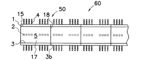
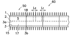
図2は、隣り合う半導体発光ユニット(50)の露出面(18)を互いに隣接して、複数の半導体発光ユニット(50)を直線状に組み合わせた線状光源(60)を示す。複数の半導体発光ユニット(50)を長さ方向に並置すると、隣り合う半導体発光ユニット(50)の保護樹脂(5)の端面が溝部(3)の端部(3b)で露出面(18)を介して隣接するので、LEDチップ(2)から放出される光が支持体(1)の側壁(15)により妨げられない。LEDチップ(2)から放出される光は、溝部(3)内の保護樹脂(5)を通じ、直接又は窪み部(12)の内部傾斜面(22)若しくは樹脂封止体(11)の傾斜部(13)に反射されて、支持体(1)の開口部(17)から放出される。また、LEDチップ(2)から放出される光の一部は、露出面(18)を介して隣接する半導体発光ユニット(50)の保護樹脂(5)を通じ、隣接する半導体発光ユニット(50)の開口部(17)から放出される。図3に示すように、LEDチップ(2)から放出される光(20)を支持体(1)の開口部(17)からのみならず、支持体(1)の露出面(18)から溝部(3)の端部(3b)方向にも放出して、複数の半導体発光ユニット(50)により構成される線状光源(60)の長さ方向に均一な光を外部に照射することができ、半導体発光ユニット(50)の間の輝度が低下する不具合の発生を抑制又は防止することができる。 FIG. 2 shows a linear light source (60) in which the exposed surfaces (18) of adjacent semiconductor light emitting units (50) are adjacent to each other and a plurality of semiconductor light emitting units (50) are linearly combined. When a plurality of semiconductor light emitting units (50) are juxtaposed in the longitudinal direction, the end surface of the protective resin (5) of the adjacent semiconductor light emitting unit (50) is the end portion (3b) of the groove portion (3) and the exposed surface (18). Therefore, the light emitted from the LED chip (2) is not blocked by the side wall (15) of the support (1). The light emitted from the LED chip (2) is directly or through the protective resin (5) in the groove (3), or the inner inclined surface (22) of the recess (12) or the inclined portion of the resin sealing body (11). Reflected by (13) and emitted from the opening (17) of the support (1). Further, part of the light emitted from the LED chip (2) passes through the protective resin (5) of the adjacent semiconductor light emitting unit (50) through the exposed surface (18), and then passes through the adjacent semiconductor light emitting unit (50). Released from the opening (17). As shown in FIG. 3, the light (20) emitted from the LED chip (2) is not only from the opening (17) of the support (1), but also from the exposed surface (18) of the support (1). It is also emitted in the direction of the end (3b) of (3), and uniform light can be emitted to the outside in the length direction of the linear light source (60) composed of a plurality of semiconductor light emitting units (50). In addition, it is possible to suppress or prevent the occurrence of a problem that the luminance between the semiconductor light emitting units (50) decreases.
本実施の形態の線状光源(60)では、線状光源(60)を構成する各半導体発光ユニット(50)は、放熱板(10)の下面(10d)を半田又はろう材により回路基板に接続して平面実装するか又は放熱板(10)の突出部(26)を半田又はろう材により回路基板に接続して直立実装することができる。よって、各半導体発光ユニット(50)を安定して回路基板に固着して、各半導体発光ユニット(50)の光の指向角度にバラツキが生じるのを防止することができる。線状光源(60)は、回路基板に対して垂直方向及び並行方向に線状光源(60)の長さ方向に均一な光を放出することができる。 In the linear light source (60) of the present embodiment, each semiconductor light emitting unit (50) constituting the linear light source (60) has a lower surface (10d) of the heat radiating plate (10) attached to a circuit board by solder or brazing material. It can be connected and mounted in a plane, or the protrusion (26) of the heat radiating plate (10) can be connected to the circuit board with solder or brazing material and mounted upright. Therefore, it is possible to stably fix each semiconductor light emitting unit (50) to the circuit board and prevent variations in the light directing angle of each semiconductor light emitting unit (50). The linear light source (60) can emit uniform light in the length direction of the linear light source (60) in a direction perpendicular to and parallel to the circuit board.
図2の線状光源(60)では、側壁(15)の長さ方向に沿う支持体(1)の溝部(3)の両端部(3b)に露出面(18)を設けたが、一方の端部(3b)のみに露出面(18)を設けてもよい。支持体(1)の溝部(3)の両端部(3b)に露出面(18)を設けると、1つの半導体発光ユニット(50)の両側にも他の半導体発光ユニット(50)を配置して少なくとも3つの半導体発光ユニット(50)により線状光源(60)を形成することができる。並置する半導体発光ユニット(50)の個数又は間隔を適宜変更して、所望の長さで光を外部に照射させることができる。 In the linear light source (60) of FIG. 2, the exposed surfaces (18) are provided at both ends (3b) of the groove (3) of the support (1) along the length direction of the side wall (15). The exposed surface (18) may be provided only at the end (3b). When exposed surfaces (18) are provided at both ends (3b) of the groove (3) of the support (1), other semiconductor light emitting units (50) are arranged on both sides of one semiconductor light emitting unit (50). The linear light source (60) can be formed by at least three semiconductor light emitting units (50). By appropriately changing the number or interval of the semiconductor light emitting units (50) juxtaposed, the light can be irradiated to the outside with a desired length.
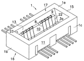
図1の半導体発光ユニット(50)を製造する際に、複数の放熱板(10)及び配線導体(4)がプレス加工によって帯状金属からそれぞれ形成される。図4に示すように、配線導体(4)は、他端(4b)に形成された連結部材(19)により互いに連結されている。次に、図5に示すように、例えば、テープ状の絶縁体(6)が放熱板(10)の上面(10a)及び一方の外側面(10b)に貼着され、折曲された配線導体(4)が配置される。続いて、周知のインジェクションモールド法により、図6に示すように、放熱板(10)の上面(10a)、一方の外側面(10b)及び配線導体(4)を被覆する樹脂封止体(11)が形成される。この工程により、4つの側壁(15)と、側壁(15)に連絡し且つ光反射面(9)の間に支持面(3a)を形成する底壁(16)と、側壁(15)及び底壁(16)により上部に形成された開口部(17)とを備えた凹部(23)を有する支持体(1)が形成される。樹脂封止体(11)を形成する工程の前又は後に、支持体(1)の開口部(17)を通じて支持体(1)の支持面(3a)にLEDチップ(2)を固着する。ダイボンダを使用して放熱板(10)の窪み部(12)の底面にLEDチップ(2)を固着し、周知のワイヤボンディング法によってLEDチップ(2)の上部電極と配線導体(4)の一端(4a)とをリード細線(8)により接続する。 When the semiconductor light emitting unit (50) of FIG. 1 is manufactured, a plurality of heat radiating plates (10) and wiring conductors (4) are each formed from a strip metal by pressing. As shown in FIG. 4, the wiring conductor (4) is mutually connected by the connection member (19) formed in the other end (4b). Next, as shown in FIG. 5, for example, a tape-like insulator (6) is attached to the upper surface (10a) and one outer surface (10b) of the heat sink (10), and the wiring conductor is bent. (4) is arranged. Subsequently, as shown in FIG. 6, a resin sealing body (11) covering the upper surface (10a) of the heat radiating plate (10), one outer surface (10b) and the wiring conductor (4) by a known injection molding method. ) Is formed. By this step, the four side walls (15), the bottom wall (16) communicating with the side walls (15) and forming the support surface (3a) between the light reflecting surfaces (9), the side walls (15) and the bottom A support (1) having a recess (23) with an opening (17) formed in the upper part by a wall (16) is formed. Before or after the step of forming the resin sealing body (11), the LED chip (2) is fixed to the support surface (3a) of the support (1) through the opening (17) of the support (1). The LED chip (2) is fixed to the bottom surface of the recess (12) of the heat sink (10) using a die bonder, and the upper electrode of the LED chip (2) and one end of the wiring conductor (4) by a well-known wire bonding method. Connect (4a) to the lead wire (8).
次に、ディスペンサにより、凹部(23)内に保護樹脂(5)を充填してLEDチップ(2)を封止する。図7に示すように、支持体(1)の凹部(23)は、4つの側壁(15)と底壁(16)により形成された容器形状を有するので、保護樹脂(5)を支持体(1)の凹部(23)内に保持することができる。支持体(1)の凹部(23)内の保護樹脂(5)が硬化した後に、図7に破線で示すように、支持体(1)の両端部(1b)を切断して、保護樹脂(5)を外部に露出する露出面(18)を有する溝部(3)を支持体(1)に形成する。この後、配線導体(4)から連結部材(19)等の不要な部分を除去して図1に示す完成した半導体発光ユニット(50)が得られる。 Next, the concave resin (23) is filled with the protective resin (5) by a dispenser to seal the LED chip (2). As shown in FIG. 7, since the recess (23) of the support (1) has a container shape formed by four side walls (15) and a bottom wall (16), the protective resin (5) is attached to the support ( It can be held in the recess (23) of 1). After the protective resin (5) in the concave portion (23) of the support (1) is cured, as shown by a broken line in FIG. 7, both ends (1b) of the support (1) are cut and the protective resin ( A groove (3) having an exposed surface (18) exposing 5) to the outside is formed in the support (1). Thereafter, unnecessary portions such as the connecting member (19) are removed from the wiring conductor (4) to obtain the completed semiconductor light emitting unit (50) shown in FIG.
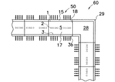
本発明の実施の形態は、前記の実施の形態に限定されず、種々の変更が可能である。例えば、図8に示すように、支持体(1)の支持面(3a)に複数のLEDチップ(2)を等間隔で配置してもよい。半導体発光ユニット(50)は、長さ方向により均一な光を放出することができる。また、並置される半導体発光ユニット(50)の各端部に配置された隣接する2つのLEDチップ(2)の間隔L1を各半導体発光ユニット(50)の他のLEDチップ(2)の間隔L2と同一間隔としてもよい。線状光源(60)は、長さ方向により均一な光を放出することができる。図9に示すように、半導体発光ユニット(50)の側壁(15)の長さ方向の一方の端部(15a)に端部側壁(27)を形成してもよい。線状光源(60)の端部に配置される半導体発光ユニット(50)に端部側壁(27)を設けて、線状光源(60)の端部の光の拡散を防止することができる。図10に示すように、複数の半導体発光ユニット(50)をL字型に配置してもよい。その際、横方向に配列された半導体発光ユニット(50)と縦方向に配列された半導体発光ユニット(50)との間に接続部材(28)を設けてもよい。接続部材(28)は、L字状又は扇状に形成され且つ半導体発光ユニット(50)の側壁(15)と隣接して配置される側壁(29)を有し、L字型に配置された線状光源(60)の角部の光の拡散を防止することができる。図示しないが、接続部材(28)の代わりにL字状又は扇状に形成された半導体発光ユニットを配置してもよい。 Embodiments of the present invention are not limited to the above-described embodiments, and various modifications can be made. For example, as shown in FIG. 8, a plurality of LED chips (2) may be arranged at equal intervals on the support surface (3a) of the support (1). The semiconductor light emitting unit (50) can emit more uniform light in the length direction. Further, the distance L 1 between two adjacent LED chips (2) arranged at each end of the semiconductor light emitting units (50) arranged side by side is the distance between the other LED chips (2) of each semiconductor light emitting unit (50). L 2 and may be the same interval. The linear light source (60) can emit more uniform light in the length direction. As shown in FIG. 9, an end side wall (27) may be formed at one end (15a) in the length direction of the side wall (15) of the semiconductor light emitting unit (50). An end side wall (27) can be provided in the semiconductor light emitting unit (50) disposed at the end of the linear light source (60) to prevent the diffusion of light at the end of the linear light source (60). As shown in FIG. 10, a plurality of semiconductor light emitting units (50) may be arranged in an L shape. At that time, a connecting member (28) may be provided between the semiconductor light emitting units (50) arranged in the horizontal direction and the semiconductor light emitting units (50) arranged in the vertical direction. The connecting member (28) has a side wall (29) formed in an L shape or a fan shape and disposed adjacent to the side wall (15) of the semiconductor light emitting unit (50), and is arranged in an L shape. The diffusion of light at the corner of the light source (60) can be prevented. Although not shown, a semiconductor light emitting unit formed in an L shape or a fan shape may be arranged instead of the connection member (28).
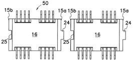
複数の半導体発光ユニット(50)の連結を容易にする連結部(24,25)を各半導体発光ユニット(50)の側面に形成してもよい。例えば、図11に示すように、半導体発光ユニット(50)の各側壁(15)の長さ方向の一方の端部(15a)に連結凸部(24)を設け、各側壁(15)の長さ方向の他方の端部(15b)に連結凸部(24)に嵌合する連結凹部(25)を設ける。隣り合う半導体発光ユニット(50)の端部(15a,15b)に形成された連結凸部(24)と連結凹部(25)とを互いに嵌合させることにより、所定の位置への複数の半導体発光ユニット(50)の位置決めが容易となると同時に、誤って一方の端部(15a)同士又は他方の端部(15b)同士を接合する誤装着を防止することができる。連結凸部(24)の外周面及び連結凹部(25)の内周面は、図12に示すように、半導体発光ユニット(50)を接続する方向に対して平行に形成してもよいが、図13に示すように、半導体発光ユニット(50)を接続する方向に対して傾斜して形成してもよい。図13の半導体発光ユニット(50)によれば、導体発光ユニット(50)同士を強固に接合して線状光源(60)を組み立てることができる。 Connection portions (24, 25) that facilitate connection of the plurality of semiconductor light emitting units (50) may be formed on the side surfaces of each semiconductor light emitting unit (50). For example, as shown in FIG. 11, a connecting projection (24) is provided at one end (15a) in the length direction of each side wall (15) of the semiconductor light emitting unit (50), and the length of each side wall (15) is increased. A connecting recess (25) that fits into the connecting protrusion (24) is provided at the other end (15b) in the vertical direction. A plurality of semiconductor light emitting devices in a predetermined position can be obtained by fitting the connecting convex portions (24) and the connecting concave portions (25) formed at the ends (15a, 15b) of the adjacent semiconductor light emitting units (50). Positioning of the unit (50) is facilitated, and at the same time, it is possible to prevent erroneous mounting that erroneously joins one end (15a) or the other end (15b). The outer peripheral surface of the connecting convex portion (24) and the inner peripheral surface of the connecting concave portion (25) may be formed in parallel to the direction in which the semiconductor light emitting unit (50) is connected, as shown in FIG. As shown in FIG. 13, the semiconductor light emitting unit (50) may be formed inclined with respect to the connecting direction. According to the semiconductor light emitting unit (50) of FIG. 13, the conductor light emitting units (50) can be firmly joined together to assemble the linear light source (60).
図14に示す半導体発光ユニット(50)では、放熱板(10)は、他方の外側面(10c)から外側に突出し且つ樹脂封止体(11)に形成された切欠部(31)から外部に露出する突出部(32)を有する。図14の半導体発光ユニット(50)によれば、LEDチップ(2)から放熱板(10)に伝達された熱を放熱板(10)の下面(10d)及び突出部(26)のみならず、突出部(32)からも樹脂封止体(11)の外部に放出することができる。また、側壁(15)の端部(15a,15b)にそれぞれ突出部(32)を有するので、複数の半導体発光ユニット(50)の隣接する突出部(32)を半田又はろう材により固着して、半導体発光ユニット(50)を連結することができる。図14の半導体発光ユニット(50)を直線状に組み合わせた線状光源(60)によれば、複数の半導体発光ユニット(50)の放熱板(10)を電気的に接続して、各半導体発光ユニット(50)を同時に点灯させることができる。 In the semiconductor light emitting unit (50) shown in FIG. 14, the heat radiating plate (10) protrudes outward from the other outer surface (10c) and extends outwardly from a notch (31) formed in the resin sealing body (11). It has an exposed protrusion (32). According to the semiconductor light emitting unit (50) of FIG. 14, not only the heat transferred from the LED chip (2) to the heat sink (10) but also the lower surface (10d) and the protrusion (26) of the heat sink (10), It can also discharge | release to the exterior of the resin sealing body (11) from a protrusion part (32). Further, since each of the end portions (15a, 15b) of the side wall (15) has a protrusion (32), the adjacent protrusions (32) of the plurality of semiconductor light emitting units (50) are fixed with solder or brazing material. The semiconductor light emitting unit (50) can be connected. According to the linear light source (60) in which the semiconductor light emitting units (50) of FIG. 14 are linearly combined, the heat radiation plates (10) of the plurality of semiconductor light emitting units (50) are electrically connected to each other to emit light from each semiconductor. Unit (50) can be lit at the same time.
上記実施の形態では、支持体(1)に容器形状の凹部(23)を形成した後に、凹部(23)の両端部を切断して、保護樹脂(5)が充填された溝部(3)を支持体(1)に形成したが、支持体(1)に凹部(23)を形成せずに、溝部(3)を形成してもよい。図示しないが、放熱板(10)の他方の外側面(10c)を成形型の内面に密着させた状態でインジェクションモールド法により放熱板(10)の上面(10a)、一方の外側面(10b)及び配線導体(4)を被覆する樹脂封止体(11)を形成する。この工程により、2つの側壁(15)と、側壁(15)に連絡し且つ光反射面(9)の間に支持面(3a)を形成する底壁(16)と、側壁(15)及び底壁(16)により上部に形成された開口部(17)とを備えた側壁(15)の長さ方向に沿う溝部(3)を有する支持体(1)が形成される。樹脂封止体(11)を形成する工程の前又は後に、支持体(1)の支持面(3a)にLEDチップ(2)を固着すると共に、LEDチップ(2)の上部電極と配線導体(4)の一端(4a)とをリード細線(8)により接続する。次に、支持体(1)を支持台上に配置して、支持台の可動壁により支持体(1)の露出面(18)を覆い、溝部(3)内に光透過性の保護樹脂(5)を充填してLEDチップ(2)を封止する。保護樹脂(5)が硬化した後に、支持台から支持体(1)を取り出して、保護樹脂(5)を外部に露出する露出面(18)を有する溝部(3)を支持体(1)に形成する。この後、配線導体(4)から不要な部分を除去して図1に示す完成した半導体発光ユニット(50)が得られる。 In the above embodiment, after forming the container-shaped recess (23) on the support (1), both ends of the recess (23) are cut to form the groove (3) filled with the protective resin (5). Although formed on the support (1), the groove (3) may be formed without forming the recess (23) on the support (1). Although not shown, the upper surface (10a) of the heat radiating plate (10) and one outer surface (10b) of the heat radiating plate (10) by the injection molding method with the other outer surface (10c) of the heat radiating plate (10) being in close contact with the inner surface of the mold. And the resin sealing body (11) which covers the wiring conductor (4) is formed. By this step, two side walls (15), a bottom wall (16) that communicates with the side walls (15) and forms a support surface (3a) between the light reflecting surfaces (9), and the side walls (15) and bottom A support (1) having a groove (3) along the length direction of a side wall (15) provided with an opening (17) formed in the upper part by the wall (16) is formed. Before or after the step of forming the resin sealing body (11), the LED chip (2) is fixed to the support surface (3a) of the support body (1), and the upper electrode and the wiring conductor ( Connect one end (4a) of 4) with a fine lead wire (8). Next, the support (1) is placed on the support base, the exposed surface (18) of the support (1) is covered by the movable wall of the support base, and a light-transmitting protective resin ( 5) is filled to seal the LED chip (2). After the protective resin (5) is cured, the support (1) is taken out of the support base, and the groove (3) having an exposed surface (18) exposing the protective resin (5) to the outside is formed on the support (1). Form. Thereafter, unnecessary portions are removed from the wiring conductor (4) to obtain the completed semiconductor light emitting unit (50) shown in FIG.
半導体発光ユニット(50)は、8個のLEDチップ(2)及びLEDチップ(2)を挟んで16本の配線導体(4)が備えられるが、これらの構成は適宜に変更してよく、青色、赤色及び緑色等の単色又は複数色のLEDチップ(2)により半導体発光ユニット(50)を構成してもよい。本実施の形態の半導体発光ユニット(50)によれば、隣接する半導体発光ユニット(50)の間で良好に混色した光を放出できる。保護樹脂(5)に蛍光物質を混入して、LEDチップ(2)から照射される光の波長を変換させてもよい。半導体発光ユニット(50)は、各配線導体(4)を通じて電流を流して複数のLEDチップ(2)を個別に点灯させることができる。しかしながら、各配線導体(4)を一体に形成して、複数のLEDチップ(2)を一度に点灯させてもよい。例示する半導体発光ユニット(50)では、支持体(1)は、金属製の放熱板(10)及び樹脂封止体(11)により構成したが、支持体(1)を金属又は樹脂の何れか一方により一体に形成してもよい。本実施の形態の半導体発光ユニット(50)に適用した半導体発光装置の基本構造は、特許文献1により公知であり、本発明を限定するものではない。
The semiconductor light emitting unit (50) includes eight LED chips (2) and sixteen wiring conductors (4) sandwiching the LED chip (2), but these configurations may be changed as appropriate. The semiconductor light emitting unit (50) may be composed of LED chips (2) of single color or multiple colors such as red and green. According to the semiconductor light emitting unit (50) of the present embodiment, it is possible to emit light that is well mixed between adjacent semiconductor light emitting units (50). A fluorescent substance may be mixed in the protective resin (5) to convert the wavelength of light emitted from the LED chip (2). The semiconductor light emitting unit (50) can turn on the plurality of LED chips (2) individually by passing a current through each wiring conductor (4). However, the respective wiring conductors (4) may be formed integrally and the plurality of LED chips (2) may be lit at a time. In the illustrated semiconductor light emitting unit (50), the support (1) is composed of a metal heat sink (10) and a resin sealing body (11), but the support (1) is either metal or resin. One may be formed integrally. The basic structure of the semiconductor light emitting device applied to the semiconductor light emitting unit (50) of the present embodiment is known from
本発明は、各種表示装置のバックライト、LEDディスプレイ装置、照明装置又はプリンタ、ファックシミリ若しくはスキャナのラインセンサ等に使用される線状光源に良好に適用できる。 The present invention can be favorably applied to linear light sources used for backlights of various display devices, LED display devices, illumination devices or printers, line sensors of scanners, scanners, and the like.
(1)・・支持体、 (2)・・LEDチップ(半導体発光素子)、 (3)・・溝部、 (3a)・・支持面、 (3b)・・一方の端部、 (5)・・保護樹脂、 (9)・・光反射面、 (15)・・側壁、 (15a)・・一方の端部、 (16)・・底壁、 (17)・・開口部、 (18)・・露出面、 (23)・・凹部、 (24)・・連結凸部、 (25)・・連結凹部、 (50)・・半導体発光ユニット、 (1) ・ ・ Support, (2) ・ ・ LED chip (semiconductor light emitting device), (3) ・ ・ Groove, (3a) ・ ・ Support surface, (3b) ・ ・ One end, (5) ・・ Protective resin, (9) ・ ・ Light reflecting surface, (15) ・ ・ Side wall, (15a) ・ ・ One end, (16) ・ ・ Bottom wall, (17) ・ ・ Opening, (18) ・・ Exposed surface, (23) ・ ・ Recess, (24) ・ ・ Connecting protrusion, (25) ・ ・ Connecting recess, (50) ・ ・ Semiconductor light-emitting unit,
Claims (8)
前記支持体は、互いに対向して配置されて一対の光反射面を形成する側壁と、該側壁に連絡し且つ前記光反射面の間に支持面を形成する底壁と、前記側壁及び底壁により上部に形成される開口部とを有する溝部を備え、
前記半導体発光素子は、前記支持体の支持面に固着され、
前記保護樹脂は、前記溝部内に配置され、
前記側壁の長さ方向に沿う前記支持体の溝部の少なくとも一方の端部に前記溝部を開放する露出面を設けたことを特徴する半導体発光ユニット。 A support, a semiconductor light emitting device fixed on the support, and a light-transmitting protective resin for sealing the semiconductor light emitting device,
The support body is disposed to face each other to form a pair of light reflecting surfaces, a bottom wall that communicates with the side walls and forms a support surface between the light reflecting surfaces, and the side walls and the bottom wall. A groove having an opening formed in the upper portion by
The semiconductor light emitting element is fixed to a support surface of the support,
The protective resin is disposed in the groove,
A semiconductor light emitting unit, wherein an exposed surface that opens the groove is provided at at least one end of the groove of the support body along the length direction of the side wall.
前記支持体は、対向して配置されて一対の光反射面を形成する側壁と、該側壁に連絡し且つ前記光反射面の間に支持面を形成する底壁と、前記側壁及び底壁により上部に形成される開口部とを有する溝部を備え、
前記半導体発光素子は、前記支持体の支持面に固着され、
前記保護樹脂は、前記溝部内に配置され、
前記側壁の長さ方向に沿う前記支持体の溝部の少なくとも一方の端部に前記溝部を開放する露出面を設け、
隣り合う前記半導体発光ユニットの露出面を互いに隣接させたことを特徴とする線状光源。 A plurality of semiconductor light-emitting units having a support, a semiconductor light-emitting element fixed on the support, and a light-transmitting protective resin for sealing the semiconductor light-emitting element are linearly combined,
The support includes a side wall that is disposed opposite to form a pair of light reflection surfaces, a bottom wall that communicates with the side walls and forms a support surface between the light reflection surfaces, and the side walls and the bottom wall. A groove having an opening formed in the upper portion;
The semiconductor light emitting element is fixed to a support surface of the support,
The protective resin is disposed in the groove,
An exposed surface that opens the groove is provided on at least one end of the groove of the support along the length direction of the side wall;
A linear light source, wherein exposed surfaces of adjacent semiconductor light emitting units are adjacent to each other.
少なくとも3つの前記半導体発光ユニットを直線状に組み合わせた請求項4に記載の線状光源。 Providing the exposed surface at both ends of the groove of the support body along the length direction of the side wall;
The linear light source according to claim 4, wherein at least three of the semiconductor light emitting units are linearly combined.
前記支持体の開口部を通じて前記支持体の支持面に半導体発光素子を固着する工程と、
前記支持体を支持台上に配置して、前記支持体の露出面を覆い、前記溝部内に光透過性の保護樹脂を充填して前記半導体発光素子を封止する工程と、
前記保護樹脂の硬化後に、前記支持台から前記支持体を取り出す工程とを含むことを特徴とする半導体発光ユニットの製法。 A side wall that is disposed opposite to each other to form a pair of light reflecting surfaces, a bottom wall that communicates with the side walls and forms a support surface between the light reflecting surfaces, and an upper portion formed by the side walls and the bottom wall. Forming a support having a groove portion along the length direction of the side wall provided with an opening, and having an exposed surface that opens the groove portion at at least one end of the groove portion;
Fixing the semiconductor light emitting element to the support surface of the support through the opening of the support;
Placing the support on a support base, covering the exposed surface of the support, filling the groove with a light-transmitting protective resin, and sealing the semiconductor light emitting element;
And a step of removing the support from the support after the protective resin is cured.
前記支持体の開口部を通じて前記支持体の支持面に半導体発光素子を固着する工程と、
前記凹部内に光透過性の保護樹脂を充填して前記半導体発光素子を封止する工程と、
前記保護樹脂が硬化した後に、前記支持体の少なくとも一方の端部を切断して、前記保護樹脂を外部に露出する露出面を有する溝部を前記支持体に形成する工程とを含むことを特徴とする半導体発光ユニットの製法。 A recess comprising: a side wall forming a light reflecting surface; a bottom wall communicating with the side wall and forming a support surface between the light reflecting surfaces; and an opening formed at an upper portion by the side wall and the bottom wall. Forming a support having:
Fixing the semiconductor light emitting element to the support surface of the support through the opening of the support;
A step of sealing the semiconductor light emitting element by filling a light-transmitting protective resin in the recess;
Cutting the at least one end of the support after the protective resin is cured, and forming a groove on the support having an exposed surface that exposes the protective resin to the outside. Manufacturing method of semiconductor light emitting unit.
Priority Applications (2)
| Application Number | Priority Date | Filing Date | Title |
|---|---|---|---|
| JP2006014992A JP4967347B2 (en) | 2006-01-24 | 2006-01-24 | Manufacturing method of linear light source and semiconductor light emitting unit |
| US11/657,681 US7821025B2 (en) | 2006-01-24 | 2007-01-23 | Semiconductor light emitting unit, method for manufacturing same and linear light source |
Applications Claiming Priority (1)
| Application Number | Priority Date | Filing Date | Title |
|---|---|---|---|
| JP2006014992A JP4967347B2 (en) | 2006-01-24 | 2006-01-24 | Manufacturing method of linear light source and semiconductor light emitting unit |
Publications (2)
| Publication Number | Publication Date |
|---|---|
| JP2007200974A true JP2007200974A (en) | 2007-08-09 |
| JP4967347B2 JP4967347B2 (en) | 2012-07-04 |
Family
ID=38284645
Family Applications (1)
| Application Number | Title | Priority Date | Filing Date |
|---|---|---|---|
| JP2006014992A Expired - Fee Related JP4967347B2 (en) | 2006-01-24 | 2006-01-24 | Manufacturing method of linear light source and semiconductor light emitting unit |
Country Status (2)
| Country | Link |
|---|---|
| US (1) | US7821025B2 (en) |
| JP (1) | JP4967347B2 (en) |
Cited By (3)
| Publication number | Priority date | Publication date | Assignee | Title |
|---|---|---|---|---|
| WO2009060676A1 (en) * | 2007-11-06 | 2009-05-14 | Sanken Electric Co., Ltd. | Semiconductor light emitting devices, composite light emitting device wherein the semiconductor light emitting devices are arranged, and planar light emitting source using the composite light emitting device |
| US8641256B2 (en) | 2007-11-06 | 2014-02-04 | Sanken Electric Co., Ltd. | Semiconductor light emitting device, composite light emitting device with arrangement of semiconductor light emitting devices, and planar light source using composite light emitting device |
| JP2016029739A (en) * | 2010-09-06 | 2016-03-03 | ヘレーウス ノーブルライト ゲゼルシャフト ミット ベシュレンクテルハフツングHeraeus Noblelight GmbH | Coating method for optoelectronic chip-on-board module |
Families Citing this family (2)
| Publication number | Priority date | Publication date | Assignee | Title |
|---|---|---|---|---|
| DE102008021618A1 (en) * | 2007-11-28 | 2009-06-04 | Osram Opto Semiconductors Gmbh | Chip arrangement, connection arrangement, LED and method for producing a chip arrangement |
| KR102143890B1 (en) * | 2013-10-15 | 2020-08-12 | 온세미컨덕터코리아 주식회사 | Power module package and method for manufacturing the same |
Citations (5)
| Publication number | Priority date | Publication date | Assignee | Title |
|---|---|---|---|---|
| JPS6022853U (en) * | 1983-07-23 | 1985-02-16 | 持田製薬株式会社 | LED lamps that can be connected closely |
| JPH10308536A (en) * | 1997-05-06 | 1998-11-17 | Mitsubishi Cable Ind Ltd | LED line light source |
| JP2004296882A (en) * | 2003-03-27 | 2004-10-21 | Sanken Electric Co Ltd | Semiconductor light emitting device |
| JP2005285899A (en) * | 2004-03-29 | 2005-10-13 | Kawaguchiko Seimitsu Co Ltd | Light emitting diode package structure |
| JP2006210627A (en) * | 2005-01-27 | 2006-08-10 | Kyocera Corp | Light emitting element storage package, light emitting device, and lighting device |
Family Cites Families (3)
| Publication number | Priority date | Publication date | Assignee | Title |
|---|---|---|---|---|
| US6170963B1 (en) * | 1998-03-30 | 2001-01-09 | Eastman Kodak Company | Light source |
| JP2000091646A (en) | 1998-09-17 | 2000-03-31 | Oki Electric Ind Co Ltd | Led array |
| CN102290409B (en) * | 2003-04-01 | 2014-01-15 | 夏普株式会社 | Light-emitting apparatus |
-
2006
- 2006-01-24 JP JP2006014992A patent/JP4967347B2/en not_active Expired - Fee Related
-
2007
- 2007-01-23 US US11/657,681 patent/US7821025B2/en not_active Expired - Fee Related
Patent Citations (5)
| Publication number | Priority date | Publication date | Assignee | Title |
|---|---|---|---|---|
| JPS6022853U (en) * | 1983-07-23 | 1985-02-16 | 持田製薬株式会社 | LED lamps that can be connected closely |
| JPH10308536A (en) * | 1997-05-06 | 1998-11-17 | Mitsubishi Cable Ind Ltd | LED line light source |
| JP2004296882A (en) * | 2003-03-27 | 2004-10-21 | Sanken Electric Co Ltd | Semiconductor light emitting device |
| JP2005285899A (en) * | 2004-03-29 | 2005-10-13 | Kawaguchiko Seimitsu Co Ltd | Light emitting diode package structure |
| JP2006210627A (en) * | 2005-01-27 | 2006-08-10 | Kyocera Corp | Light emitting element storage package, light emitting device, and lighting device |
Cited By (3)
| Publication number | Priority date | Publication date | Assignee | Title |
|---|---|---|---|---|
| WO2009060676A1 (en) * | 2007-11-06 | 2009-05-14 | Sanken Electric Co., Ltd. | Semiconductor light emitting devices, composite light emitting device wherein the semiconductor light emitting devices are arranged, and planar light emitting source using the composite light emitting device |
| US8641256B2 (en) | 2007-11-06 | 2014-02-04 | Sanken Electric Co., Ltd. | Semiconductor light emitting device, composite light emitting device with arrangement of semiconductor light emitting devices, and planar light source using composite light emitting device |
| JP2016029739A (en) * | 2010-09-06 | 2016-03-03 | ヘレーウス ノーブルライト ゲゼルシャフト ミット ベシュレンクテルハフツングHeraeus Noblelight GmbH | Coating method for optoelectronic chip-on-board module |
Also Published As
| Publication number | Publication date |
|---|---|
| US7821025B2 (en) | 2010-10-26 |
| US20070170416A1 (en) | 2007-07-26 |
| JP4967347B2 (en) | 2012-07-04 |
Similar Documents
| Publication | Publication Date | Title |
|---|---|---|
| JP4174823B2 (en) | Semiconductor light emitting device | |
| JP5295107B2 (en) | LIGHT EMITTING DIODE PACKAGE USING LEAD FRAME HAVING HEAT SINK SUPPORTING UNIT AND METHOD FOR MANUFACTURING THE LIGHT EMITTING DIODE PACKAGE | |
| JP3798195B2 (en) | Chip type light emitting device | |
| US20040173810A1 (en) | Light emitting diode package structure | |
| US8749136B2 (en) | Light emitting apparatus and light unit | |
| JP2011146709A (en) | Light-emitting device and illumination system | |
| KR101659355B1 (en) | Light-emitting element package | |
| JP2005150624A (en) | Lead frame for semiconductor device and surface light emitting device using the same | |
| WO2006104325A1 (en) | Light emitting diode structure | |
| JP2008147203A (en) | Semiconductor light emitting device | |
| JP2008218764A (en) | Light emitting device | |
| US8791482B2 (en) | Light emitting device package | |
| JP4967347B2 (en) | Manufacturing method of linear light source and semiconductor light emitting unit | |
| KR20110013401A (en) | LED package, lead frame and its manufacturing method | |
| JP4938255B2 (en) | Light emitting element storage package, light source, and light emitting device | |
| US20120074456A1 (en) | Light emitting device package | |
| JP3128379U (en) | Flip layer structure for LED package | |
| JP4659515B2 (en) | Light-emitting element mounting substrate, light-emitting element storage package, light-emitting device, and lighting device | |
| JP4679917B2 (en) | Semiconductor light emitting device | |
| KR20110125067A (en) | The light- | |
| JP6064415B2 (en) | Light emitting device | |
| KR101781043B1 (en) | Light-emitting element array | |
| JP6038528B2 (en) | Light emitting device | |
| KR101346706B1 (en) | Light emitting device | |
| JP2006041379A (en) | Light source device |
Legal Events
| Date | Code | Title | Description |
|---|---|---|---|
| A621 | Written request for application examination |
Free format text: JAPANESE INTERMEDIATE CODE: A621 Effective date: 20081210 |
|
| A977 | Report on retrieval |
Free format text: JAPANESE INTERMEDIATE CODE: A971007 Effective date: 20110427 |
|
| A131 | Notification of reasons for refusal |
Free format text: JAPANESE INTERMEDIATE CODE: A131 Effective date: 20110510 |
|
| A521 | Request for written amendment filed |
Free format text: JAPANESE INTERMEDIATE CODE: A523 Effective date: 20110707 |
|
| A131 | Notification of reasons for refusal |
Free format text: JAPANESE INTERMEDIATE CODE: A131 Effective date: 20111004 |
|
| A521 | Request for written amendment filed |
Free format text: JAPANESE INTERMEDIATE CODE: A523 Effective date: 20111130 |
|
| TRDD | Decision of grant or rejection written | ||
| A01 | Written decision to grant a patent or to grant a registration (utility model) |
Free format text: JAPANESE INTERMEDIATE CODE: A01 Effective date: 20120306 |
|
| A01 | Written decision to grant a patent or to grant a registration (utility model) |
Free format text: JAPANESE INTERMEDIATE CODE: A01 |
|
| A61 | First payment of annual fees (during grant procedure) |
Free format text: JAPANESE INTERMEDIATE CODE: A61 Effective date: 20120319 |
|
| FPAY | Renewal fee payment (event date is renewal date of database) |
Free format text: PAYMENT UNTIL: 20150413 Year of fee payment: 3 |
|
| R150 | Certificate of patent or registration of utility model |
Free format text: JAPANESE INTERMEDIATE CODE: R150 |
|
| R250 | Receipt of annual fees |
Free format text: JAPANESE INTERMEDIATE CODE: R250 |
|
| R250 | Receipt of annual fees |
Free format text: JAPANESE INTERMEDIATE CODE: R250 |
|
| LAPS | Cancellation because of no payment of annual fees |