JP2007201224A - Semiconductor device - Google Patents
Semiconductor device Download PDFInfo
- Publication number
- JP2007201224A JP2007201224A JP2006018650A JP2006018650A JP2007201224A JP 2007201224 A JP2007201224 A JP 2007201224A JP 2006018650 A JP2006018650 A JP 2006018650A JP 2006018650 A JP2006018650 A JP 2006018650A JP 2007201224 A JP2007201224 A JP 2007201224A
- Authority
- JP
- Japan
- Prior art keywords
- liquid
- semiconductor module
- semiconductor
- cooling member
- semiconductor device
- Prior art date
- Legal status (The legal status is an assumption and is not a legal conclusion. Google has not performed a legal analysis and makes no representation as to the accuracy of the status listed.)
- Pending
Links
Images





Classifications
-
- H—ELECTRICITY
- H05—ELECTRIC TECHNIQUES NOT OTHERWISE PROVIDED FOR
- H05K—PRINTED CIRCUITS; CASINGS OR CONSTRUCTIONAL DETAILS OF ELECTRIC APPARATUS; MANUFACTURE OF ASSEMBLAGES OF ELECTRICAL COMPONENTS
- H05K7/00—Constructional details common to different types of electric apparatus
- H05K7/20—Modifications to facilitate cooling, ventilating, or heating
- H05K7/2089—Modifications to facilitate cooling, ventilating, or heating for power electronics, e.g. for inverters for controlling motor
- H05K7/20927—Liquid coolant without phase change
Landscapes
- Cooling Or The Like Of Semiconductors Or Solid State Devices (AREA)
Abstract
【課題】装置の小型化を損なわず簡単な構成でもって、半導体モジュールのシール部分から液漏れが生じても電極端子が短絡するなどの不具合が生じるのを確実に防止することができる半導体装置を提供する。
【解決手段】半導体素子が実装された半導体モジュール1と液冷部材2とを有し、半導体モジュール1の冷却面が液冷部材2に形成された流通路20の開口部21に臨むとともに、その開口部21周縁と半導体モジュール1の周縁とがシール部材3を介在させて接合され、また、半導体モジュール1にはその電極端子11,12とシール部材3との間に位置し、かつ、液冷部材2との接合面と略直交する側面19の外方に向けて張り出した防液壁4が一体的に設けられている。
【選択図】図1A semiconductor device having a simple configuration that does not impair the downsizing of the device, and can reliably prevent problems such as short-circuiting of electrode terminals even when liquid leakage occurs from a seal portion of a semiconductor module. provide.
A semiconductor module having a semiconductor element mounted thereon and a liquid cooling member. The cooling surface of the semiconductor module faces the opening of a flow passage formed in the liquid cooling member. The periphery of the opening 21 and the periphery of the semiconductor module 1 are joined with the seal member 3 interposed therebetween. The semiconductor module 1 is located between the electrode terminals 11 and 12 and the seal member 3 and is liquid-cooled. A liquid-proof wall 4 projecting toward the outside of the side surface 19 substantially orthogonal to the joint surface with the member 2 is integrally provided.
[Selection] Figure 1
Description
この発明は、発熱量の大きな半導体素子を備えた半導体モジュールを冷却する機能を備えた半導体装置に係り、特には、半導体モジュールを冷却液によって直接に冷却する直接液冷方式の構造の半導体装置に関する。 The present invention relates to a semiconductor device having a function of cooling a semiconductor module including a semiconductor element having a large calorific value, and more particularly, to a semiconductor device having a direct liquid cooling structure for directly cooling a semiconductor module with a cooling liquid. .
電気自動車やハイブリッド自動車のモータを駆動するインバータ等の大電力を扱う半導体装置においては、消費電力が大きなIGBT(Insulated Gate Bipolar Transistor)等の電力用の半導体素子の複数個をパッケージ化した半導体モジュールが用いられている。この様な電力用の半導体モジュールは、発熱量が大きいために、効率良く冷却することが必要となる。特に、近年の電力用の半導体モジュールはパワー密度が向上しているため、半導体モジュールを冷却液によって直接に冷却して冷却性能を高めた、いわゆる直接液冷方式が多く採用されつつある。この場合、自動車内では取付スペースが狭いので、できるだけ小型であることが要求される。 In a semiconductor device that handles a large amount of power such as an inverter that drives a motor of an electric vehicle or a hybrid vehicle, a semiconductor module in which a plurality of power semiconductor elements such as an insulated gate bipolar transistor (IGBT) that consumes a large amount of power is packaged. It is used. Such a power semiconductor module has a large amount of heat generation, and thus needs to be efficiently cooled. In particular, since the power density of recent semiconductor modules for electric power has been improved, so-called direct liquid cooling, in which the semiconductor module is directly cooled with a cooling liquid to improve the cooling performance, is being increasingly adopted. In this case, since the installation space is small in the automobile, it is required to be as small as possible.
ところで、従来の直接液冷方式のものは、半導体モジュールの冷却面が液冷部材に形成された流通路内に開口部を介して臨むように、液冷部材の開口部周縁と半導体モジュール周縁との間にシール部材を介在させた状態で半導体モジュールと液冷部材とを一体的に接合することにより、半導体モジュールの冷却面を冷却液が直接冷却するとともに、流通路から冷却液が外部に漏れるのをシール部材によって防ぐ構造となっている(例えば、特許文献1参照)。なお、この場合のシール部材としては、ガスケットやOリングなどと称せられるものが適用されている。 By the way, in the conventional direct liquid cooling type, the periphery of the opening of the liquid cooling member and the periphery of the semiconductor module are arranged such that the cooling surface of the semiconductor module faces the flow passage formed in the liquid cooling member through the opening. By integrally joining the semiconductor module and the liquid cooling member with the sealing member interposed therebetween, the cooling liquid directly cools the cooling surface of the semiconductor module and the cooling liquid leaks to the outside from the flow path. This is a structure that prevents this by a seal member (see, for example, Patent Document 1). In this case, what is called a gasket or an O-ring is applied as the seal member.
しかし、このような構造であると、シール部材に対する加圧力の不均一や、シール面への異物の付着による異物噛みこみ、あるいはシール部材の傷や経年劣化等に起因して液漏れを生ずることがある。そして、このシール部分から冷却液が漏れて半導体モジュールの電極端子が濡れると、電極間に電気的な短絡が生じるなどして絶縁性を低下させ、半導体モジュールが故障する恐れがあり、信頼性を保証できる期間を長くできないという問題がある。 However, with such a structure, liquid leakage may occur due to non-uniform pressure applied to the seal member, biting of foreign matter due to foreign matter adhering to the seal surface, or damage or aging of the seal member. There is. And if the coolant leaks from this seal part and the electrode terminal of the semiconductor module gets wet, an electrical short circuit may occur between the electrodes, resulting in a decrease in insulation and a failure of the semiconductor module. There is a problem that the period that can be guaranteed cannot be extended.
そこで、従来技術では、シール部分から冷却液が漏出しても電極端子間の絶縁の低下をできるだけ起こさないようにするため、液冷部材の開口部の周りにシール部材を内外2重に配置して漏れを阻止するなどの対策が講じられている。 Therefore, in the prior art, in order to prevent the insulation between the electrode terminals from being lowered as much as possible even if the coolant leaks from the seal portion, the seal member is arranged in an inner and outer double around the opening of the liquid cooling member. Measures are taken to prevent leakage.
しかしながら、このような対策を講じた場合でも、内外2重のシール部材の締付圧をそれぞれ独立して適切に調整することが困難であるため、冷却液が内側のシール部材のみならず外側のシール部材を通過して液漏れを引き起こす恐れがあった。 However, even when such measures are taken, it is difficult to properly adjust the tightening pressures of the inner and outer double seal members independently of each other. There was a risk of causing liquid leakage through the seal member.
そこで、従来技術では、冷却部材のシール部材の外側に位置する部分に漏液を排出する漏液排出溝、およびこの漏液排出溝に連通した液抜き穴を形成し、シール部分から冷却液が漏出した場合には、この冷却液を漏液排出溝と液抜き穴を経由して装置外部に導くことにより、電極端子間の短絡を防止するようにした構造が提案されている(例えば、特許文献2〜4等参照)。 Therefore, in the prior art, a leakage discharge groove for discharging the leakage and a drain hole communicating with the leakage discharge groove are formed in a portion located outside the sealing member of the cooling member, and the coolant is discharged from the sealing portion. In the case of leakage, a structure has been proposed in which this cooling liquid is guided to the outside of the apparatus via a liquid discharge groove and a liquid drain hole to prevent a short circuit between electrode terminals (for example, a patent) Reference 2-4 etc.).
しかし、上記特許文献1〜4に記載されている従来構造の場合、液冷部材に漏液排出溝や液抜き穴を形成する必要があるとともに、漏液排出溝を半導体モジュールの底部で閉鎖して管状になるように、半導体モジュールの形状を大きくせねばならず、装置全体の形状が大きくなって小型化が阻害される。したがって、特に、自動車内のように取付スペースが狭くて限られている場合には、小型化の要求に十分に応えられない。
However, in the case of the conventional structure described in
また、液冷部材に漏液排出溝や液抜き穴を形成するなどの切削加工が必要となるために、構成が複雑化するとともに余分なコストがかかる。しかも、実使用環境が良くないと、漏液排出溝や液抜き穴に塵が詰まって漏液を上手く流せない等の不具合がある。 In addition, since it is necessary to perform a cutting process such as forming a liquid discharge groove or a liquid drain hole in the liquid cooling member, the configuration becomes complicated and an extra cost is required. In addition, if the actual use environment is not good, there is a problem that the liquid leakage drain groove and the liquid drain hole are clogged with dust and the liquid cannot flow well.
この発明は、上記の問題点を解決し、装置の小型化を損なわず、かつ、簡単な構成でもって、半導体モジュールと液冷部材との間のシール部分から液漏れが生じても電極端子の部分が短絡するなどの不具合が生じるのを確実に防止し、しかも比較的安価に実現することが可能な半導体装置を提供することを課題とする。 The present invention solves the above-described problems, does not impair the downsizing of the apparatus, and has a simple configuration, and even if liquid leakage occurs from the seal portion between the semiconductor module and the liquid cooling member, the electrode terminal It is an object of the present invention to provide a semiconductor device that can reliably prevent problems such as short-circuiting of parts and can be realized at a relatively low cost.
この発明は、上記の課題を解決するため、半導体素子が実装された半導体モジュールと、内部に冷却液の流通路を有するとともに、当該流通路の一部が外部に露出するように開口部が形成されている液冷部材とを備え、上記半導体モジュールと上記液冷部材とがシール部材を介して一体的に接合されて上記半導体モジュールの冷却面が上記流通路の開口部に臨んでいる直接液冷方式の半導体装置において、次の構成を採用している。 In order to solve the above-mentioned problems, the present invention has a semiconductor module on which a semiconductor element is mounted, a flow path for cooling liquid inside, and an opening formed so that a part of the flow path is exposed to the outside. A direct liquid in which the semiconductor module and the liquid cooling member are integrally joined via a seal member, and the cooling surface of the semiconductor module faces the opening of the flow passage. The following configuration is employed in the cold semiconductor device.
すなわち、この発明では、半導体モジュールには、その電極端子と上記シール部材との間に位置し、かつ、上記液冷部材との接合面と略直交する側面の外方に向けて張り出した防液壁が一体的に設けられていることを特徴としている。 That is, according to the present invention, the semiconductor module includes a liquidproofing member that is located between the electrode terminal and the sealing member and that protrudes outward from the side surface substantially orthogonal to the bonding surface with the liquid cooling member. It is characterized in that the wall is provided integrally.
この発明の半導体装置によれば、半導体モジュールには、電極端子とシール部材との間に位置する箇所に、液冷部材との接合面と略直交する側面の外方に向けて張り出した防液壁が一体的に設けられているので、シール部材によるシール効果が不十分なためにシール部分から冷却液が漏出した場合でも、防液壁によって漏液が電極端子に向けて流れ出すのが確実に阻止される。このため、装置が立てた状態で設置された場合でも電極端子同士が漏液によって電気的に短絡するといった不具合発生を確実に防止することができる。 According to the semiconductor device of the present invention, the semiconductor module includes a liquid-proof solution projecting outward from the side surface substantially orthogonal to the bonding surface with the liquid cooling member at a position located between the electrode terminal and the seal member. Since the wall is provided integrally, even if the coolant leaks from the seal part due to insufficient sealing effect by the seal member, the liquid barrier ensures that the leaked liquid flows toward the electrode terminal. Be blocked. For this reason, even when the apparatus is installed in an upright state, it is possible to reliably prevent the occurrence of a problem that the electrode terminals are electrically short-circuited due to leakage.
しかも、従来のように、液冷部材に漏液排出溝や液抜き穴を形成する必要がなく、また、漏液排出溝を半導体モジュールの底部で閉鎖して管状にする必要もないため、装置全体の形状を小型化することができる。さらに、従来のように液冷部材に漏液排出溝や液抜き穴を形成するなどの切削加工が不要であり、半導体モジュールに防液壁を形成するだけで済むため、比較的安価に実現することが可能となる。 In addition, unlike the prior art, it is not necessary to form a liquid discharge groove or liquid drain hole in the liquid cooling member, and it is not necessary to close the liquid discharge groove at the bottom of the semiconductor module to form a tube. The overall shape can be reduced in size. Further, it is not necessary to perform a cutting process such as forming a liquid discharge groove or a liquid drain hole in the liquid cooling member as in the prior art, and it is only necessary to form a liquid barrier on the semiconductor module. It becomes possible.
実施の形態1.
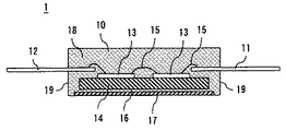
図1はこの発明の実施の形態1における半導体装置の要部を示す斜視図、図2は同装置を構成する半導体モジュールの断面図、図3は同装置の一部を拡大して示す断面図、図4は同装置の半導体モジュールに設けた防液壁の作用説明図である。
1 is a perspective view showing a main part of a semiconductor device according to
この実施の形態1の半導体装置は、半導体モジュール1と液冷部材2とを備える。半導体モジュール1は、直方体状の本体部10の側面19の一方側から電源用の電極端子11が、他方側からスイッチング制御のための制御信号用の電極端子12がそれぞれ外方に引き出されている。
The semiconductor device according to the first embodiment includes a
また、本体部10の内部には半導体素子としてIGBT等の複数個の電力用のスイッチング素子13が銅板等からなるヒートスプレッダ14に半田付け等により固着されており、また、各スイッチング素子13相互間や電極端子11,12との間はアルミ線等の金属細線15によりワイヤボンドされて電気的に接続されている。さらに、ヒートスプレッダ14の裏面側には絶縁層16を介して熱伝導性が良好でかつ腐食しにくい銅等の材料でできたモジュールベース17が配置されている。そして、スイッチング素子13や金属細線15を外環境から保護するため、モジュールベース17から熱を外部に放出する底面を除く全体が封止樹脂18によりモールドされている。なお、モジュールベース17は、スイッチング素子13からの発熱を効率良く外部に伝達するとともに、後述のシール部材3を確実にシールするための役目を同時に果たしている。
In addition, a plurality of
一方、液冷部材2は、銅やアルミニュウムなどの金属やPPS(ポリフェニレンサルファイド)等の樹脂からなるもので、その内部には冷却液の流通路20が形成されるとともに、その流通路20の一部が外部に露出するように削除されて開口部21が設けられている。また、この開口部21の周縁部分にはOリング等のシール部材3を装着する装着溝22が形成されている。
On the other hand, the
そして、半導体モジュール1の冷却面となるモジュールベース17が液冷部材2の流通路20の開口部21に臨むように、装着溝22内にシール部材3を装着した状態で半導体モジュール1と液冷部材2とを位置合わせして両者1,2を図示しないボルト等によって締結される。そして、液冷部材2の流通路20にエチレングリコール等の粘性の高い液体の水溶液などからなる冷却液を流すことで、半導体モジュール1を構成するスイッチング素子13がモジュールベース17等を介して冷却液によって直接冷却されるとともに、流通路20から冷却液が外部に漏れないようシール部材3によってにシールされる。
Then, the
さらに、この実施の形態1の特徴として、半導体モジュール1の本体部10には、電極端子11,12の突出側において各電極端子11,12とシール部材3との間に位置する箇所に防液壁4が一体的に設けられている。
Further, as a feature of the first embodiment, the
すなわち、この防液壁4は、その一端部41側が半導体モジュール1の本体部10底面のシール部材3よりも外側の位置に接着剤などで固定され、また、他端部42側は本体部10の電極端子11,12の突出側の側面19に沿う状態から電極端子11,12に沿って外方に向けて張り出した状態となるように順次屈曲されて鉤形に形成されている。そして、この防液壁4の他端部42の先端は、液冷部材2の側面23よりも僅かに外方に突出している。なお、防液壁4の材質としては、電極端子11,12の絶縁耐圧を考慮すると、合成樹脂やセラミック等の絶縁材料が好適に使用される。
That is, the
上記構成において、半導体モジュール1と液冷部材2とを図示しないボルト等によって締結する際のシール部材3に対する加圧力の不均一や、半導体モジュール1と液冷部材2との接合面への異物の噛み込み、あるいはシール部材3の傷や経年劣化等に起因して、冷却液Lがシール部材3の外部に漏出した場合、この漏液Lは液冷部材2の上に広がってその側面23まで流れ出すものの、半導体モジュール1の本体部10に防液壁4が設けられているために、その上方の電極端子11,12を濡らすことはない。したがって、装置を立てた状態で設置した場合でも、電極端子11,12同士が漏液Lによって電気的に短絡するといった不具合発生を確実に防止することができる。
In the above configuration, the pressure applied to the
また、液冷部材2には従来技術のように漏液排出溝や液抜き穴を形成する必要がなく、漏液排出溝を半導体モジュール1の底部で閉鎖して管状にする必要もないため、装置全体の形状を小型化することができる。さらに、漏液排出溝や液抜き穴の形成するための切削加工が不要で、半導体モジュール1の本体部10に防液壁4の形成部材を固定するだけで済むため、比較的安価に実現することが可能となる。
Further, the
なお、この実施の形態1において、防液壁4は鉤形に形成されているが、このような形状に限らず、例えば、本体部10底面のシール部材3よりも外側の位置から電極端子11,12に沿って平行に張り出した平板状のものであってもよい。また、この実施の形態1において、防液壁4は本体部10の電極端子11,12の突出側にだけ設けているが、本体部10の周囲にわたって連続的に形成することも可能である。この構成にすれば、漏液が防液壁4が無い部分から電極端子11,22側に回り込むのが阻止できるので、電極端子11,12間の短絡発生を一層確実に防止することができる。
In the first embodiment, the
実施の形態2.
図5はこの発明の実施の形態2における半導体装置の構成を示す断面図であり、図1ないし図4に示した実施の形態1と同一または相当する構成部分に同一の符号を付す。
FIG. 5 is a cross-sectional view showing the configuration of the semiconductor device according to the second embodiment of the present invention, and the same reference numerals are given to the same or corresponding components as those of the first embodiment shown in FIGS.
この実施の形態2の特徴は、防液壁4の一端部41側が半導体モジュール1の本体部10の底面に固定されるのではなく、本体部10の底面と略直交する側面19に接着剤によって直接に固定されていることである。
The feature of the second embodiment is that the one
この実施の形態2のように、半導体モジュール1の本体部10の側面19に防液壁4を直接固定した構成とした場合には、本体部10の底面に防液壁4を固定するための接着スペースを確保する必要がないので、半導体モジュール1を液冷部材2にボルト等によって締結する場合のシール部材3に対する締め付け力を加減する際の自由度が高くなるとともに、防液壁4の取り付け作業も容易になり、加工性が改善される。
その他の構成、および作用効果は実施の形態1の場合と同様であるから、ここでは詳しい説明は省略する。
When the liquid-
Since other configurations and operational effects are the same as those in the first embodiment, detailed description thereof is omitted here.
実施の形態3.
図6はこの発明の実施の形態3における半導体装置の構成を示す断面図であり、図1ないし図4に示した実施の形態1と同一または相当する構成部分に同一の符号を付す。
FIG. 6 is a cross-sectional view showing the configuration of the semiconductor device according to the third embodiment of the present invention, and the same reference numerals are given to the same or corresponding components as those of the first embodiment shown in FIGS.
この実施の形態3の特徴は、防液壁4の張り出し側の先端部に液冷部材2に向けて屈曲された防液土手43が形成されていることである。
A feature of the third embodiment is that a liquid-
このような防液土手43を設けることにより、例えば漏液Lが特に多い場合や、装置が傾斜したり立てた状態で設置された場合に、漏液Lが防液壁4の先端まで達しても、防液土手43によってせき止められるため、漏液が電極端子11,12まで回り込んでくるのを確実に阻止することができ、電極端子11,12同士が漏液によって電気的に短絡するといった不具合発生を実施の形態1の場合よりもさらに一層確実に防止することができる。
その他の構成、および作用効果は実施の形態1の場合と同様であるから、ここでは詳しい説明は省略する。
By providing such a liquid-
Since other configurations and operational effects are the same as those in the first embodiment, detailed description thereof is omitted here.
実施の形態4.
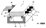
図7はこの発明の実施の形態4における半導体装置の要部を示す斜視図、図8は同装置の正面断面図、図9は同装置の側面断面図であり、図1ないし図4に示した実施の形態1と同一または相当する構成部分に同一の符号を付す。
7 is a perspective view showing a main part of a semiconductor device according to
この実施の形態4の特徴は、半導体モジュール1の本体部10に設けられた防液壁4の内、電源用の電極端子11に対して設けられた防液壁4については、電極端子11の突出方向と直交する側方を囲むように、互いに隣接する電極端子11の間に側壁部44が個別に立設されている。また、制御信号用の電極端子12に対して設けられた防液壁4については、電極端子12の突出方向と直交する配列方向の左右両端を囲むように側壁部44が形成されている。
The feature of the fourth embodiment is that the
このように、防液壁4に側壁部44を一体的に設けることより、例えば漏液が特に多い場合や、装置が傾斜したり立てた状態で設置された場合でも、側壁部44によって漏液が防液壁4の側面から電極端子11,12側に回り込んでくるのを確実に阻止することができ、電極端子11,12同士が漏液によって電気的に短絡するといった不具合発生を一層確実に防止することができる。さらに、電源用の電極端子11の相互間に側壁部44が介在することにより当該電極端子11間の空間絶縁距離を長くすることができて絶縁性を高めることができるという付随的な効果も得られる。
Thus, by providing the
なお、この実施の形態4では、制御信号用の電極端子12に対して設けられた防液壁4については、電極端子12の配列方向の左右両端の2箇所にのみ側壁部44を設けているが、電源用の電極端子11の場合と同様に、互いに隣接する電極端子12の間に側壁部44を個別に立設した構成とすることも可能である。また、逆に、電源用の電極端子11に対して個別に側壁部44を形成する代わりに、電極端子12の配列方向の左右両端の2箇所に側壁部44を形成してもよい。
その他の構成、および作用効果は実施の形態1の場合と同様であるから、ここでは詳しい説明は省略する。
In the fourth embodiment, with respect to the
Since other configurations and operational effects are the same as those in the first embodiment, detailed description thereof is omitted here.
実施の形態5.
この発明の実施の形態5における特徴は、前述の各実施の形態1〜4において、防液壁4の表面(実施の形態3,4では防液土手43や側壁部44の表面も含む)に撥水処理が施される一方、液冷部材2の防液壁4に対向する表面に親水性処理が施されていることである。
Embodiment 5 FIG.
A feature of the fifth embodiment of the present invention is that in each of the first to fourth embodiments described above, the surface of the liquid-proof wall 4 (including the surfaces of the liquid-
この場合の撥水処理は、例えば、防液壁4の表面にワックス類やフッ素樹脂等の撥水性のコーティング材を塗布することによって実現することができる。また、親水性処理は、例えば、液冷部材2の所定の表面に酸化チタン粉末等の親水性のコーティング材を塗布することによって実現することができる。
The water repellent treatment in this case can be realized by, for example, applying a water repellent coating material such as waxes or fluororesin to the surface of the
ここで、液冷部材2の流通路20内を流れる冷却液としては、例えばエチレングリコール等の比較的粘性の高い液体の水溶液が用いられることから、防液壁4の表面に撥水処理を施すことにより、漏液が防液壁4の表面に濡れ広がるのを阻止できる一方、液冷部材2の防液壁4に対向する表面に親水性処理を施すことにより、漏液が液冷部材2表面へ濡れ広がるのを促進させることができる。このため、漏液が防液壁4を超えて濡れ広がって電極端子11,12を短絡させるのを防止することができる。
Here, as the coolant flowing in the
なお、この実施の形態5のように、防液壁4の表面への撥水処理と液冷部材2の表面への親水性処理の双方を施すことが好ましいが、必要に応じて防液壁4の表面への撥水処理と液冷部材2の防液壁4に対向する表面への親水性処理とのいずれか一方の処理のみを施すことも可能である。
In addition, it is preferable to perform both the water-repellent treatment on the surface of the liquid-
この発明は、上記の実施の形態1〜5の各個別の構成に限定されるものではなく、実施の形態1〜5の構成を適宜組み合わせることができるのは勿論である。 The present invention is not limited to the individual configurations of the first to fifth embodiments, and it is needless to say that the configurations of the first to fifth embodiments can be appropriately combined.
また、上記の実施の形態1〜5では、半導体モジュール1の本体部10の対向する両側面19から電極端子11,12が突出形成された構成の場合について説明したが、この発明はこのような構成に限らず、例えば、従来のように電極端子が本体部の上部から突出した構成のものにも適用することができ、同様の効果が得られる。
Moreover, in said Embodiment 1-5, although the case where the
さらに、上記の実施の形態1〜5では、半導体モジュール1を構成する半導体素子として電力用のIGBT等の電力用のスイッチング素子13を備えた場合について説明したが、この発明はこのようなものに限らず、高集積で高速の論理素子の複数個をパッケージ化した半導体モジュール1を備えた半導体装置に対しても、同様に適用することが可能である。
Further, in the above first to fifth embodiments, the case where the
1 半導体モジュール、10 本体部、11 電源側の電極端子、
12 制御信号側の電極端子、13 スイッチング素子(半導体素子)、19 側面、
2 液冷部材、20 流通路、21 開口部、3 シール部材、4 防液壁、
43 防液土手、44 側壁部。
DESCRIPTION OF
12 control signal side electrode terminal, 13 switching element (semiconductor element), 19 side surface,
2 liquid cooling members, 20 flow passages, 21 openings, 3 seal members, 4 liquid barriers,
43 Liquidproof bank, 44 Side wall.
Claims (6)
上記半導体モジュールには、その電極端子と上記シール部材との間に位置し、かつ、上記液冷部材との接合面と略直交する側面の外方に向けて張り出した防液壁が一体的に設けられていることを特徴とする半導体装置。 A semiconductor module on which a semiconductor element is mounted; and a liquid cooling member having a cooling liquid flow passage therein and having an opening formed so that a part of the flow passage is exposed to the outside. In the direct liquid cooling type semiconductor device in which the module and the liquid cooling member are integrally joined via a sealing member, and the cooling surface of the semiconductor module faces the opening of the flow path,
The semiconductor module is integrally provided with a liquid barrier wall that is located between the electrode terminal and the seal member and projects outwardly from the side surface substantially orthogonal to the joint surface with the liquid cooling member. A semiconductor device provided.
Priority Applications (1)
| Application Number | Priority Date | Filing Date | Title |
|---|---|---|---|
| JP2006018650A JP2007201224A (en) | 2006-01-27 | 2006-01-27 | Semiconductor device |
Applications Claiming Priority (1)
| Application Number | Priority Date | Filing Date | Title |
|---|---|---|---|
| JP2006018650A JP2007201224A (en) | 2006-01-27 | 2006-01-27 | Semiconductor device |
Publications (1)
| Publication Number | Publication Date |
|---|---|
| JP2007201224A true JP2007201224A (en) | 2007-08-09 |
Family
ID=38455492
Family Applications (1)
| Application Number | Title | Priority Date | Filing Date |
|---|---|---|---|
| JP2006018650A Pending JP2007201224A (en) | 2006-01-27 | 2006-01-27 | Semiconductor device |
Country Status (1)
| Country | Link |
|---|---|
| JP (1) | JP2007201224A (en) |
Cited By (2)
| Publication number | Priority date | Publication date | Assignee | Title |
|---|---|---|---|---|
| JP2015213143A (en) * | 2014-04-15 | 2015-11-26 | トヨタ自動車株式会社 | Power converter and manufacturing method thereof |
| JP2016111250A (en) * | 2014-12-09 | 2016-06-20 | トヨタ自動車株式会社 | On-vehicle electronic apparatus |
-
2006
- 2006-01-27 JP JP2006018650A patent/JP2007201224A/en active Pending
Cited By (2)
| Publication number | Priority date | Publication date | Assignee | Title |
|---|---|---|---|---|
| JP2015213143A (en) * | 2014-04-15 | 2015-11-26 | トヨタ自動車株式会社 | Power converter and manufacturing method thereof |
| JP2016111250A (en) * | 2014-12-09 | 2016-06-20 | トヨタ自動車株式会社 | On-vehicle electronic apparatus |
Similar Documents
| Publication | Publication Date | Title |
|---|---|---|
| JP5382049B2 (en) | Semiconductor device | |
| US8699225B2 (en) | Liquid cooled electronics assembly suitable to use electrically conductive coolant | |
| US7242582B2 (en) | Semiconductor module mounting structure, a cardlike semiconductor module, and heat receiving members bonded to the cardlike semiconductor module | |
| CN106098631B (en) | Package for semiconductor device | |
| JP5206822B2 (en) | Semiconductor device | |
| CN111066116B (en) | power conversion device | |
| JP6503909B2 (en) | Semiconductor device | |
| US9131630B2 (en) | Edge seal for electronics assembly suitable for exposure to electrically conductive coolant | |
| CN102187456A (en) | Semiconductor device cooling structure and power converter provided with the cooling structure | |
| US20140367842A1 (en) | Power semiconductor device and method of manufacturing the same | |
| JP2022087498A (en) | Cooler and semiconductor device | |
| JP2004128099A (en) | Water cooling inverter | |
| CN103947095A (en) | Power converter | |
| JP2019125700A (en) | Power semiconductor device | |
| JP2005032904A (en) | Direct liquid-cooled power semiconductor module | |
| JP2000068447A (en) | Power module | |
| JPWO2015194023A1 (en) | Power module device and power conversion device | |
| JP2004259791A (en) | Power semiconductor module | |
| JP2007201224A (en) | Semiconductor device | |
| JP2004253495A (en) | Liquid-cooled power semiconductor module and inverter including the same | |
| JP4120581B2 (en) | Power module | |
| JP2007201225A (en) | Semiconductor device | |
| JP2004096135A5 (en) | ||
| CN114203650A (en) | Semiconductor device and method for manufacturing semiconductor device | |
| JP2005019849A (en) | Semiconductor cooling device |