JP2007201380A - Air turn roller device - Google Patents
Air turn roller device Download PDFInfo
- Publication number
- JP2007201380A JP2007201380A JP2006021207A JP2006021207A JP2007201380A JP 2007201380 A JP2007201380 A JP 2007201380A JP 2006021207 A JP2006021207 A JP 2006021207A JP 2006021207 A JP2006021207 A JP 2006021207A JP 2007201380 A JP2007201380 A JP 2007201380A
- Authority
- JP
- Japan
- Prior art keywords
- semiconductor device
- air
- tape
- rotating roller
- roller
- Prior art date
- Legal status (The legal status is an assumption and is not a legal conclusion. Google has not performed a legal analysis and makes no representation as to the accuracy of the status listed.)
- Granted
Links
Images



Landscapes
- Advancing Webs (AREA)
- Registering, Tensioning, Guiding Webs, And Rollers Therefor (AREA)
- Wire Bonding (AREA)
Abstract
【課題】半導体装置用テープにおける配線パターン部分に中折れを生じさせたり損傷を与えることなく搬送可能にしたエアーターンローラー装置を提供する。
【解決手段】回転ローラー56の外周ガイド面部62に、半導体装置用テープ16の幅方向両端部にそれぞれ転接する転接段部66、68、70を形成し、これら転接段部70の間に一段低い外周面である逃げ凹部72を形成し、逃げ凹部72の部分に送気口74を穿設し、回転ローラー56の両側面部分から空気が漏れることを抑制する半密閉手段を設け、送気ファン82で回転ローラー56の空洞内部に空気を送気し送気口74から噴射させ半導体装置用テープ16の幅方向中間部に空気を吹き付けて逃げ凹部72から浮き上がらせた状態で回転ローラー56が回転して半導体装置用テープ16が搬送される。
【選択図】図1The present invention provides an air turn roller device which can be conveyed without causing bending or damage to a wiring pattern portion in a tape for a semiconductor device.
Rolling contact step portions 66, 68, and 70 are formed on the outer peripheral guide surface portion 62 of the rotating roller 56 so as to make rolling contact with both end portions in the width direction of the tape 16 for a semiconductor device, respectively. A relief recess 72, which is a lower outer peripheral surface, is formed, an air supply port 74 is formed in the relief recess 72, and a semi-sealing means for suppressing air leakage from both side portions of the rotary roller 56 is provided. In the state where air is blown into the cavity of the rotating roller 56 by the air fan 82 and sprayed from the air supply port 74, the air is blown to the intermediate portion in the width direction of the tape 16 for semiconductor device and lifted from the escape recess 72. Rotates and the semiconductor device tape 16 is conveyed.
[Selection] Figure 1
Description
この発明は、半導体チップを搭載するTAB(Tape Automated Bonding)テープ等の半導体装置用テープを検査するために搬送するのに用いて好適なエアーターンローラー装置に関する。 The present invention relates to an air turn roller device suitable for use in transporting a semiconductor device tape such as a TAB (Tape Automated Bonding) tape on which a semiconductor chip is mounted.
一般に、半導体装置の小型化の要求が強まっており、そのため、半導体装置の外形寸法をほぼ半導体素子の外形寸法にまで小型化したチップサイズパッケージ(以後、CSPと称す。)の半導体装置が用いられている。 Generally, there is an increasing demand for downsizing of a semiconductor device. For this reason, a semiconductor device of a chip size package (hereinafter referred to as CSP) in which the outer dimensions of the semiconductor device are reduced to almost the outer dimensions of a semiconductor element is used. ing.
このCSPの半導体装置では、基板の材料となる半導体装置用テープ上に半導体素子を接着剤などで固着し、半導体素子の周縁部に形成された電極と基板の周縁部に形成された電極とを金線等のワイヤボンディングで電気的に接続した構成のものや、半導体装置用テープ上に形成したアレイ状の電極と半導体素子の裏面側にアレイ状に形成された半田ボールとを、半田ろう付けして電気的に接続する構成のものといった様々な構成のCSPの半導体装置が提案されている。 In this CSP semiconductor device, a semiconductor element is fixed on a semiconductor device tape, which is a material of the substrate, with an adhesive or the like, and an electrode formed on the peripheral portion of the semiconductor element and an electrode formed on the peripheral portion of the substrate are provided. Solder brazing of electrodes connected by wire bonding such as gold wires, or arrayed electrodes formed on a tape for semiconductor devices and solder balls formed in an array on the back side of the semiconductor element There have been proposed CSP semiconductor devices having various configurations such as an electrical connection configuration.
また、半導体装置の製造においては、長尺に形成された半導体装置用テープに、1チップに対応して配線、電極、ビームリード及びスルーホール等の配線パターンを複数繰り返してパタンニングし、各チップに対応して半導体素子を実装してから、チップ毎に切断し、一度に大量の半導体装置を製造する方法が提案されている。 Further, in the manufacture of semiconductor devices, a plurality of wiring patterns such as wiring, electrodes, beam leads, and through holes are repeatedly patterned on a long semiconductor device tape corresponding to one chip. A method of manufacturing a large number of semiconductor devices at one time by mounting a semiconductor element corresponding to the above, and then cutting each chip is proposed.
このように用いられる半導体装置用テープは、ポリイミド基材等の可撓性を有する長尺のシート状基材の表面に形成された銅の導電膜を、エッチング技術又はプレス加工等により、各チップに対応した所定の配線、電極、ビームリード及びスルーホール等の配線パターンを複数繰り返して構成する。 The tape for a semiconductor device used in this way is obtained by etching a copper conductive film formed on the surface of a long sheet-like base material having flexibility such as a polyimide base material by an etching technique or pressing. A plurality of wiring patterns such as predetermined wiring, electrodes, beam leads, and through holes corresponding to the above are repeated.
また、この半導体装置用テープには、その各チップに対応した配線パターンの範囲外となる長手方向両端部に、それぞれ送り操作をする送り爪を挿入するための小矩形透穴を所定間隔で一列に穿設する。 In addition, in this tape for a semiconductor device, small rectangular through holes for inserting feeding claws for feeding operations are arranged at predetermined intervals at both ends in the longitudinal direction that are outside the range of the wiring pattern corresponding to each chip. Drill into.
この半導体装置用テープには、その幅を35mm、48mm、70mm或いは96mm等の各所定サイズに形成したものがある。 Some of these tapes for semiconductor devices are formed in a predetermined size such as 35 mm, 48 mm, 70 mm or 96 mm.
また、このように構成される半導体装置用テープは、そのパターン形成後に配線に断線や欠け等のパターン欠陥を検査装置で検査してから半導体装置の製造に用いられる。 Further, the semiconductor device tape configured as described above is used for manufacturing a semiconductor device after a pattern is formed and a pattern defect such as disconnection or chipping is inspected with an inspection device.
この検査装置では、半導体装置用テープ表面の配線パターンをCCD等の画像読取装置により画像データとして読み取り、この読み取られた画像データに基づいてパターン幅や配線パターンの断線、ショートなどの欠陥を検出する検査を行う。 In this inspection apparatus, a wiring pattern on the surface of a semiconductor device tape is read as image data by an image reading device such as a CCD, and a defect such as a pattern width, a disconnection of a wiring pattern, or a short circuit is detected based on the read image data. Perform an inspection.
この検査装置は、半導体装置用テープを引き出す巻き出しユニットと半導体装置用テープを巻き取る巻き取りユニットとの間に、複数の搬送用のローラーを用いた搬送手段で搬送路を構成し、この搬送路上に、画像読取装置を備えたスキャナーユニット、不良部分に対応してマーキングを施すマーキングユニット等を順に配置して構成する(例えば、特許文献1参照)。 In this inspection apparatus, a transport path is formed by a transport means using a plurality of transport rollers between a winding unit for pulling out a semiconductor device tape and a winding unit for winding the semiconductor device tape. A scanner unit including an image reading device, a marking unit for marking corresponding to a defective portion, and the like are sequentially arranged on the road (for example, see Patent Document 1).
また、この検査装置では、半導体装置用テープの表面に形成された配線パターンに搬送用のローラーの外周面が当接して損傷を与えることを防止することが要求される。 Further, in this inspection apparatus, it is required to prevent the outer peripheral surface of the transfer roller from coming into contact with the wiring pattern formed on the surface of the semiconductor device tape to cause damage.
このため、この検査装置では、搬送用のローラーを、その外周面における幅方向両側にそれぞれ配線パターンの範囲外となる長手方向両端部の小矩形透穴の列を設けた部分だけを当接させる転接面部を形成し、搬送用のローラー外周面における幅方向両側の転接面部の間部分に一段低い逃げ凹部を形成したいわゆる段付きローラーに構成することが考えられる。 For this reason, in this inspection apparatus, the conveyance roller is brought into contact only with the portion provided with the rows of small rectangular through holes at both ends in the longitudinal direction that are outside the range of the wiring pattern on both sides in the width direction on the outer peripheral surface thereof. It is conceivable to form a so-called stepped roller in which a rolling contact surface portion is formed and a relief recess that is one step lower is formed in a portion between the rolling contact surface portions on both sides in the width direction on the outer peripheral surface of the conveying roller.
このように構成した段付きローラーを用いて、長尺で可撓性の帯状シート部材である半導体装置用テープを搬送する場合には、搬送用のローラーに半導体装置用テープを巻回した状態で、半導体装置用テープの長手方向両端部の小矩形透穴の列を設けた部分だけが搬送用のローラー外周の転接面部に転接し半導体装置用テープの配線パターン部分が中に浮いた状態として搬送用のローラーの外周面と非接触の状態で搬送できるので配線パターン部分に傷が付くことを防止することができる。 When transporting a tape for a semiconductor device, which is a long and flexible strip-shaped sheet member, using the stepped roller configured as described above, the semiconductor device tape is wound around a transport roller. Only the portion provided with the rows of small rectangular through holes at both ends in the longitudinal direction of the tape for the semiconductor device is in contact with the rolling contact surface portion of the outer periphery of the transport roller, and the wiring pattern portion of the tape for the semiconductor device is floated inside Since it can convey in the state which is not in contact with the outer peripheral surface of the roller for conveyance, it can prevent that a wiring pattern part is damaged.
しかし、検査装置において、段付きローラーを用いて半導体装置用テープを搬送する場合には、半導体装置用テープが薄くなると、半導体装置用テープの幅方向中央部が一段低い逃げ凹部側に折れ曲がって入り込み配線パターン部分に皺を作るいわゆる中折れを生じることがあるという問題がある。
本発明は、上述した点に鑑み、半導体装置用テープにおける配線パターン部分に中折れを生じさせたり損傷を与えることなく、半導体装置用テープを搬送可能に構成したエアーターンローラー装置を新たに提供することを目的とする。 In view of the above, the present invention newly provides an air turn roller device configured to be capable of transporting a semiconductor device tape without causing breakage or damage to a wiring pattern portion in the semiconductor device tape. For the purpose.
本発明の請求項1に記載のエアーターンローラー装置は、長尺帯状の半導体装置用テープを回転ローラーの所定範囲に巻き掛けた状態で回転することにより、半導体装置用テープを搬送するのに用いるエアーターンローラー装置において、回転ローラーの外周ガイド面部に、半導体装置用テープの幅方向両端部にそれぞれ転接するよう段状に形成した転接段部と、回転ローラーの外周ガイド面部の幅方向中間部に、一段低い外周面として形成された逃げ凹部と、回転ローラーの逃げ凹部の部分に、穿設された送気口と、回転ローラーの側面部分から空気が漏れることを抑制して回転ローラーの内部に空洞を作るように配置される半密閉手段と、回転ローラーの空洞内部に空気を送気して送気口から噴射させることにより長手方向両側部を各転接段部に転接させている半導体装置用テープの幅方向中間部に向けて空気を吹き付けて、半導体装置用テープを逃げ凹部から浮き上がらせるための送気ファンと、を有することを特徴とする。 The air turn roller device according to claim 1 of the present invention is used to transport a tape for a semiconductor device by rotating the tape for a semiconductor device in a long band around a predetermined range of a rotating roller. In an air turn roller device, a rolling step formed in a step shape so as to be in rolling contact with both ends of the tape for a semiconductor device on the outer peripheral guide surface of the rotating roller, and an intermediate portion in the width direction of the outer peripheral guide surface of the rotating roller In addition, the escape recess formed as a lower outer peripheral surface, the air supply port formed in the relief recess portion of the rotating roller, and the inside of the rotating roller by suppressing air leakage from the side surface portion of the rotating roller Semi-sealing means arranged so as to create a cavity, and air is fed into the inside of the cavity of the rotating roller and jetted from the air feeding port to rotate each side of the longitudinal direction. By blowing air toward the width direction intermediate portion of the tape for semiconductor devices by rolling contact with the step portion, and having a a air blower for float from the recess flank of the tape for semiconductor devices.
本発明の請求項2に記載のエアーターンローラー装置は、長尺帯状の半導体装置用テープを回転ローラーの所定範囲に巻き掛けた状態で回転することにより、半導体装置用テープを搬送するのに用いるエアーターンローラー装置において、回転ローラーの外周ガイド面部に、半導体装置用テープの幅方向両端部にそれぞれ転接するよう段状に形成した転接段部と、回転ローラーの外周ガイド面部の幅方向中間部に、一段低い外周面として形成された逃げ凹部と、回転ローラーの逃げ凹部の部分に、穿設された送気口と、回転ローラーの一方の側面を部分から空気が漏れることを抑制するように塞ぐ端面板と、回転ローラーの他方の側面部分から空気が漏れることを抑制して回転ローラーの内部に空洞を作るように配置した支持端面部材及び取り付け端面部材と、取り付け端面部材に取り付けられ、回転ローラーの空洞内部に空気を送気して送気口から噴射させることにより長手方向両側部を各転接段部に転接させている半導体装置用テープの幅方向中間部に向けて空気を吹き付けて、半導体装置用テープを逃げ凹部から浮き上がらせるための送気ファンと、を有することを特徴とする。 The air turn roller device according to claim 2 of the present invention is used to convey a tape for a semiconductor device by rotating the tape for a semiconductor device in a long band around a predetermined range of a rotating roller. In an air turn roller device, a rolling step formed in a step shape so as to be in rolling contact with both ends of the tape for a semiconductor device on the outer peripheral guide surface of the rotating roller, and an intermediate portion in the width direction of the outer peripheral guide surface of the rotating roller In addition, the escape recess formed as a lower outer peripheral surface, the air supply port formed in the escape recess portion of the rotating roller, and one side surface of the rotating roller to suppress air leakage from the portion The end face plate to be closed, the support end face member disposed so as to prevent the air from leaking from the other side surface portion of the rotating roller, and to form a cavity inside the rotating roller A semiconductor device attached to the attachment end face member and the attachment end face member, in which air is supplied into the cavity of the rotating roller and jetted from the air supply port so that both sides in the longitudinal direction are brought into rolling contact with each rolling contact step portion. And an air supply fan for blowing air toward the intermediate portion in the width direction of the tape for use in the semiconductor device so as to lift the tape for the semiconductor device from the recessed portion.
本発明の請求項3に記載のエアーターンローラー装置は、長尺帯状の半導体装置用テープを回転ローラーの所定範囲に巻き掛けた状態で回転することにより、半導体装置用テープを搬送するのに用いるエアーターンローラー装置において、回転ローラーの外周ガイド面部に、半導体装置用テープの幅方向両端部にそれぞれ転接するよう段状に形成した転接段部と、回転ローラーの外周ガイド面部の幅方向中間部に、一段低い外周面として形成された逃げ凹部と、回転ローラーの逃げ凹部の部分に、穿設された送気口と、回転ローラーの一方の側面を部分から空気が漏れることを抑制するように塞ぐ端面板と、回転ローラーの他方の側面部分から空気が漏れることを抑制して回転ローラーの内部に空洞を作るように配置した閉塞用の支持端面部材と、回転ローラーの外周における半導体装置用テープを巻回しない所定範囲に配置したエアガイド部材と、エアガイド部材の外側に取り付けられ、回転ローラーの空洞内部に空気を送気して送気口から噴射させることにより長手方向両側部を各転接段部に転接させている半導体装置用テープの幅方向中間部に向けて空気を吹き付けて、半導体装置用テープを逃げ凹部から浮き上がらせるための送気ファンと、を有することを特徴とする。 The air turn roller device according to claim 3 of the present invention is used for transporting a tape for a semiconductor device by rotating the tape for a semiconductor device in a long band around a predetermined range of a rotating roller. In an air turn roller device, a rolling step formed in a step shape so as to be in rolling contact with both ends of the tape for a semiconductor device on the outer peripheral guide surface of the rotating roller, and an intermediate portion in the width direction of the outer peripheral guide surface of the rotating roller In addition, the escape recess formed as a lower outer peripheral surface, the air supply port formed in the escape recess portion of the rotating roller, and one side surface of the rotating roller to suppress air leakage from the portion End face plate for closing and supporting end face part for closing arranged so as to prevent the air from leaking from the other side surface part of the rotating roller and to create a cavity inside the rotating roller. And an air guide member arranged in a predetermined range where the tape for the semiconductor device is not wound around the outer periphery of the rotating roller, and attached to the outside of the air guide member, and air is supplied into the cavity of the rotating roller from the air supply port. Air is blown toward the intermediate portion in the width direction of the tape for semiconductor devices in which both sides in the longitudinal direction are in rolling contact with the respective rolling contact step portions by jetting, so that the semiconductor device tape is lifted from the escape recess. And an air fan.
前述のように構成することにより、送気ファンを駆動し回転ローラーの空洞内部に空気を送気して送気口から噴射させることにより、この回転ローラーに半導体装置用テープの長手方向両側部が各転接段部に転接した状態で巻回されている半導体装置用テープの幅方向中間部に向けて空気を吹き付けて、この半導体装置用テープが逃げ凹部から浮き上がる状態を維持しながら回転ローラーが回転して半導体装置用テープを搬送するので、半導体装置用テープに形成された配線パターン部分に中折れを生じさせたり損傷を与えることなく搬送できる。 By configuring as described above, the air supply fan is driven to supply air into the inside of the cavity of the rotating roller and sprayed from the air supply port, so that both sides in the longitudinal direction of the tape for the semiconductor device are formed on the rotating roller. Rotating rollers while blowing air toward the intermediate portion in the width direction of the tape for a semiconductor device wound in a state of rolling contact with each rolling contact step, and maintaining the state where the tape for a semiconductor device is lifted from the recess Rotates and conveys the semiconductor device tape, so that it can be conveyed without causing the wiring pattern portion formed on the semiconductor device tape to be bent or damaged.
本発明のエアーターンローラー装置によれば、半導体装置用テープにおける配線パターン部分に中折れを生じさせたり損傷を与えることなく、半導体装置用テープを搬送できるという効果がある。 According to the air turn roller device of the present invention, there is an effect that the semiconductor device tape can be transported without causing the wiring pattern portion in the semiconductor device tape to bend or damage.
以下、本発明のエアーターンローラー装置に関する第1実施の形態について、図1乃至図4を参照しながら説明する。 Hereinafter, a first embodiment relating to an air turn roller device of the present invention will be described with reference to FIGS. 1 to 4.
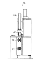
図1及び図2は、本第1実施の形態に係るエアーターンローラー装置を備えた半導体装置用テープの欠陥を検査するための検査装置の全体概略正面図と、全体概略側面図であり、図で10は、検査装置の本体である。 1 and 2 are an overall schematic front view and an overall schematic side view of an inspection apparatus for inspecting a defect of a tape for a semiconductor device provided with an air turn roller device according to the first embodiment. 10 is the main body of the inspection apparatus.
この検査装置10の前面には、検査対象である長尺帯状の半導体装置用テープ16を供給するための巻き出しユニット12と、検査済みの半導体装置用テープ16を回収するための巻き取りユニット14とを配置する。
On the front surface of the
この巻き出しユニット12は、予め多数のパッケージパターンが繰り返し形成された半導体装置用テープ16を巻装したテープリール20を回動可能に保持する巻き出し側リール軸22を備える。
The
また、巻き取りユニット14は、検査済みの半導体装置用テープ16を巻き取るテープリール24を回転駆動可能に装填する巻き取り側リール軸18を備える。
The take-
この検査装置10の前面には、巻き出しユニット12から巻き取りユニット14へかけて半導体装置用テープ16を搬送するための搬送路を構成するため、巻き出しユニット12から引き出した半導体装置用テープ16の搬送方向を変更するガイド26、供給側でテープテンションを調整するショートダンサー28、スキャナーユニット用の第1の送りローラー30及び第2の送りローラー32、搬送路途中でテープテンションを調整するロングダンサー34、マーキングユニット用の第1のガイドローラー36及び第2のガイドローラー38、巻き取り側でテープテンションを調整するショートダンサー40、半導体装置用テープ16の搬送方向を変更するガイド42を順に配置する。
On the front surface of the
この検査装置10では、スキャナーユニットを構成するため、第1の送りローラー30と第2の送りローラー32とを所定間隔を開けて水平に配置し、第1の送りローラー30と第2の送りローラー32との間に浮上ステージ44を配置する。
In this
そして、このスキャナーユニットでは、半導体装置用テープ16が第1の送りローラー30から所定高さ上側に位置する浮上ステージ44のガイド面上を通過して第2の送りローラー32へ移行するよう構成する。
The
図示しないが、この浮上ステージ44は、中空構造とし、その内部に圧縮空気を供給してガイド面に形成した細孔から半導体装置用テープ16の裏面に向けて空気を噴出することにより、ガイド面上を半導体装置用テープ16が非接触で移動するよう構成する。
Although not shown, the
この浮上ステージ44のガイド面中央の上方には、フォーカスユニットを備えたカメラユニット46からなる画像読取部を設置する。
Above the center of the guide surface of the
このスキャナーユニットでは、第1の送りローラー30と第2の送りローラー32とを回動することにより半導体装置用テープ16を一方向に一定の速度で搬送しながら、浮上ステージ44上を通過している半導体装置用テープ16上に形成された回路パターンをカメラユニット46で撮影する。
In this scanner unit, the
このスキャナーユニットでは、カメラユニット46で撮影した画像情報を図示しない制御装置に送信して画像処理し、適正なパターンの画像処理情報と比較して配線パターンの欠陥があれば、これを検出する。なお、カメラユニット46で撮影した画像情報等は、モニタ48に表示する。
In this scanner unit, image information captured by the
この検査装置10では、マーキングユニット(この検査装置10ではパンチユニットとする)を構成するため、第1のガイドローラー36と第2のガイドローラー38の間には、欠陥有りと検知されたパッケージパターンの予め定めた位置にパンチ孔を穿孔してマーキングを施すパンチユニット50を設置する。
Since the
上述のように構成した検査装置10では、ロングダンサー34(必要に応じてショートダンサー28及びショートダンサー40も同じ)を、エアーターンローラー装置で構成する。
In the
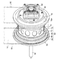
図3に示すように、エアーターンローラー装置としてのロングダンサー34は、固定軸52に対し、ボールベアリング54を介して回転ローラー56を回動自由に装着して構成する。
As shown in FIG. 3, the
この回転ローラー56は、そのボールベアリング54に支受された中心軸部58からラジアル方向に延出する複数のリブ60によって半導体装置用テープ16に転接するための外周面を構成する外周ガイド面部62を支持するように一体的に形成する。
The rotating
図3及び図4に示すように、この回転ローラー56は段付きローラーとして構成するもので、外周ガイド面部62の幅方向両端にそれぞれフランジ端部64を形成し、それらの内側にそれぞれ第1転接段部66を形成し、各第1転接段部66の内側に一段下がった転接面を構成する第2転接段部68を形成し、さらに各第2転接段部68の内側に一段下がった転接面を構成する第3転接段部70を形成し、2つの第3転接段部70の間に、一段低い外周面である逃げ凹部72を形成する。
As shown in FIGS. 3 and 4, the rotating
さらに、この回転ローラー56には、逃げ凹部72の部分に、直径20mm程度の透孔である送気口74を、等間隔で12個穿設する。なお、送気口74は、逃げ凹部72の部分に溝状の透穴を単数又は複数穿設して構成しても良い。
Further, twelve
この回転ローラー56には、側面部分から空気が漏れることを抑制して内部に空洞を作るための半密閉手段として、回転ローラー56の一方の側面を塞ぐための端面板76を設置する。この端面板76は、回転ローラー56の側面にある円形開口より一回り小さい円板状に形成し、その外周縁が回転ローラー56の内側面近傍に位置して、端面板76の外周縁と回転ローラー56の内側面との間から空気が漏れることを抑制できるように形成する。
The rotating
この端面板76は、その中心部に穿設した透孔を、固定軸52に挿通し固定して配置する。なお、この端面板76は、回転ローラー56における中心軸部58と外周ガイド面部62との間を塞ぐように、回転ローラー56と一体的に構成しても良い。
The
また、この回転ローラー56の他方の側面部分(固定軸52の自由端部側の部分)には、空気が漏れることを抑制して内部に空洞を作るための半密閉手段として、支持端面部材78と取り付け端面部材80とを取り付ける。さらに、この取り付け端面部材80には、送気ファン82を取り付ける。
In addition, a support
この支持端面部材78は、その中央部の円形凹部部分に穿設した透孔に、固定軸52のねじ溝を穿設した先端部を挿通し、ナット84で固定して取り付ける。この支持端面部材78の外周には、筒状のリング部78Aを一体的に形成し、リング部78Aの周縁が回転ローラー56の内側面近傍に位置して、リング部78Aと回転ローラー56の内側面との間から空気が漏れることを抑制できるように構成する。
The support
また、図4及び図5に示すように、支持端面部材78の平面部には、複数の円形透孔である通気穴86を平均的に分散するよう等間隔で穿設する。支持端面部材78の平面部には、取り付け端面部材80を重ねるように配置してねじ88で締結する。この取り付け端面部材80には、その中央部に穿設した開口部分を覆うように、送気ファン82をねじ90で取り付ける。
Further, as shown in FIGS. 4 and 5, a plurality of ventilation holes 86 that are circular through holes are formed at equal intervals in the flat portion of the support
この送気ファン82は、外気を、取り付け端面部材80の開口部分及び支持端面部材78の通気穴86を通して回転ローラー56の内部へ送気する機能を持つ。
The
このように構成したエアーターンローラー装置としてのロングダンサー34は、検査装置10の支持機構に支持されて下方に所定の荷重で降下するよう装着し、半導体装置用テープ16を、テープテンションを一定にして搬送するために用いる。
The
すなわち、このロングダンサー34を装着した検査装置10では、半導体装置用テープ16をロングダンサー34に半周程度巻回した状態で搬送することにより、半導体装置用テープ16の搬送動作によって回転ローラー56が固定軸52の周りに回動しながら、半導体装置用テープ16に加わるテープテンションの変動をロングダンサー34の上下動作で吸収する。
That is, in the
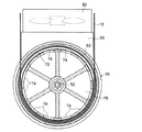
図5に例示するように、このロングダンサー34を利用して搬送される半導体装置用テープ16は、その長手方向両側部にそれぞれ搬送用の爪を引っ掛けるための小矩形透孔92が所定間隔を開けて一列に穿設されている。この半導体装置用テープ16では、小矩形透孔92を穿設した長手方向両側部を後の加工工程で切除して半導体装置を完成させるので、この半導体装置用テープ16の長手方向両側部に回転ローラー56が転接しても半導体装置用テープ表面の配線パターンに損傷を受けることはない。
As illustrated in FIG. 5, the
よって、このロングダンサー34では、半導体装置用テープ16の長手方向両側部だけに転接して半導体装置用テープ16を搬送する。すなわち、このロングダンサー34では、例えば大きな幅サイズの半導体装置用テープ16に対して、その第1転接段部66上に半導体装置用テープ16の長手方向両側部を転接させ若しくは中の幅サイズの半導体装置用テープ16に対して、その第2転接段部68上に半導体装置用テープ16の長手方向両側部を転接させ又は小の幅サイズの半導体装置用テープ16に対して、その第3転接段部70上に半導体装置用テープ16の長手方向両側部を転接させて搬送する。
Therefore, in this
さらに、このロングダンサー34では、送気ファン82で外気を回転ローラー56の内部空洞へ送気して外周ガイド面部62の送気口74から、両側の第1転接段部66若しくは第2転接段部68又は第3転接段部70に長手方向両側部を転接させている半導体装置用テープ16の幅方向中間部に向けて吹き付けることにより、この半導体装置用テープ16の幅方向中間部を逃げ凹部72から所定距離だけ浮き上がらせた状態を維持する。
Further, in this
よって、このロングダンサー34では、その外周ガイド面部62に半周巻回された半導体装置用テープ16の幅方向中間部が送気口74から吹き出す空気に押圧されて半導体装置用テープ16の幅方向中央部が一段低い逃げ凹部72側に折れ曲がって入り込むことがないので、配線パターン部分に皺を作るいわゆる中折れを生じることを防止できる。
Therefore, in this
また、このロングダンサー34では、外周ガイド面部62に半導体装置用テープ16を半周程度巻回して用いるときに、半導体装置用テープ16が巻回されていない範囲にある送気口74から空気が漏れて半導体装置用テープ16に吹き付けるための空気圧が低下することを防止するため、図4に想像線で示すように、外周ガイド面部62の半導体装置用テープ16が巻回されていない範囲に対応してカバー部材94を配置しても良い。
Further, in the
このカバー部材94には、逃げ凹部72の外周面に対応した円弧面94Aを形成する。また、このカバー部材94は、支持枠部材95によってロングダンサー34に取り付ける。
The cover member 94 is formed with an arcuate surface 94 </ b> A corresponding to the outer peripheral surface of the
この支持枠部材95は、逆U字状に形成した枠体の一方の自由端部を固定軸52に固着し、他方の自由端部を取り付け端面部材80に固着して配置する。この支持枠部材95には、外周ガイド面部62の直上位置にカバー部材94を取り付けてカバー部材94の円弧面94Aを逃げ凹部72に隣接させて配置する。このように構成した場合には、回転ローラー56の半導体装置用テープ16が巻回されていない範囲にある送気口74を支持枠部材95で塞ぐようにして空気が漏れることを抑制できる。
The
次に、上述のように構成した検査装置10の作用及び動作を説明する。この検査装置10では、テープリール20から引き出した半導体装置用テープ16を、ガイド26、ショートダンサー28及び第1の送りローラー30により浮上ステージ44のガイド面上を、湾曲した状態で非接触で搬送する。
Next, the operation and operation of the
このとき、浮上ステージ44のガイド面上にある半導体装置用テープ16は、搬送方向に湾曲され、幅方向に一直線状となり、かつカメラユニット46と平行になる。さらに、半導体装置用テープ16は、浮上ステージ44のガイド面からの浮上量が制御されているので、カメラユニット46で適切にピントを合わせて撮影することができる。
At this time, the
このカメラユニット46で撮影された画像情報は、図示しない制御装置へ送信される。制御装置では、送信された画像情報に基づいて画像処理を行ってパターンの欠陥を検出する。
Image information captured by the
制御装置は、欠陥を検出した場合に、パンチユニット50を駆動制御して、欠陥のあるパターンに対応して予め定められた箇所にパンチ孔を穿孔してマーキングを施す。
When the control device detects a defect, the control device drives and controls the
なお、この検査装置10は、ショートダンサー28、ロングダンサー34、ショートダンサー40等をエアーターンローラー装置で構成し、半導体装置用テープ16を非接触でガイドすることにより、搬送時の抵抗を少なくし、薄い半導体装置用テープ16を最適に搬送することができる。
The
次に、本発明のエアーターンローラー装置に関する第2実施の形態について、図6を参照しながら説明する。 Next, 2nd Embodiment regarding the air turn roller apparatus of this invention is described, referring FIG.
本第2実施の形態に係るエアーターンローラー装置では、回転ローラー56の外周における半導体装置用テープ16を巻回しない所定範囲を覆うようにエアガイド部材96を配置し、このエアガイド部材96の外側に送気ファン82を配置して構成する。
In the air turn roller device according to the second embodiment, the
このため、本第2実施の形態に係るエアーターンローラー装置では、回転ローラー56の一方の側面に端面板76を配置して空気漏れを抑制し、他方の側面に閉塞用の支持端面部材78(ここでは、通気穴86を設けていない円板状に形成する)を配置して空気漏れを抑制するように構成する。なお、本第2実施の形態に係るエアーターンローラー装置では、送気ファン82を取り付けるための取り付け端面部材80を省略して構成する。
For this reason, in the air turn roller device according to the second embodiment, the
このエアーターンローラー装置に用いるエアガイド部材96は、外周ガイド面部62における逃げ凹部72の幅程度の幅で、逃げ凹部72の直径以下の長さを持つ矩形筒状に形成し、その逃げ凹部72と対向する開口端縁部(図で下側の開口端縁部)を逃げ凹部72の外周面に沿う円弧状に形成する。
The
このエアガイド部材96の逃げ凹部72と反対側の開口部(図で上側の開口部)には、送気ファン82を一体的に取り付ける。
An
なお、エアガイド部材96を一体的に設けた送気ファン82は、図示しない支持部材等の保持手段で、固定軸52や閉塞用の支持端面部材78等に取り付けて設置する。
The
上述のように構成した本第2実施の形態に係るエアーターンローラー装置では、送気ファン82で吸気した空気をエアガイド部材96でガイドして回転ローラー56の逃げ凹部72にある送気口74を通じて回転ローラー56の空洞内部へ送気する。このように回転ローラー56の空洞内へ強制送気された空気は、回転ローラー56における半導体装置用テープ16が巻回されている範囲に位置する送気口74から噴射して、長手方向両側部を外周ガイド面部62側に転接させている半導体装置用テープ16の幅方向中間部に向けて吹き付けられることにより、この半導体装置用テープ16の幅方向中間部を逃げ凹部72から所定距離だけ浮き上がらせた状態を維持させる。
In the air turn roller device according to the second embodiment configured as described above, the air sucked by the
よって、この本第2実施の形態に係るロングダンサー34では、その外周ガイド面部62に半周巻回された半導体装置用テープ16の幅方向中間部が送気口74から吹き出す空気に押圧されて半導体装置用テープ16の幅方向中央部が一段低い逃げ凹部72側に折れ曲がって入り込むことがないので、配線パターン部分に皺を作るいわゆる中折れを生じることを防止できる。
Therefore, in the
なお、本第2実施の形態における以上説明した以外の構成、作用、及び効果は前述した第1実施の形態と同様であるので、その説明を省略する。 Note that the configurations, operations, and effects of the second embodiment other than those described above are the same as those of the first embodiment described above, and thus description thereof is omitted.
また、本発明は、上述した実施の形態に限定されるものではなく、本発明の要旨を逸脱しない範囲で、その他種々の構成を取り得ることは勿論である。 Further, the present invention is not limited to the above-described embodiment, and it is needless to say that various other configurations can be taken without departing from the gist of the present invention.
10 検査装置
16 半導体装置用テープ
26 ガイド
28 ショートダンサー
30 第1の送りローラー
32 第2の送りローラー
34 ロングダンサー
36 ガイドローラー
38 ガイドローラー
40 ショートダンサー
42 ガイド
56 回転ローラー
62 外周ガイド面部
66 第1転接段部
68 第2転接段部
70 第3転接段部
72 逃げ凹部
74 送気口
76 端面板
78Aリング部
78 支持端面部材
80 取り付け端面部材
82 送気ファン
86 通気穴
94 カバー部材
94A円弧面
95 支持枠部材
96 エアガイド部材
10
Claims (3)
前記回転ローラーの外周ガイド面部に、前記半導体装置用テープの幅方向両端部にそれぞれ転接するよう段状に形成した転接段部と、
前記回転ローラーの外周ガイド面部の幅方向中間部に、一段低い外周面として形成された逃げ凹部と、
前記回転ローラーの前記逃げ凹部の部分に、穿設された送気口と、
前記回転ローラーの側面部分から空気が漏れることを抑制して前記回転ローラーの内部に空洞を作るように配置される半密閉手段と、
前記回転ローラーの空洞内部に空気を送気して前記送気口から噴射させることにより長手方向両側部を各前記転接段部に転接させている前記半導体装置用テープの幅方向中間部に向けて前記空気を吹き付けて、前記半導体装置用テープを前記逃げ凹部から浮き上がらせるための送気ファンと、
を有することを特徴とするエアーターンローラー装置。 In the air turn roller device used to transport the semiconductor device tape by rotating the tape for a semiconductor device in a state of being wound around a predetermined range of a rotating roller,
A rolling contact step portion formed in a step shape so as to be in contact with the outer circumferential guide surface portion of the rotating roller at both ends in the width direction of the semiconductor device tape,
An escape recess formed as a lower outer peripheral surface at the intermediate portion in the width direction of the outer peripheral guide surface portion of the rotating roller;
An air supply port formed in the escape recess of the rotating roller;
Semi-sealing means arranged to prevent air from leaking from the side portion of the rotating roller and to create a cavity inside the rotating roller;
In the width direction intermediate portion of the tape for a semiconductor device in which air is supplied into the cavity of the rotating roller and sprayed from the air supply port, both side portions in the longitudinal direction are brought into rolling contact with the rolling contact step portions. An air supply fan for blowing the air toward the semiconductor device to lift the tape for the semiconductor device from the escape recess;
An air turn roller device comprising:
前記回転ローラーの外周ガイド面部に、前記半導体装置用テープの幅方向両端部にそれぞれ転接するよう段状に形成した転接段部と、
前記回転ローラーの外周ガイド面部の幅方向中間部に、一段低い外周面として形成された逃げ凹部と、
前記回転ローラーの前記逃げ凹部の部分に、穿設された送気口と、
前記回転ローラーの一方の側面を部分から空気が漏れることを抑制するように塞ぐ端面板と、
前記回転ローラーの他方の側面部分から空気が漏れることを抑制して前記回転ローラーの内部に空洞を作るように配置した支持端面部材及び取り付け端面部材と、
前記取り付け端面部材に取り付けられ、前記回転ローラーの空洞内部に空気を送気して前記送気口から噴射させることにより長手方向両側部を各前記転接段部に転接させている前記半導体装置用テープの幅方向中間部に向けて前記空気を吹き付けて、前記半導体装置用テープを前記逃げ凹部から浮き上がらせるための送気ファンと、
を有することを特徴とするエアーターンローラー装置。 In the air turn roller device used to transport the semiconductor device tape by rotating the tape for a semiconductor device in a state of being wound around a predetermined range of a rotating roller,
A rolling contact step portion formed in a step shape so as to be in contact with the outer circumferential guide surface portion of the rotating roller at both ends in the width direction of the semiconductor device tape,
An escape recess formed as a lower outer peripheral surface at the intermediate portion in the width direction of the outer peripheral guide surface portion of the rotating roller;
An air supply port formed in the escape recess of the rotating roller;
An end face plate that blocks one side surface of the rotating roller so as to prevent air from leaking from the portion;
A support end face member and a mounting end face member arranged so as to suppress air from leaking from the other side surface portion of the rotary roller and to create a cavity inside the rotary roller;
The semiconductor device attached to the attachment end face member, and in which air is supplied to the inside of the cavity of the rotating roller and jetted from the air supply port, thereby causing both sides in the longitudinal direction to be brought into rolling contact with the rolling contact step portions. An air supply fan for blowing the air toward the intermediate portion in the width direction of the tape for use to lift the semiconductor device tape from the escape recess;
An air turn roller device comprising:
前記回転ローラーの外周ガイド面部に、前記半導体装置用テープの幅方向両端部にそれぞれ転接するよう段状に形成した転接段部と、
前記回転ローラーの外周ガイド面部の幅方向中間部に、一段低い外周面として形成された逃げ凹部と、
前記回転ローラーの前記逃げ凹部の部分に、穿設された送気口と、
前記回転ローラーの一方の側面を部分から空気が漏れることを抑制するように塞ぐ端面板と、
前記回転ローラーの他方の側面部分から空気が漏れることを抑制して前記回転ローラーの内部に空洞を作るように配置した閉塞用の支持端面部材と、
前記回転ローラーの外周における前記半導体装置用テープを巻回しない所定範囲に配置したエアガイド部材と、
前記エアガイド部材の外側に取り付けられ、前記回転ローラーの空洞内部に空気を送気して前記送気口から噴射させることにより長手方向両側部を各前記転接段部に転接させている前記半導体装置用テープの幅方向中間部に向けて前記空気を吹き付けて、前記半導体装置用テープを前記逃げ凹部から浮き上がらせるための送気ファンと、
を有することを特徴とするエアーターンローラー装置。 In the air turn roller device used to transport the semiconductor device tape by rotating the tape for a semiconductor device in a state of being wound around a predetermined range of a rotating roller,
A rolling contact step portion formed in a step shape so as to be in contact with the outer circumferential guide surface portion of the rotating roller at both ends in the width direction of the semiconductor device tape,
An escape recess formed as a lower outer peripheral surface at the intermediate portion in the width direction of the outer peripheral guide surface portion of the rotating roller;
An air supply port formed in the escape recess of the rotating roller;
An end face plate that blocks one side surface of the rotating roller so as to prevent air from leaking from the portion;
A supporting end face member for closing that is arranged so as to suppress air leakage from the other side surface portion of the rotating roller and to create a cavity inside the rotating roller;
An air guide member disposed in a predetermined range in which the tape for the semiconductor device is not wound around the outer periphery of the rotating roller;
It is attached to the outside of the air guide member, and air is supplied to the inside of the cavity of the rotating roller and sprayed from the air supply port so that both sides in the longitudinal direction are brought into rolling contact with each rolling contact step. An air supply fan for blowing the air toward an intermediate portion in the width direction of the tape for a semiconductor device to lift the tape for the semiconductor device from the escape recess;
An air turn roller device comprising:
Priority Applications (1)
| Application Number | Priority Date | Filing Date | Title |
|---|---|---|---|
| JP2006021207A JP4203827B2 (en) | 2006-01-30 | 2006-01-30 | Air turn roller device |
Applications Claiming Priority (1)
| Application Number | Priority Date | Filing Date | Title |
|---|---|---|---|
| JP2006021207A JP4203827B2 (en) | 2006-01-30 | 2006-01-30 | Air turn roller device |
Publications (2)
| Publication Number | Publication Date |
|---|---|
| JP2007201380A true JP2007201380A (en) | 2007-08-09 |
| JP4203827B2 JP4203827B2 (en) | 2009-01-07 |
Family
ID=38455620
Family Applications (1)
| Application Number | Title | Priority Date | Filing Date |
|---|---|---|---|
| JP2006021207A Expired - Lifetime JP4203827B2 (en) | 2006-01-30 | 2006-01-30 | Air turn roller device |
Country Status (1)
| Country | Link |
|---|---|
| JP (1) | JP4203827B2 (en) |
Cited By (3)
| Publication number | Priority date | Publication date | Assignee | Title |
|---|---|---|---|---|
| TWI467688B (en) * | 2011-11-15 | 2015-01-01 | Nittoku Eng | Intermittent conveyance of thin film intermittent conveyor and film |
| WO2022176256A1 (en) * | 2021-02-19 | 2022-08-25 | オイレス工業株式会社 | Turn bar for thin film conveyance |
| KR20250047924A (en) | 2023-09-27 | 2025-04-07 | 알파시스템 코포레이션 | Sheet return devices, laminating machines and printers |
Families Citing this family (1)
| Publication number | Priority date | Publication date | Assignee | Title |
|---|---|---|---|---|
| CN102774679B (en) * | 2012-08-01 | 2015-05-27 | 江阴市汇通包装机械有限公司 | Bottom adding vertical tension bracket |
Citations (8)
| Publication number | Priority date | Publication date | Assignee | Title |
|---|---|---|---|---|
| JPS5574762U (en) * | 1978-11-17 | 1980-05-23 | ||
| JPH01134652U (en) * | 1988-03-07 | 1989-09-13 | ||
| JPH0328151U (en) * | 1989-07-25 | 1991-03-20 | ||
| JPH07239366A (en) * | 1994-02-28 | 1995-09-12 | Ando Electric Co Ltd | Auto handler for TAB |
| JPH1140619A (en) * | 1997-07-17 | 1999-02-12 | Seiko Epson Corp | Substrate deformation prevention device in hoop-shaped flexible substrate manufacturing |
| JP2001106402A (en) * | 1999-10-08 | 2001-04-17 | Fuji Photo Film Co Ltd | Method and device for conveying web |
| JP2001203441A (en) * | 2000-01-19 | 2001-07-27 | Matsushita Electric Ind Co Ltd | Apparatus and method for supplying anisotropic conductive agent for bonding electronic components |
| JP2006013112A (en) * | 2004-06-25 | 2006-01-12 | Mitsui Mining & Smelting Co Ltd | Film carrier tape transport roll for electronic component mounting |
-
2006
- 2006-01-30 JP JP2006021207A patent/JP4203827B2/en not_active Expired - Lifetime
Patent Citations (8)
| Publication number | Priority date | Publication date | Assignee | Title |
|---|---|---|---|---|
| JPS5574762U (en) * | 1978-11-17 | 1980-05-23 | ||
| JPH01134652U (en) * | 1988-03-07 | 1989-09-13 | ||
| JPH0328151U (en) * | 1989-07-25 | 1991-03-20 | ||
| JPH07239366A (en) * | 1994-02-28 | 1995-09-12 | Ando Electric Co Ltd | Auto handler for TAB |
| JPH1140619A (en) * | 1997-07-17 | 1999-02-12 | Seiko Epson Corp | Substrate deformation prevention device in hoop-shaped flexible substrate manufacturing |
| JP2001106402A (en) * | 1999-10-08 | 2001-04-17 | Fuji Photo Film Co Ltd | Method and device for conveying web |
| JP2001203441A (en) * | 2000-01-19 | 2001-07-27 | Matsushita Electric Ind Co Ltd | Apparatus and method for supplying anisotropic conductive agent for bonding electronic components |
| JP2006013112A (en) * | 2004-06-25 | 2006-01-12 | Mitsui Mining & Smelting Co Ltd | Film carrier tape transport roll for electronic component mounting |
Cited By (5)
| Publication number | Priority date | Publication date | Assignee | Title |
|---|---|---|---|---|
| TWI467688B (en) * | 2011-11-15 | 2015-01-01 | Nittoku Eng | Intermittent conveyance of thin film intermittent conveyor and film |
| WO2022176256A1 (en) * | 2021-02-19 | 2022-08-25 | オイレス工業株式会社 | Turn bar for thin film conveyance |
| JP2022127343A (en) * | 2021-02-19 | 2022-08-31 | オイレス工業株式会社 | Turn bar for transporting thin film |
| JP7497314B2 (en) | 2021-02-19 | 2024-06-10 | オイレス工業株式会社 | Thin film transport turn bar |
| KR20250047924A (en) | 2023-09-27 | 2025-04-07 | 알파시스템 코포레이션 | Sheet return devices, laminating machines and printers |
Also Published As
| Publication number | Publication date |
|---|---|
| JP4203827B2 (en) | 2009-01-07 |
Similar Documents
| Publication | Publication Date | Title |
|---|---|---|
| CN102049901B (en) | Inkjet coating device and inkjet coating method | |
| KR100981053B1 (en) | Coverlay Temporary Device | |
| KR20060050253A (en) | Label sticking device and sticking method | |
| CN112864476A (en) | Winding device and method for manufacturing winding element | |
| CN113866177B (en) | A flexible circuit board AOI roller testing equipment | |
| KR102010860B1 (en) | Inspection system for FPCB with chip | |
| JP4871769B2 (en) | Roll material winding device | |
| JP2005159044A (en) | Method for adhering adhesive tape to ring frame, its device and substrate mounter to the ring frame | |
| JP4203827B2 (en) | Air turn roller device | |
| US10943811B2 (en) | Tape affixing apparatus | |
| KR102296776B1 (en) | Roll-to-Roll Repairing System and Method thereof | |
| JP6144581B2 (en) | Conveying apparatus and exposure apparatus provided with the same | |
| JP2009088375A (en) | Tape carrier holding device | |
| KR100785226B1 (en) | Terminal winder with alternating winding | |
| JP3201516B2 (en) | Perforator | |
| JP3662786B2 (en) | Laser processing equipment | |
| JP2002003035A (en) | Meandering control device for web, and manufacturing device for ceramic green sheet using meandering control device | |
| JP2009137705A (en) | Tape member transport device | |
| JP4143866B2 (en) | Non-contact tape guide device | |
| JP2018186135A (en) | Processing method for lead frame manufacture and manufacturing method of lead frame | |
| JP2009220945A (en) | Conveyance apparatus | |
| KR20170108652A (en) | Label feeding apparatus | |
| JP4283810B2 (en) | Drilling device | |
| TWI385737B (en) | Mounting device and mounting method for electronic parts | |
| JP2009149427A (en) | Carrying device and exposure device |
Legal Events
| Date | Code | Title | Description |
|---|---|---|---|
| A977 | Report on retrieval |
Free format text: JAPANESE INTERMEDIATE CODE: A971007 Effective date: 20080220 |
|
| A131 | Notification of reasons for refusal |
Free format text: JAPANESE INTERMEDIATE CODE: A131 Effective date: 20080226 |
|
| A521 | Request for written amendment filed |
Free format text: JAPANESE INTERMEDIATE CODE: A523 Effective date: 20080428 |
|
| A131 | Notification of reasons for refusal |
Free format text: JAPANESE INTERMEDIATE CODE: A131 Effective date: 20080527 |
|
| A521 | Request for written amendment filed |
Free format text: JAPANESE INTERMEDIATE CODE: A523 Effective date: 20080724 |
|
| A131 | Notification of reasons for refusal |
Free format text: JAPANESE INTERMEDIATE CODE: A131 Effective date: 20080819 |
|
| A521 | Request for written amendment filed |
Free format text: JAPANESE INTERMEDIATE CODE: A523 Effective date: 20080827 |
|
| TRDD | Decision of grant or rejection written | ||
| A01 | Written decision to grant a patent or to grant a registration (utility model) |
Free format text: JAPANESE INTERMEDIATE CODE: A01 Effective date: 20080924 |
|
| A01 | Written decision to grant a patent or to grant a registration (utility model) |
Free format text: JAPANESE INTERMEDIATE CODE: A01 |
|
| A61 | First payment of annual fees (during grant procedure) |
Free format text: JAPANESE INTERMEDIATE CODE: A61 Effective date: 20081001 |
|
| FPAY | Renewal fee payment (event date is renewal date of database) |
Free format text: PAYMENT UNTIL: 20111024 Year of fee payment: 3 |
|
| R150 | Certificate of patent or registration of utility model |
Ref document number: 4203827 Country of ref document: JP Free format text: JAPANESE INTERMEDIATE CODE: R150 Free format text: JAPANESE INTERMEDIATE CODE: R150 |
|
| FPAY | Renewal fee payment (event date is renewal date of database) |
Free format text: PAYMENT UNTIL: 20121024 Year of fee payment: 4 |
|
| R250 | Receipt of annual fees |
Free format text: JAPANESE INTERMEDIATE CODE: R250 |
|
| FPAY | Renewal fee payment (event date is renewal date of database) |
Free format text: PAYMENT UNTIL: 20131024 Year of fee payment: 5 |
|
| R250 | Receipt of annual fees |
Free format text: JAPANESE INTERMEDIATE CODE: R250 |
|
| R250 | Receipt of annual fees |
Free format text: JAPANESE INTERMEDIATE CODE: R250 |
|
| R250 | Receipt of annual fees |
Free format text: JAPANESE INTERMEDIATE CODE: R250 |
|
| R250 | Receipt of annual fees |
Free format text: JAPANESE INTERMEDIATE CODE: R250 |
|
| R250 | Receipt of annual fees |
Free format text: JAPANESE INTERMEDIATE CODE: R250 |
|
| S111 | Request for change of ownership or part of ownership |
Free format text: JAPANESE INTERMEDIATE CODE: R313113 |
|
| R371 | Transfer withdrawn |
Free format text: JAPANESE INTERMEDIATE CODE: R371 |
|
| S111 | Request for change of ownership or part of ownership |
Free format text: JAPANESE INTERMEDIATE CODE: R313113 |
|
| R371 | Transfer withdrawn |
Free format text: JAPANESE INTERMEDIATE CODE: R371 |
|
| R250 | Receipt of annual fees |
Free format text: JAPANESE INTERMEDIATE CODE: R250 |
|
| R250 | Receipt of annual fees |
Free format text: JAPANESE INTERMEDIATE CODE: R250 |
|
| R250 | Receipt of annual fees |
Free format text: JAPANESE INTERMEDIATE CODE: R250 |
|
| R250 | Receipt of annual fees |
Free format text: JAPANESE INTERMEDIATE CODE: R250 |
|
| R250 | Receipt of annual fees |
Free format text: JAPANESE INTERMEDIATE CODE: R250 |
|
| R250 | Receipt of annual fees |
Free format text: JAPANESE INTERMEDIATE CODE: R250 |
|
| R250 | Receipt of annual fees |
Free format text: JAPANESE INTERMEDIATE CODE: R250 |
|
| R250 | Receipt of annual fees |
Free format text: JAPANESE INTERMEDIATE CODE: R250 |
|
| R250 | Receipt of annual fees |
Free format text: JAPANESE INTERMEDIATE CODE: R250 |
|
| EXPY | Cancellation because of completion of term |