JP2007201488A - 受動自己組立てインダクタを有する物品 - Google Patents
受動自己組立てインダクタを有する物品 Download PDFInfo
- Publication number
- JP2007201488A JP2007201488A JP2007060148A JP2007060148A JP2007201488A JP 2007201488 A JP2007201488 A JP 2007201488A JP 2007060148 A JP2007060148 A JP 2007060148A JP 2007060148 A JP2007060148 A JP 2007060148A JP 2007201488 A JP2007201488 A JP 2007201488A
- Authority
- JP
- Japan
- Prior art keywords
- article
- inductor
- loop
- substrate
- signal
- Prior art date
- Legal status (The legal status is an assumption and is not a legal conclusion. Google has not performed a legal analysis and makes no representation as to the accuracy of the status listed.)
- Granted
Links
- 239000000758 substrate Substances 0.000 claims abstract description 62
- 238000004519 manufacturing process Methods 0.000 claims abstract description 24
- 229910021420 polycrystalline silicon Inorganic materials 0.000 claims abstract description 22
- 229920005591 polysilicon Polymers 0.000 claims abstract description 22
- 239000003990 capacitor Substances 0.000 claims description 33
- 229910052751 metal Inorganic materials 0.000 claims description 15
- 239000002184 metal Substances 0.000 claims description 15
- 239000000463 material Substances 0.000 claims description 12
- 238000001338 self-assembly Methods 0.000 claims description 11
- 238000000151 deposition Methods 0.000 claims description 5
- 238000001914 filtration Methods 0.000 claims description 4
- 239000010409 thin film Substances 0.000 claims description 4
- 238000000059 patterning Methods 0.000 claims description 2
- 230000010354 integration Effects 0.000 abstract description 10
- 239000010410 layer Substances 0.000 description 92
- 238000000034 method Methods 0.000 description 31
- 230000008569 process Effects 0.000 description 21
- 238000010586 diagram Methods 0.000 description 17
- XUIMIQQOPSSXEZ-UHFFFAOYSA-N Silicon Chemical compound [Si] XUIMIQQOPSSXEZ-UHFFFAOYSA-N 0.000 description 11
- 229910052710 silicon Inorganic materials 0.000 description 11
- 239000010703 silicon Substances 0.000 description 11
- 230000003071 parasitic effect Effects 0.000 description 8
- 230000001939 inductive effect Effects 0.000 description 7
- PCHJSUWPFVWCPO-UHFFFAOYSA-N gold Chemical compound [Au] PCHJSUWPFVWCPO-UHFFFAOYSA-N 0.000 description 6
- 229910052737 gold Inorganic materials 0.000 description 6
- 239000010931 gold Substances 0.000 description 6
- 230000010355 oscillation Effects 0.000 description 6
- 230000003321 amplification Effects 0.000 description 5
- 238000005452 bending Methods 0.000 description 5
- 238000005459 micromachining Methods 0.000 description 5
- 238000003199 nucleic acid amplification method Methods 0.000 description 5
- 238000012545 processing Methods 0.000 description 5
- VYZAMTAEIAYCRO-UHFFFAOYSA-N Chromium Chemical compound [Cr] VYZAMTAEIAYCRO-UHFFFAOYSA-N 0.000 description 4
- 238000013459 approach Methods 0.000 description 4
- 229910052804 chromium Inorganic materials 0.000 description 4
- 239000011651 chromium Substances 0.000 description 4
- 238000004891 communication Methods 0.000 description 4
- 238000013461 design Methods 0.000 description 4
- 238000005516 engineering process Methods 0.000 description 4
- 235000012431 wafers Nutrition 0.000 description 4
- 239000012790 adhesive layer Substances 0.000 description 3
- 239000000919 ceramic Substances 0.000 description 3
- 230000008878 coupling Effects 0.000 description 3
- 238000010168 coupling process Methods 0.000 description 3
- 238000005859 coupling reaction Methods 0.000 description 3
- 230000001419 dependent effect Effects 0.000 description 3
- 230000003993 interaction Effects 0.000 description 3
- 239000010453 quartz Substances 0.000 description 3
- VYPSYNLAJGMNEJ-UHFFFAOYSA-N silicon dioxide Inorganic materials O=[Si]=O VYPSYNLAJGMNEJ-UHFFFAOYSA-N 0.000 description 3
- 238000006243 chemical reaction Methods 0.000 description 2
- 238000006073 displacement reaction Methods 0.000 description 2
- 150000002739 metals Chemical class 0.000 description 2
- 238000012986 modification Methods 0.000 description 2
- 230000004048 modification Effects 0.000 description 2
- 238000004088 simulation Methods 0.000 description 2
- 239000002356 single layer Substances 0.000 description 2
- 238000010897 surface acoustic wave method Methods 0.000 description 2
- RYGMFSIKBFXOCR-UHFFFAOYSA-N Copper Chemical compound [Cu] RYGMFSIKBFXOCR-UHFFFAOYSA-N 0.000 description 1
- 241000321453 Paranthias colonus Species 0.000 description 1
- 229910052581 Si3N4 Inorganic materials 0.000 description 1
- BQCADISMDOOEFD-UHFFFAOYSA-N Silver Chemical compound [Ag] BQCADISMDOOEFD-UHFFFAOYSA-N 0.000 description 1
- 229910052782 aluminium Inorganic materials 0.000 description 1
- XAGFODPZIPBFFR-UHFFFAOYSA-N aluminium Chemical compound [Al] XAGFODPZIPBFFR-UHFFFAOYSA-N 0.000 description 1
- 230000002238 attenuated effect Effects 0.000 description 1
- 230000008901 benefit Effects 0.000 description 1
- 230000005540 biological transmission Effects 0.000 description 1
- 230000015572 biosynthetic process Effects 0.000 description 1
- 238000010960 commercial process Methods 0.000 description 1
- 230000008602 contraction Effects 0.000 description 1
- 229910052802 copper Inorganic materials 0.000 description 1
- 239000010949 copper Substances 0.000 description 1
- 230000000694 effects Effects 0.000 description 1
- 238000005530 etching Methods 0.000 description 1
- 230000005294 ferromagnetic effect Effects 0.000 description 1
- 238000007373 indentation Methods 0.000 description 1
- 238000001459 lithography Methods 0.000 description 1
- 238000005259 measurement Methods 0.000 description 1
- 238000001465 metallisation Methods 0.000 description 1
- 238000012544 monitoring process Methods 0.000 description 1
- 238000004806 packaging method and process Methods 0.000 description 1
- 238000001020 plasma etching Methods 0.000 description 1
- 230000004044 response Effects 0.000 description 1
- 230000008054 signal transmission Effects 0.000 description 1
- HQVNEWCFYHHQES-UHFFFAOYSA-N silicon nitride Chemical compound N12[Si]34N5[Si]62N3[Si]51N64 HQVNEWCFYHHQES-UHFFFAOYSA-N 0.000 description 1
- 229910052709 silver Inorganic materials 0.000 description 1
- 239000004332 silver Substances 0.000 description 1
- 239000007787 solid Substances 0.000 description 1
- 238000001228 spectrum Methods 0.000 description 1
- 238000012546 transfer Methods 0.000 description 1
- 238000001039 wet etching Methods 0.000 description 1
Images


Classifications
-
- B—PERFORMING OPERATIONS; TRANSPORTING
- B81—MICROSTRUCTURAL TECHNOLOGY
- B81C—PROCESSES OR APPARATUS SPECIALLY ADAPTED FOR THE MANUFACTURE OR TREATMENT OF MICROSTRUCTURAL DEVICES OR SYSTEMS
- B81C1/00—Manufacture or treatment of devices or systems in or on a substrate
- B81C1/00007—Assembling automatically hinged components, i.e. self-assembly processes
-
- B—PERFORMING OPERATIONS; TRANSPORTING
- B82—NANOTECHNOLOGY
- B82Y—SPECIFIC USES OR APPLICATIONS OF NANOSTRUCTURES; MEASUREMENT OR ANALYSIS OF NANOSTRUCTURES; MANUFACTURE OR TREATMENT OF NANOSTRUCTURES
- B82Y10/00—Nanotechnology for information processing, storage or transmission, e.g. quantum computing or single electron logic
-
- B—PERFORMING OPERATIONS; TRANSPORTING
- B82—NANOTECHNOLOGY
- B82Y—SPECIFIC USES OR APPLICATIONS OF NANOSTRUCTURES; MEASUREMENT OR ANALYSIS OF NANOSTRUCTURES; MANUFACTURE OR TREATMENT OF NANOSTRUCTURES
- B82Y30/00—Nanotechnology for materials or surface science, e.g. nanocomposites
-
- H—ELECTRICITY
- H10—SEMICONDUCTOR DEVICES; ELECTRIC SOLID-STATE DEVICES NOT OTHERWISE PROVIDED FOR
- H10D—INORGANIC ELECTRIC SEMICONDUCTOR DEVICES
- H10D1/00—Resistors, capacitors or inductors
- H10D1/20—Inductors
-
- H—ELECTRICITY
- H10—SEMICONDUCTOR DEVICES; ELECTRIC SOLID-STATE DEVICES NOT OTHERWISE PROVIDED FOR
- H10D—INORGANIC ELECTRIC SEMICONDUCTOR DEVICES
- H10D84/00—Integrated devices formed in or on semiconductor substrates that comprise only semiconducting layers, e.g. on Si wafers or on GaAs-on-Si wafers
-
- H—ELECTRICITY
- H01—ELECTRIC ELEMENTS
- H01F—MAGNETS; INDUCTANCES; TRANSFORMERS; SELECTION OF MATERIALS FOR THEIR MAGNETIC PROPERTIES
- H01F17/00—Fixed inductances of the signal type
- H01F17/0006—Printed inductances
-
- H—ELECTRICITY
- H01—ELECTRIC ELEMENTS
- H01F—MAGNETS; INDUCTANCES; TRANSFORMERS; SELECTION OF MATERIALS FOR THEIR MAGNETIC PROPERTIES
- H01F41/00—Apparatus or processes specially adapted for manufacturing or assembling magnets, inductances or transformers; Apparatus or processes specially adapted for manufacturing materials characterised by their magnetic properties
- H01F41/02—Apparatus or processes specially adapted for manufacturing or assembling magnets, inductances or transformers; Apparatus or processes specially adapted for manufacturing materials characterised by their magnetic properties for manufacturing cores, coils, or magnets
- H01F41/04—Apparatus or processes specially adapted for manufacturing or assembling magnets, inductances or transformers; Apparatus or processes specially adapted for manufacturing materials characterised by their magnetic properties for manufacturing cores, coils, or magnets for manufacturing coils
- H01F41/041—Printed circuit coils
Landscapes
- Engineering & Computer Science (AREA)
- Chemical & Material Sciences (AREA)
- Nanotechnology (AREA)
- Crystallography & Structural Chemistry (AREA)
- Physics & Mathematics (AREA)
- Condensed Matter Physics & Semiconductors (AREA)
- Materials Engineering (AREA)
- General Physics & Mathematics (AREA)
- Composite Materials (AREA)
- Mathematical Physics (AREA)
- Theoretical Computer Science (AREA)
- Manufacturing & Machinery (AREA)
- Microelectronics & Electronic Packaging (AREA)
- Inductance-Capacitance Distribution Constants And Capacitance-Resistance Oscillators (AREA)
- Semiconductor Integrated Circuits (AREA)
- Coils Or Transformers For Communication (AREA)
- Filters And Equalizers (AREA)
- Micromachines (AREA)
Abstract
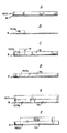
【解決手段】インダクタ102は、受動自己組立て手段を含む少なくとも2個の導電性サポート110,114によって、1巻回以上が基板100の上方に懸垂された導電性ループ104からなる。一実施例では、受動自己組立て手段は、導電性サポート110,114上に設けられた高レベルの固有応力を有する層を含む。応力層は、導電性サポート110,114の構造層(例えばポリシリコン)の上に堆積される。インダクタ102のサポートなどの構造が、ある犠牲層を除去することによって製造プロセス中に「解放」されると、応力層が収縮して残留歪みを小さくする。その結果、導電性ループが付属するサポートの自由端に上向きの力がかかる。結果として、サポートおよびループが、基板100から離れて持ち上がる。
【選択図】図1
Description
・Von Arx et al., "On-Chip Coils with Integrated Cores for Remote Inductive Powering of Integrated Microsystems", Digest of Tech. Papers, 1997 Int'l. Conf. Solid-State Sensors and Actuators (Transducers '97), Chicago, III., June 16-19, 1997, pp.999-1002
・Ziaie, et al., "A Generic MicroMachined Silicon Platform for Low-Power, Low Loss Miniature Transceivers", Digest of Tech. Papers, 1997 Int'l. Conf. Solid-State Sensors and Actuators (Transducers '97), Chicago, III., June 16-19, 1997, pp.257-260
を参照)。
[1] ZL=jXL=2πjfL
ただし、
ZLはインピーダンス(単位:オーム)、
jは虚数単位=(−1)0.5、
XLは誘導性リアクタンス(単位:オーム)、
fは周波数(単位:ヘルツ)、
Lはインダクタンス(単位:ヘンリー)、
である。容量性インピーダンスは次のように表される。
[2] ZC=jXC=1/(2πjfC)
ただし、
ZCはインピーダンス(単位:オーム)、
jは虚数単位=(−1)0.5、
XCは容量性リアクタンス(単位:オーム)、
fは周波数(単位:ヘルツ)、
Cはキャパシタンス(単位:ファラド)、
である。
[3] ZL=RL+jXL
[4] ZIN=RIN+jXIN
であり、
ZLは負荷のインピーダンス、
RLは負荷の抵抗、
jは虚数単位=(−1)0.5、
ZLは負荷のリアクタンス、
であり、ZIN、RIN、jおよびXINは、入力デバイスINの対応する量である。
[5] RL+RIN=0
[6] XL+XIN=0
[7] XL=XL (4)+XC
ただし、
XCは容量性リアクタンス、
XL (4)は誘導性リアクタンス、
である。
[8] XC=−1/(ωC)
[9] XL=ωL
ただし、
ωは周波数、
Cはキャパシタンス、
Lはインダクタンス、
である。すると、発振周波数ωoは次式によって与えられる。
[10] ωo=1/[C(XL (4)+XIN)]
キャパシタンスCによって決定される関数−XCの大きさが変化すると、発振器の周波数ωoも変化する。
102 インダクタ
104 導電性ループ
106 第1端
108 第2端
110 導電性サポート
112 第1端
114 導電性サポート
116 第1端
118 グランド接点
120 グランド接点
122 信号接点
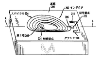
200 基板
202 インダクタ
204 スパイラル
206 第1端
208 第2端
218 グランド
220 グランド
222 信号接点
224 帰路接点
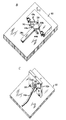
300 基板
302 インダクタ
304 スパイラル
305 セグメント
310 導電性サポート
314 導電性サポート
332 導電性ヒンジ付きプレート
334 v字形ノッチ
335 頂点
338 ヒンジ
340 導電性受動作動素子
342 v字形係合部材
343 頂点
344 ストップ
350 グランド接点
352 接点
354 グランド接点
400 基板
402 インダクタ
404 曲折ライン
406 第1端
408 第2端
410 導電性サポート
414 導電性サポート
418 グランド接点
420 グランド接点
422 信号接点
436 エッジ
444 エッジ
502 インダクタ
504 二重ループ
506 第1端
508 第2端
510 導電性サポート
514 導電性サポート
518 グランド接点
520 グランド接点
522 信号接点
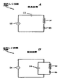
600a 回路
600b インピーダンス整合回路
750S 直列LC回路
750P 並列LC回路
800 トランシーバ
802 受信器
804 信号
806 アンテナ
808 RFバンドパスフィルタ
810 信号
812 低ノイズ増幅器
814 増幅信号
816 第1ダウンコンバータ
818 局部発振器
820 ミキサ
822 第1中間周波数バンドパスフィルタ
826 第1中間周波数増幅器
828 第2ダウンコンバータ
834 第2中間周波数バンドパスフィルタ
836 第2中間周波数増幅器
838 復調器
840 送信器
842 メッセージ
844 変調器
846 局部発振器
848 キャリア信号
850 信号
852 アップコンバータ
854 局部発振器
856 ミキサ
858 バンドパスフィルタ
860 アップコンバータ
862 局部発振器
864 ミキサ
866 バンドパスフィルタ
868 増幅器
870 アンテナ
900 回路ボードレベル実装
902 回路ボード
904 チップ
906 チップ
908 チップ
910 チップ
912 チップ
Claims (23)
- インダクタを有する物品において、前記インダクタは、
基板と、
ループの少なくとも一部が前記基板から離間した単一の導電性ループと、
前記ループの一部を持ち上げて、前記基板から離れるよう屈曲させて動作可能に位置付けるようにした移動可能受動自己組立手段とを有することを特徴とするインダクタを有する物品。 - 前記受動自己組立て手段は、応力層を有することを特徴とする請求項1に記載の物品。
- 前記物品は、2個の導電性サポートをさらに有し、
各導電性サポートは、前記応力層を有し、
前記導電性ループの第1端は、一方の導電性サポートの第1端に結合し、
前記導電性ループの第2端は、他方の導電性サポートの第1端に結合し、
各導電性サポートの第1端は、基板から離間していることを特徴とする請求項2に記載の物品。 - 前記導電性ループおよび前記2個の導電性サポートは、金属で被覆されたポリシリコンからなることを特徴とする請求項3に記載の物品。
- 前記導電性ループは、複数の巻回を有することを特徴とする請求項3に記載の物品。
- 前記導電性ループは、前記応力層を有し、
前記導電性ループの中線は、前記基板上にあり、
ループで前記中線上にない部分は、前記基板から離間していることを特徴とする請求項2に記載の物品。 - 前記導電性ループは、複数の巻回を有することを特徴とする請求項6に記載の物品。
- 前記物品は、
前記導電性ループを前記基板に対して面外方向に支持する導電性サポートと、
回転可能なように前記基板に支持されたヒンジ付きプレートとをさらに有し、
前記導電性サポートは、前記ヒンジ付きプレートに結合し、
前記受動自己組立て手段は、
前記ヒンジ付きプレート内のノッチと、
前記応力層を含む受動作動素子の第1端に結合した係合部材とを有し、
前記ノッチは前記係合部材を収容し、
前記受動作動素子および前記係合部材は、面外方向に前記ヒンジ付きプレートを持ち上げて支持するように動作可能であることを特徴とする請求項2に記載の物品。 - 前記導電性ループは、複数の巻回を有することを特徴とする請求項8に記載の物品。
- 前記受動自己組立てインダクタに電気的に接続されたキャパシタを有する第1LC回路を含むことを特徴とする請求項1に記載の物品。
- 前記LC回路はCMOSコンパチブルであることを特徴とする請求項10に記載の物品。
- 前記キャパシタは可変キャパシタであることを特徴とする請求項10に記載の物品。
- 前記物品は、前記第1LC回路を含むフィルタであり、
前記第1LC回路は、信号線およびグランド線に電気的に接続されることを特徴とする請求項10に記載の物品。 - 前記物品は、前記第1LC回路を含むフィルタであり、
前記第1LC回路は、信号線に直列に電気的に接続されることを特徴とする請求項10に記載の物品。 - 前記物品は、前記受動自己組立てインダクタを含む共振構造に電気的に接続された負性抵抗デバイスを有する第1発振器を含むことを特徴とする請求項1に記載の物品。
- 前記物品は、第1可変周波数発振器であり、
前記共振構造は、前記受動自己組立てインダクタに電気的に接続された可変キャパシタをさらに有することを特徴とする請求項15に記載の物品。 - 前記負性抵抗デバイスはトランジスタであることを特徴とする請求項16に記載の物品。
- 前記物品は、受信器および送信器を有するトランシーバであり、
前記受信器は、
第1周波数バンド内の相異なる周波数を有する複数の変調RFキャリア信号と、前記第1周波数バンド外の非常に広範囲の周波数をカバーする複数の不要信号とからなる第1信号を第1アンテナから受け取り、ほぼ前記第1周波数バンド内の周波数を有する信号のみからなる第2信号を出力するRFバンドパスフィルタと、
前記第2信号を増幅する第1低ノイズ増幅器と、
前記第1可変周波数発振器および第1ミキサを有し、増幅された第2信号をダウンコンバートされた信号にダウンコンバートする第1ダウンコンバータと、
前記第1ダウンコンバータからダウンコンバートされた信号を受け取り、変調RFキャリア信号のうちの1つを含む信号を出力する第1中間周波数バンドパスフィルタと、
1つの変調RFキャリア信号を受け取って増幅する第1中間周波数増幅器と、
増幅された変調RFキャリア信号を受け取って復調する復調器とを有することを特徴とする請求項16に記載の物品。 - 前記送信器は、
キャリア信号を発生する第2可変周波数発振器と、
前記キャリア信号上にメッセージを変調する変調器と、
第3可変周波数発振器および第2ミキサを有し、変調されたキャリア信号を中間周波数変調キャリア信号にアップコンバートするアップコンバータと、
前記中間周波数変調キャリア信号をフィルタリングするバンドパスフィルタと、
第4可変周波数発振器および第3ミキサを有し、フィルタリングされた中間周波数変調キャリア信号を所望の出力周波数にアップコンバートするアップコンバータと、
アップコンバートされた変調キャリア信号をフィルタリングするフィルタと、
アップコンバートされフィルタリングされた変調キャリア信号を所望のパワーレベルに増幅する増幅器とを有し、
前記第2、第3および第4可変周波数発振器はそれぞれ第2、第3および第4受動自己組立てインダクタを有する第2、第3および第4CMOSコンパチブルLC回路を有することを特徴とする請求項18に記載の物品。 - 前記フィルタは薄膜共振器であることを特徴とする請求項19に記載の物品。
- 前記トランシーバは単一のCMOSチップに実装されることを特徴とする請求項20に記載の物品。
- インダクタを含む周波数選択ネットワークと、
負荷に電気的に接続されたトランジスタと、
前記トランジスタに電気的に接続された終端ネットワークとを有する可変周波数発振器において、
前記インダクタは、
基板と、
ループの少なくとも一部が前記基板から離間した導電性ループと、
前記ループの一部を前記基板から離れて動作可能に位置付ける、移動可能受動自己組立手段とを有することを特徴とする可変周波数発振器。 - 犠牲材料を堆積するステップと、
前記犠牲材料上に構造層を堆積するステップと、
前記構造層を、ループの少なくとも一部を含む構成にパターン形成するステップと、
形成された構造層の一部の上に応力材料を堆積するステップと、
前記犠牲材料を除去するステップとからなる、インダクタの製造方法において、
前記犠牲材料が除去されると、前記応力材料が歪みを解放するように収縮することにより、前記形成された構造層の一部が屈曲して、基板から離れるほうにループを移動させることを特徴とする、インダクタの製造方法。
Applications Claiming Priority (2)
| Application Number | Priority Date | Filing Date | Title |
|---|---|---|---|
| US09/152189 | 1998-09-12 | ||
| US09/152,189 US6101371A (en) | 1998-09-12 | 1998-09-12 | Article comprising an inductor |
Related Parent Applications (1)
| Application Number | Title | Priority Date | Filing Date |
|---|---|---|---|
| JP11255686A Division JP2000150251A (ja) | 1998-09-12 | 1999-09-09 | 受動自己組立てインダクタを有する物品 |
Publications (2)
| Publication Number | Publication Date |
|---|---|
| JP2007201488A true JP2007201488A (ja) | 2007-08-09 |
| JP4880501B2 JP4880501B2 (ja) | 2012-02-22 |
Family
ID=22541875
Family Applications (2)
| Application Number | Title | Priority Date | Filing Date |
|---|---|---|---|
| JP11255686A Withdrawn JP2000150251A (ja) | 1998-09-12 | 1999-09-09 | 受動自己組立てインダクタを有する物品 |
| JP2007060148A Expired - Fee Related JP4880501B2 (ja) | 1998-09-12 | 2007-03-09 | 受動自己組立てインダクタを有する物品 |
Family Applications Before (1)
| Application Number | Title | Priority Date | Filing Date |
|---|---|---|---|
| JP11255686A Withdrawn JP2000150251A (ja) | 1998-09-12 | 1999-09-09 | 受動自己組立てインダクタを有する物品 |
Country Status (4)
| Country | Link |
|---|---|
| US (1) | US6101371A (ja) |
| EP (1) | EP0986106B1 (ja) |
| JP (2) | JP2000150251A (ja) |
| DE (1) | DE69937217T2 (ja) |
Cited By (4)
| Publication number | Priority date | Publication date | Assignee | Title |
|---|---|---|---|---|
| JP2011130083A (ja) * | 2009-12-16 | 2011-06-30 | Mitsubishi Electric Corp | 可変フィルタ |
| JPWO2010052839A1 (ja) * | 2008-11-06 | 2012-03-29 | パナソニック株式会社 | 半導体装置 |
| JP2013074496A (ja) * | 2011-09-28 | 2013-04-22 | Onkyo Corp | 分波回路 |
| JP2016208353A (ja) * | 2015-04-24 | 2016-12-08 | 三菱電機株式会社 | マルチポートスイッチ |
Families Citing this family (56)
| Publication number | Priority date | Publication date | Assignee | Title |
|---|---|---|---|---|
| US6591091B1 (en) | 1998-11-12 | 2003-07-08 | Broadcom Corporation | System and method for coarse/fine PLL adjustment |
| US6303423B1 (en) | 1998-12-21 | 2001-10-16 | Megic Corporation | Method for forming high performance system-on-chip using post passivation process |
| US8021976B2 (en) | 2002-10-15 | 2011-09-20 | Megica Corporation | Method of wire bonding over active area of a semiconductor circuit |
| US8421158B2 (en) | 1998-12-21 | 2013-04-16 | Megica Corporation | Chip structure with a passive device and method for forming the same |
| US8178435B2 (en) | 1998-12-21 | 2012-05-15 | Megica Corporation | High performance system-on-chip inductor using post passivation process |
| JP2000278042A (ja) * | 1999-03-26 | 2000-10-06 | Sony Corp | 発振回路及びチューナ |
| US6850353B1 (en) | 1999-06-11 | 2005-02-01 | University Of Hawaii | MEMS optical components |
| US6859299B1 (en) | 1999-06-11 | 2005-02-22 | Jung-Chih Chiao | MEMS optical components |
| WO2000077556A1 (en) * | 1999-06-11 | 2000-12-21 | University Of Hawaii | Mems optical components |
| US7151298B1 (en) * | 1999-12-20 | 2006-12-19 | Advanced Micro Devices, Inc. | Electrostatic discharge protection network having distributed components |
| JP2001274528A (ja) | 2000-01-21 | 2001-10-05 | Fujitsu Ltd | 薄膜デバイスの基板間転写方法 |
| US6392524B1 (en) * | 2000-06-09 | 2002-05-21 | Xerox Corporation | Photolithographically-patterned out-of-plane coil structures and method of making |
| US6531947B1 (en) | 2000-09-12 | 2003-03-11 | 3M Innovative Properties Company | Direct acting vertical thermal actuator with controlled bending |
| US6708491B1 (en) | 2000-09-12 | 2004-03-23 | 3M Innovative Properties Company | Direct acting vertical thermal actuator |
| US6483419B1 (en) | 2000-09-12 | 2002-11-19 | 3M Innovative Properties Company | Combination horizontal and vertical thermal actuator |
| US6683508B1 (en) | 2000-09-22 | 2004-01-27 | Agere Systems, Inc. | System and method of increasing a self-resonant frequency of a tuning circuit and an oscillator employing the same |
| US6706202B1 (en) * | 2000-09-28 | 2004-03-16 | Xerox Corporation | Method for shaped optical MEMS components with stressed thin films |
| WO2002044078A1 (en) * | 2000-11-28 | 2002-06-06 | Trustees Of Boston University | Method of manufacturing ultra-precise, self-assembled micro systems |
| DE60138221D1 (de) * | 2000-12-11 | 2009-05-14 | Koninkl Philips Electronics Nv | Bandspule |
| US6968743B2 (en) * | 2001-01-22 | 2005-11-29 | Integrated Sensing Systems, Inc. | Implantable sensing device for physiologic parameter measurement |
| US6595787B2 (en) | 2001-02-09 | 2003-07-22 | Xerox Corporation | Low cost integrated out-of-plane micro-device structures and method of making |
| US6655964B2 (en) | 2001-02-09 | 2003-12-02 | Xerox Corporation | Low cost integrated out-of-plane micro-device structures and method of making |
| US6438954B1 (en) | 2001-04-27 | 2002-08-27 | 3M Innovative Properties Company | Multi-directional thermal actuator |
| US6922127B2 (en) * | 2001-05-23 | 2005-07-26 | The Trustees Of The University Of Illinois | Raised on-chip inductor and method of manufacturing same |
| US6543087B2 (en) | 2001-06-01 | 2003-04-08 | Aip Networks, Inc. | Micro-electromechanical hinged flap structure |
| US6759275B1 (en) | 2001-09-04 | 2004-07-06 | Megic Corporation | Method for making high-performance RF integrated circuits |
| DE10159415B4 (de) * | 2001-12-04 | 2012-10-04 | MAX-PLANCK-Gesellschaft zur Förderung der Wissenschaften e.V. | Verfahren zur Herstellung einer Mikrospule und Mikrospule |
| US6781239B1 (en) * | 2001-12-05 | 2004-08-24 | National Semiconductor Corporation | Integrated circuit and method of forming the integrated circuit having a die with high Q inductors and capacitors attached to a die with a circuit as a flip chip |
| US7011530B2 (en) * | 2002-05-24 | 2006-03-14 | Sitaraman Suresh K | Multi-axis compliance spring |
| EP1540839A4 (en) * | 2002-08-20 | 2008-01-02 | Lockheed Corp | METHOD AND APPARATUS FOR MODIFYING A RADIOFREQUENCY RESPONSE |
| US6856499B2 (en) | 2003-03-28 | 2005-02-15 | Northrop Gurmman Corporation | MEMS variable inductor and capacitor |
| US6862441B2 (en) * | 2003-06-09 | 2005-03-01 | Nokia Corporation | Transmitter filter arrangement for multiband mobile phone |
| JP2005057270A (ja) * | 2003-08-01 | 2005-03-03 | Stmicroelectronics Sa | 切換え可能なインダクタンス |
| WO2005055363A1 (en) * | 2003-12-08 | 2005-06-16 | Cochlear Limited | Cochlear implant assembly |
| US7262680B2 (en) * | 2004-02-27 | 2007-08-28 | Illinois Institute Of Technology | Compact inductor with stacked via magnetic cores for integrated circuits |
| US8384189B2 (en) | 2005-03-29 | 2013-02-26 | Megica Corporation | High performance system-on-chip using post passivation process |
| KR20080002933A (ko) * | 2005-04-08 | 2008-01-04 | 엔엑스피 비 브이 | 전기발진신호 발생 전자 장치 및 방법 |
| DE102005030384B3 (de) * | 2005-06-29 | 2006-11-02 | Siemens Ag | Antennevorrichtung für Funk basierte Telefone |
| CN102157494B (zh) | 2005-07-22 | 2013-05-01 | 米辑电子股份有限公司 | 线路组件 |
| US7410894B2 (en) * | 2005-07-27 | 2008-08-12 | International Business Machines Corporation | Post last wiring level inductor using patterned plate process |
| KR100620812B1 (ko) * | 2005-08-08 | 2006-09-07 | 삼성전자주식회사 | 웨이퍼 레벨 재배선으로 형성된 터미네이션 회로선을 갖는반도체 소자 |
| JP4893112B2 (ja) * | 2006-06-03 | 2012-03-07 | 株式会社ニコン | 高周波回路コンポーネント |
| US20080001700A1 (en) * | 2006-06-30 | 2008-01-03 | Flavio Pardo | High inductance, out-of-plane inductors |
| US20080027311A1 (en) * | 2006-07-14 | 2008-01-31 | General Electric Company | Resonant transponder using self-resonance of coil |
| US7839242B1 (en) | 2006-08-23 | 2010-11-23 | National Semiconductor Corporation | Magnetic MEMS switching regulator |
| US20080102906A1 (en) * | 2006-10-30 | 2008-05-01 | Phonak Ag | Communication system and method of operating the same |
| US8749021B2 (en) | 2006-12-26 | 2014-06-10 | Megit Acquisition Corp. | Voltage regulator integrated with semiconductor chip |
| US7710232B1 (en) * | 2007-05-09 | 2010-05-04 | Sandia Corporation | Microelectromechanical tunable inductor |
| WO2009009827A1 (en) * | 2007-07-17 | 2009-01-22 | Cochlear Limited | Method and apparatus for forming an electrically insulating structure having holes for feedthroughs |
| US7936240B2 (en) * | 2007-08-16 | 2011-05-03 | Simon Fraser University | Lithographically controlled curvature for MEMS devices and antennas |
| KR101578952B1 (ko) | 2007-11-16 | 2015-12-28 | 코치리어 리미티드 | 자극 메디컬 디바이스용 전극 어레이의 제조 |
| FR2937422B1 (fr) * | 2008-10-22 | 2010-12-10 | Total Raffinage Marketing | Dispositif pour le controle de la qualite d'un lubrifiant et procede pour le controle du fonctionnement d'un equipement industriel utilisant un lubrifiant |
| JP5335931B2 (ja) | 2008-12-26 | 2013-11-06 | メギカ・コーポレイション | 電力管理集積回路を有するチップ・パッケージおよび関連技術 |
| US8373543B2 (en) * | 2009-12-22 | 2013-02-12 | Bae Systems Information And Electronic Systems Integrations Inc. | RFID transponder using ambient radiation |
| CN102870175B (zh) | 2010-02-19 | 2014-06-04 | 王明亮 | 硅基功率电感 |
| US8909188B2 (en) * | 2012-10-31 | 2014-12-09 | Cambridge Silicon Radio, Ltd. | Mixer |
Citations (3)
| Publication number | Priority date | Publication date | Assignee | Title |
|---|---|---|---|---|
| JPS52113348U (ja) * | 1976-02-26 | 1977-08-29 | ||
| JPH05159938A (ja) * | 1991-12-02 | 1993-06-25 | Murata Mfg Co Ltd | インダクタンス可変コイル |
| JPH08222694A (ja) * | 1995-02-13 | 1996-08-30 | Toshiba Corp | 半導体装置および半導体装置の製造方法 |
Family Cites Families (10)
| Publication number | Priority date | Publication date | Assignee | Title |
|---|---|---|---|---|
| US3932824A (en) * | 1970-03-06 | 1976-01-13 | Wycoff Keith H | Signal selective circuit |
| US3697911A (en) * | 1971-01-20 | 1972-10-10 | William A Strauss Jr | Coil form |
| US4733190A (en) * | 1987-03-16 | 1988-03-22 | Medical Advances, Inc. | NMR local coil with adjustable spacing |
| US5437057A (en) * | 1992-12-03 | 1995-07-25 | Xerox Corporation | Wireless communications using near field coupling |
| WO1994017558A1 (en) * | 1993-01-29 | 1994-08-04 | The Regents Of The University Of California | Monolithic passive component |
| DE4418432A1 (de) * | 1994-05-26 | 1995-11-30 | Siemens Ag | Frequenzveränderbare Oszillatoranordnung |
| DE4437260C1 (de) * | 1994-10-18 | 1995-10-19 | Siemens Ag | Mikromechanisches Relais |
| SE9500849D0 (sv) * | 1995-03-10 | 1995-03-10 | Pharmacia Ab | Methods for the manufacturing of micromachined structures and micromachined structures manufactured using such methods |
| JP3378435B2 (ja) * | 1995-09-29 | 2003-02-17 | 株式会社東芝 | 超高周波帯無線通信装置 |
| US5977660A (en) * | 1996-08-09 | 1999-11-02 | Mesta Electronics, Inc. | Active harmonic filter and power factor corrector |
-
1998
- 1998-09-12 US US09/152,189 patent/US6101371A/en not_active Expired - Lifetime
-
1999
- 1999-08-31 DE DE69937217T patent/DE69937217T2/de not_active Expired - Lifetime
- 1999-08-31 EP EP99306918A patent/EP0986106B1/en not_active Expired - Lifetime
- 1999-09-09 JP JP11255686A patent/JP2000150251A/ja not_active Withdrawn
-
2007
- 2007-03-09 JP JP2007060148A patent/JP4880501B2/ja not_active Expired - Fee Related
Patent Citations (3)
| Publication number | Priority date | Publication date | Assignee | Title |
|---|---|---|---|---|
| JPS52113348U (ja) * | 1976-02-26 | 1977-08-29 | ||
| JPH05159938A (ja) * | 1991-12-02 | 1993-06-25 | Murata Mfg Co Ltd | インダクタンス可変コイル |
| JPH08222694A (ja) * | 1995-02-13 | 1996-08-30 | Toshiba Corp | 半導体装置および半導体装置の製造方法 |
Cited By (4)
| Publication number | Priority date | Publication date | Assignee | Title |
|---|---|---|---|---|
| JPWO2010052839A1 (ja) * | 2008-11-06 | 2012-03-29 | パナソニック株式会社 | 半導体装置 |
| JP2011130083A (ja) * | 2009-12-16 | 2011-06-30 | Mitsubishi Electric Corp | 可変フィルタ |
| JP2013074496A (ja) * | 2011-09-28 | 2013-04-22 | Onkyo Corp | 分波回路 |
| JP2016208353A (ja) * | 2015-04-24 | 2016-12-08 | 三菱電機株式会社 | マルチポートスイッチ |
Also Published As
| Publication number | Publication date |
|---|---|
| EP0986106A1 (en) | 2000-03-15 |
| DE69937217T2 (de) | 2008-07-03 |
| JP4880501B2 (ja) | 2012-02-22 |
| DE69937217D1 (de) | 2007-11-15 |
| EP0986106B1 (en) | 2007-10-03 |
| JP2000150251A (ja) | 2000-05-30 |
| US6101371A (en) | 2000-08-08 |
Similar Documents
| Publication | Publication Date | Title |
|---|---|---|
| JP4880501B2 (ja) | 受動自己組立てインダクタを有する物品 | |
| EP1760731B1 (en) | Integrated electronic device | |
| CN1316525C (zh) | 电容可变型的电容器装置 | |
| US6184755B1 (en) | Article comprising a variable inductor | |
| JP4101763B2 (ja) | 結合器、集積電子コンポーネントおよび電子装置 | |
| US7436271B2 (en) | Dielectrically transduced single-ended to differential MEMS filter | |
| US8720023B2 (en) | Method of manufacturing a monolithic duplexer | |
| JP2005518746A (ja) | Memベースのコンピュータシステム、及びそれに用いるクロック生成発振器回路及びlcタンク装置 | |
| US7701312B2 (en) | Integrated device and fabricating method thereof | |
| JP2002094328A (ja) | 通信信号ミキシング/フィルタリング・デバイスおよびその製造方法 | |
| JP2003532320A (ja) | 振動マイクロメカニカル素子列を利用して少なくとも1つの所望の出力周波数を有する信号を生成するための方法及び装置 | |
| US20040058591A1 (en) | Electrically-coupled micro-electro-mechanical filter systems and methods | |
| Larson | Microwave MEMS technology for next-generation wireless communications | |
| US20070205849A1 (en) | Frequency-selective transformer and mixer incorporating same | |
| Nguyen | Communications applications of microelectromechanical systems | |
| JP5428771B2 (ja) | 可変分布定数線路、可変フィルタ、および通信モジュール | |
| JP2005311511A (ja) | 高周波集積回路装置 | |
| Young et al. | A micromachined RF low phase noise voltage‐controlled oscillator for wireless communications | |
| JP2005244848A (ja) | バランフィルタ | |
| JP2004350143A (ja) | バラントランス | |
| KR100393774B1 (ko) | 박막 벌크 어쿠스틱 공진기를 이용한 대역통과필터 제조방법 | |
| Lubecke et al. | High-Q MEMS for wireless integrated circuits | |
| US20090180235A1 (en) | Variable electric circuit component | |
| JP2008205793A (ja) | 高周波整合回路 | |
| Park et al. | Rf mems devices for wireless applications |
Legal Events
| Date | Code | Title | Description |
|---|---|---|---|
| A131 | Notification of reasons for refusal |
Free format text: JAPANESE INTERMEDIATE CODE: A131 Effective date: 20091005 |
|
| A601 | Written request for extension of time |
Free format text: JAPANESE INTERMEDIATE CODE: A601 Effective date: 20100105 |
|
| A602 | Written permission of extension of time |
Free format text: JAPANESE INTERMEDIATE CODE: A602 Effective date: 20100108 |
|
| A521 | Request for written amendment filed |
Free format text: JAPANESE INTERMEDIATE CODE: A523 Effective date: 20100405 |
|
| RD02 | Notification of acceptance of power of attorney |
Free format text: JAPANESE INTERMEDIATE CODE: A7422 Effective date: 20100405 |
|
| A131 | Notification of reasons for refusal |
Free format text: JAPANESE INTERMEDIATE CODE: A131 Effective date: 20101004 |
|
| A601 | Written request for extension of time |
Free format text: JAPANESE INTERMEDIATE CODE: A601 Effective date: 20110104 |
|
| A602 | Written permission of extension of time |
Free format text: JAPANESE INTERMEDIATE CODE: A602 Effective date: 20110107 |
|
| A521 | Request for written amendment filed |
Free format text: JAPANESE INTERMEDIATE CODE: A523 Effective date: 20110404 |
|
| A02 | Decision of refusal |
Free format text: JAPANESE INTERMEDIATE CODE: A02 Effective date: 20110509 |
|
| A521 | Request for written amendment filed |
Free format text: JAPANESE INTERMEDIATE CODE: A523 Effective date: 20110909 |
|
| A911 | Transfer to examiner for re-examination before appeal (zenchi) |
Free format text: JAPANESE INTERMEDIATE CODE: A911 Effective date: 20110916 |
|
| TRDD | Decision of grant or rejection written | ||
| A01 | Written decision to grant a patent or to grant a registration (utility model) |
Free format text: JAPANESE INTERMEDIATE CODE: A01 Effective date: 20111109 |
|
| A01 | Written decision to grant a patent or to grant a registration (utility model) |
Free format text: JAPANESE INTERMEDIATE CODE: A01 |
|
| A61 | First payment of annual fees (during grant procedure) |
Free format text: JAPANESE INTERMEDIATE CODE: A61 Effective date: 20111201 |
|
| R150 | Certificate of patent or registration of utility model |
Free format text: JAPANESE INTERMEDIATE CODE: R150 |
|
| FPAY | Renewal fee payment (event date is renewal date of database) |
Free format text: PAYMENT UNTIL: 20141209 Year of fee payment: 3 |
|
| R250 | Receipt of annual fees |
Free format text: JAPANESE INTERMEDIATE CODE: R250 |
|
| R250 | Receipt of annual fees |
Free format text: JAPANESE INTERMEDIATE CODE: R250 |
|
| R250 | Receipt of annual fees |
Free format text: JAPANESE INTERMEDIATE CODE: R250 |
|
| LAPS | Cancellation because of no payment of annual fees |