JP2007202000A - Horizontal/vertical synchronizing signal generation circuit - Google Patents
Horizontal/vertical synchronizing signal generation circuit Download PDFInfo
- Publication number
- JP2007202000A JP2007202000A JP2006020391A JP2006020391A JP2007202000A JP 2007202000 A JP2007202000 A JP 2007202000A JP 2006020391 A JP2006020391 A JP 2006020391A JP 2006020391 A JP2006020391 A JP 2006020391A JP 2007202000 A JP2007202000 A JP 2007202000A
- Authority
- JP
- Japan
- Prior art keywords
- signal
- circuit
- horizontal
- synchronization signal
- vertical
- Prior art date
- Legal status (The legal status is an assumption and is not a legal conclusion. Google has not performed a legal analysis and makes no representation as to the accuracy of the status listed.)
- Granted
Links
- 230000007274 generation of a signal involved in cell-cell signaling Effects 0.000 title claims description 7
- 238000000926 separation method Methods 0.000 claims description 8
- 238000010606 normalization Methods 0.000 claims description 4
- 230000001934 delay Effects 0.000 claims description 3
- 230000001360 synchronised effect Effects 0.000 abstract description 8
- 230000003111 delayed effect Effects 0.000 description 3
- 238000013459 approach Methods 0.000 description 1
- 238000010586 diagram Methods 0.000 description 1
- 238000000034 method Methods 0.000 description 1
- 230000000630 rising effect Effects 0.000 description 1
Images

Classifications
-
- H—ELECTRICITY
- H04—ELECTRIC COMMUNICATION TECHNIQUE
- H04N—PICTORIAL COMMUNICATION, e.g. TELEVISION
- H04N5/00—Details of television systems
- H04N5/04—Synchronising
- H04N5/08—Separation of synchronising signals from picture signals
- H04N5/10—Separation of line synchronising signal from frame synchronising signal or vice versa
-
- H—ELECTRICITY
- H04—ELECTRIC COMMUNICATION TECHNIQUE
- H04N—PICTORIAL COMMUNICATION, e.g. TELEVISION
- H04N5/00—Details of television systems
- H04N5/04—Synchronising
- H04N5/06—Generation of synchronising signals
Landscapes
- Engineering & Computer Science (AREA)
- Multimedia (AREA)
- Signal Processing (AREA)
- Synchronizing For Television (AREA)
Abstract
Description
本発明は、テレビ信号(TV信号)に含まれる水平および垂直同期信号に基づいて、内部で使用する水平および垂直同期信号を生成する回路に関する。 The present invention relates to a circuit for generating a horizontal and vertical synchronizing signal used internally based on a horizontal and vertical synchronizing signal included in a television signal (TV signal).
テレビ受像機やビデオ再生機などTV信号を再生する装置においては、外部から供給されるTV信号から水平および垂直同期信号を分離し、得られた水平および垂直同期信号に同期した水平および垂直同期信号を内部で発生し、この内部発生した水平および垂直同期信号を利用することで確実な同期を実現している。 In an apparatus for reproducing a TV signal such as a television receiver or a video player, a horizontal and vertical synchronizing signal synchronized with the obtained horizontal and vertical synchronizing signal is obtained by separating a horizontal and vertical synchronizing signal from an externally supplied TV signal. Is generated internally, and reliable synchronization is realized by utilizing the internally generated horizontal and vertical synchronization signals.
図4は、従来の同期信号発生回路の構成を示している。外部からのTV信号は同期分離回路10に供給され、ここで水平同期信号HSYNCと、垂直同期信号VSYCとがTV信号から分離される。水平同期信号HSYNCは、VCO/AFC回路12に供給される。このVCO/AFC回路は、内部にPLL(フェイズ・ロック・ループ)回路を有しており、供給される水平同期信号HSYNCに同期した4MHzの内部クロックを発生する。そして、この内部クロックがHカウントダウン回路14に供給される。Hカウントダウン回路14は、内部クロックをカウントして、内部で用いる水平同期信号HSを発生する。
FIG. 4 shows a configuration of a conventional synchronization signal generating circuit. An external TV signal is supplied to the
ここで、垂直帰線期間においては、1水平期間の1/2の周期の信号が必要であり、Hカウントダウン回路14は、1水平期間の2倍の周波数の信号である2×FH信号を発生する。そして、この2×FH信号は、Vカウントダウン回路16に供給される。このVカウントダウン回路16には、同期分離回路10において分離された垂直同期信号VSYNCも供給されており、この垂直同期信号VSYNCのタイミング(例えば、通常時Hレベルの垂直同期信号VSYNCの立ち下がりタイミング)が、2×FH信号に同期され、正規化された垂直同期信号VSが得られる。
Here, in the vertical blanking period, a signal having a period of ½ of one horizontal period is required, and the
このようにして得られた水平同期信号HS、垂直同期信号VSは、ディスプレイの表示タイミングの制御に使用される。 The horizontal synchronization signal HS and the vertical synchronization signal VS obtained in this way are used for controlling the display timing of the display.
ここで、上述のようにして発生した水平および垂直同期信号HS、VSは、もともとのTV信号と同様に完全に同期している。 Here, the horizontal and vertical synchronizing signals HS and VS generated as described above are completely synchronized in the same manner as the original TV signal.
ところが、映像信号処理回路においては、これら信号のタイミングが近づいてくると、HSがVSの前か後かによって、次段の回路などの垂直期間内の水平カウント数が変わり、OSD(On Screen Display)の縦揺れが発生する場合があった。 However, in the video signal processing circuit, when the timing of these signals approaches, the horizontal count number in the vertical period of the next stage circuit changes depending on whether HS is before or after VS, and OSD (On Screen Display). ) May have occurred.
本発明は、テレビ信号から水平および垂直同期信号を分離する同期分離回路と、この同期分離回路において分離された水平同期信号に内部クロックを同期させて、内部クロックに基づく内部水平同期信号を生成する水平同期信号生成回路と、前記同期分離回路において分離された垂直同期信号について前記内部クロックに基づく内部水平同期信号に基づいてタイミングを調整して正規化する正規化回路と、この正規化回路の出力である内部垂直同期信号について所定の短時間遅延する遅延回路と、を含み、生成する内部水平同期信号と内部垂直同期信号のタイミングを所定の短時間だけずらすことを特徴とする。 The present invention generates a horizontal synchronizing signal based on an internal clock by synchronizing the internal clock to the horizontal synchronizing signal separated from the television signal and the horizontal synchronizing signal separated in the synchronizing signal. A horizontal synchronization signal generation circuit; a normalization circuit that adjusts and normalizes a vertical synchronization signal separated in the synchronization separation circuit based on an internal horizontal synchronization signal based on the internal clock; and an output of the normalization circuit A delay circuit that delays the internal vertical synchronization signal for a predetermined short time, and the timing of the generated internal horizontal synchronization signal and the internal vertical synchronization signal is shifted by a predetermined short time.
本発明によれば、遅延回路によって内部垂直同期信号が遅延されることで、内部水平同期信号と内部垂直同期信号のタイミングを所定の短時間だけずらすことができる。そこで、次段の回路などにおいて、垂直期間内に安定した水平カウント数が得られ様になる。 According to the present invention, the internal vertical synchronizing signal is delayed by the delay circuit, so that the timings of the internal horizontal synchronizing signal and the internal vertical synchronizing signal can be shifted by a predetermined short time. Therefore, a stable horizontal count number can be obtained within the vertical period in the next stage circuit or the like.
以下、本発明の実施形態について、図面に基づいて説明する。 Hereinafter, embodiments of the present invention will be described with reference to the drawings.
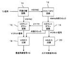
図1は、実施形態の全体構成を示す図である。従来例と同様に、外部からのTV信号は同期分離回路10に供給され、ここで水平同期信号HSYNCと、垂直同期信号VSYCとがTV信号から分離される。水平同期信号HSYNCは、VCO/AFC回路12に供給され、ここで水平同期信号HSYNCに同期した4MHzの内部クロックを発生される。そして、この内部クロックがHカウントダウン回路14に供給される。Hカウントダウン回路14は、内部クロックをカウントして、1水平期間を示すパルスであるHリセット信号を発生する。このHリセット信号は、HS出力回路20に供給され、このHS出力回路20がHリセット信号に基づいて内部で用いる水平同期信号HSを発生する。すなわち、HS出力回路20は、パルス幅調整回路を有しており、1水平期間を示すHリセット信号に基づいて設定期間だけLレベルになる水平同期信号HSを発生する。なお、同期分離回路10において得られる映像信号は、内部において発生された水平垂直同期信号のタイミングでディスプレイに表示される。
FIG. 1 is a diagram illustrating the overall configuration of the embodiment. As in the conventional example, an external TV signal is supplied to the
また、上述のように、垂直帰線期間においては、1水平期間の1/2の周期の信号が必要であり、Hカウントダウン回路14は、1水平期間の2倍の周波数の信号である2×FH信号を発生する。
Further, as described above, in the vertical blanking period, a signal having a period of ½ of one horizontal period is required, and the
ここで、水平同期信号HSが内部回路で用いる内部水平同期信号であるが、Hリセット信号や2×FH信号も水平同期のタイミングを示すものであり、本出願において内部水平同期信号に含まれる。 Here, the horizontal synchronization signal HS is an internal horizontal synchronization signal used in the internal circuit, but the H reset signal and the 2 × FH signal also indicate the timing of horizontal synchronization, and are included in the internal horizontal synchronization signal in the present application.
そして、この2×FH信号は、Vカウントダウン回路16に供給される。このVカウントダウン回路16には、同期分離回路10において分離された垂直同期信号VSYNCも供給されており、この垂直同期信号VSYNCのタイミング(例えば、通常時Hレベルの垂直同期信号VSYNCの立ち下がりタイミング)が、2×FH信号に同期され、正規化されたVリセット信号が得られる。このリセット信号は垂直同期信号VSYNCの立ち下がりタイミングが2×FH信号に同期されたものであり、Lレベルの期間は予め定められた期間になっている。
The 2 × FH signal is supplied to the
このようにして得られたVリセット信号は、VS出力回路18に供給される。このVS出力回路18は、Vリセット信号について、所定の遅延を与え、Lレベルの期間を予め設定された期間にセットし、垂直同期信号VSを生成して出力する。
The V reset signal obtained in this way is supplied to the
なお、垂直同期信号VSが内部垂直同期信号であるが、Vリセット信号も垂直同期のタイミングを示す信号であり、本出願において内部垂直同期信号に含まれる。 Although the vertical synchronization signal VS is an internal vertical synchronization signal, the V reset signal is also a signal indicating the timing of vertical synchronization, and is included in the internal vertical synchronization signal in the present application.
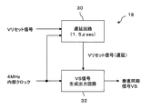
ここで、VS出力回路18の構成を図2に示す。Vリセット信号は遅延回路30に入力される。この遅延回路30には4MHzの内部クロックも供給されており、この4MHzの内部クロックを用いてVリセット信号を所定の短時間だけ遅延する。たとえば、内部クロックの6クロック分遅延することで1.5μsecの遅延となる。なお、このような遅延には直列接続されたフリップフロップが好適である。
Here, the configuration of the
遅延回路30において遅延されたVリセット信号は、VS信号生成出力回路32に供給される。このVS信号生成出力回路32には、4MHzの内部クロックも供給されており、この内部クロックのカウントによって、Vリセット信号についてのLレベル期間を所定の期間に設定し、これを垂直同期信号VSとして出力する。
The V reset signal delayed in the
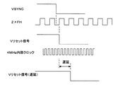
ここで、図3にVカウントダウン回路16およびVS出力回路18の遅延回路30における信号波形を模式的に示してある。
Here, FIG. 3 schematically shows signal waveforms in the
このように、Vカウントダウン回路16において、垂直同期信号VSYNCの立ち下がりが2×FH信号の立ち上がりに同期され、Vリセット信号が得られる。そして、遅延回路30においてVリセット信号の立ち下がりが4MHzの内部クロックの所定クロック分だけ遅延される。
In this way, in the
このようにして得られた水平垂直同期信号HS、VSは、次段の映像信号処理ICにおいて各種処理に使用され、ディスプレイの表示タイミングの制御に使用される。 The horizontal and vertical synchronizing signals HS and VS obtained in this way are used for various processes in the video signal processing IC in the next stage, and are used for controlling the display timing of the display.
10 同期分離回路、12 VCO/AFC回路、14 Hカウントダウン回路、16 Vカウントダウン回路、18 VS出力回路、20 HS出力回路、30 遅延回路、32 VS信号生成出力回路。 10 synchronization separation circuit, 12 VCO / AFC circuit, 14 H countdown circuit, 16 V countdown circuit, 18 VS output circuit, 20 HS output circuit, 30 delay circuit, 32 VS signal generation output circuit.
Claims (1)
この同期分離回路において分離された水平同期信号に内部クロックを同期させて、内部クロックに基づく内部水平同期信号を生成する水平同期信号生成回路と、
前記同期分離回路において分離された垂直同期信号について前記内部クロックに基づく内部水平同期信号に基づいてタイミングを調整して正規化する正規化回路と、
この正規化回路の出力である内部垂直同期信号について所定の短時間遅延する遅延回路と、
を含み、
生成する内部水平同期信号と内部垂直同期信号のタイミングを所定の短時間だけずらすことを特徴とする水平垂直同期信号生成回路。 A sync separator for separating horizontal and vertical sync signals from the television signal;
A horizontal synchronization signal generation circuit for generating an internal horizontal synchronization signal based on the internal clock by synchronizing the internal clock with the horizontal synchronization signal separated in the synchronization separation circuit;
A normalization circuit that adjusts and normalizes the timing of the vertical synchronization signal separated in the synchronization separation circuit based on the internal horizontal synchronization signal based on the internal clock;
A delay circuit that delays a predetermined short time with respect to the internal vertical synchronization signal that is an output of the normalization circuit;
Including
A horizontal / vertical synchronization signal generation circuit characterized in that the timing of the internal horizontal synchronization signal and the internal vertical synchronization signal to be generated is shifted by a predetermined short time.
Priority Applications (5)
| Application Number | Priority Date | Filing Date | Title |
|---|---|---|---|
| JP2006020391A JP4769974B2 (en) | 2006-01-30 | 2006-01-30 | Horizontal / vertical sync signal generation circuit |
| TW096102622A TWI328963B (en) | 2006-01-30 | 2007-01-24 | Horizontal and vertical synchronizing signal generating circuit |
| US11/698,754 US8223265B2 (en) | 2006-01-30 | 2007-01-26 | Horizontal and vertical synchronization signal generating circuit |
| KR1020070008837A KR100825195B1 (en) | 2006-01-30 | 2007-01-29 | Horizontal Vertical Sync Signal Generation Circuit |
| CNA2007100879199A CN101047778A (en) | 2006-01-30 | 2007-01-30 | Horizontal-vertical synchronization signal generating circuit |
Applications Claiming Priority (1)
| Application Number | Priority Date | Filing Date | Title |
|---|---|---|---|
| JP2006020391A JP4769974B2 (en) | 2006-01-30 | 2006-01-30 | Horizontal / vertical sync signal generation circuit |
Publications (2)
| Publication Number | Publication Date |
|---|---|
| JP2007202000A true JP2007202000A (en) | 2007-08-09 |
| JP4769974B2 JP4769974B2 (en) | 2011-09-07 |
Family
ID=38321707
Family Applications (1)
| Application Number | Title | Priority Date | Filing Date |
|---|---|---|---|
| JP2006020391A Expired - Fee Related JP4769974B2 (en) | 2006-01-30 | 2006-01-30 | Horizontal / vertical sync signal generation circuit |
Country Status (5)
| Country | Link |
|---|---|
| US (1) | US8223265B2 (en) |
| JP (1) | JP4769974B2 (en) |
| KR (1) | KR100825195B1 (en) |
| CN (1) | CN101047778A (en) |
| TW (1) | TWI328963B (en) |
Families Citing this family (4)
| Publication number | Priority date | Publication date | Assignee | Title |
|---|---|---|---|---|
| CN101742078B (en) * | 2008-01-31 | 2011-11-23 | 华为技术有限公司 | Synchronous clock extraction device and method therefor |
| CN102158634B (en) * | 2011-01-20 | 2012-10-31 | 凌阳科技股份有限公司 | Vertical synchronization signal separation device and method |
| JP2013034039A (en) * | 2011-07-29 | 2013-02-14 | Sony Computer Entertainment Inc | Imaging device, information processing device, information processing system, and frame data output synchronization method |
| KR102050493B1 (en) * | 2018-03-20 | 2019-12-02 | 김종덕 | Camera system capable of using an external sync signal and method of using an external synchronization signal thereof |
Citations (3)
| Publication number | Priority date | Publication date | Assignee | Title |
|---|---|---|---|---|
| JPH08149332A (en) * | 1994-11-25 | 1996-06-07 | Nec Corp | Sync-regenerator and display system using the same |
| JPH114359A (en) * | 1997-06-13 | 1999-01-06 | Matsushita Electric Ind Co Ltd | Television receiver |
| JP2001343964A (en) * | 2000-06-02 | 2001-12-14 | Mitsubishi Electric Corp | Image display device |
Family Cites Families (5)
| Publication number | Priority date | Publication date | Assignee | Title |
|---|---|---|---|---|
| DE69419055T2 (en) * | 1993-03-26 | 1999-12-23 | Sony Corp., Tokio/Tokyo | Device for generating a synchronization signal |
| JPH09154082A (en) | 1995-11-30 | 1997-06-10 | Nec Eng Ltd | Vertical sync detector |
| CN1150753C (en) | 1999-03-08 | 2004-05-19 | 明基电通股份有限公司 | Method and device for preventing OSD display area from jumping on screen |
| JP2002112067A (en) * | 2000-09-28 | 2002-04-12 | Nec Microsystems Ltd | Synchronous signal generation circuit |
| KR100792292B1 (en) * | 2005-11-03 | 2008-01-07 | 삼성전자주식회사 | An image forming apparatus for generating a stable horizontal synchronizing signal and a horizontal synchronizing signal generating method thereof |
-
2006
- 2006-01-30 JP JP2006020391A patent/JP4769974B2/en not_active Expired - Fee Related
-
2007
- 2007-01-24 TW TW096102622A patent/TWI328963B/en not_active IP Right Cessation
- 2007-01-26 US US11/698,754 patent/US8223265B2/en not_active Expired - Fee Related
- 2007-01-29 KR KR1020070008837A patent/KR100825195B1/en not_active Expired - Fee Related
- 2007-01-30 CN CNA2007100879199A patent/CN101047778A/en active Pending
Patent Citations (3)
| Publication number | Priority date | Publication date | Assignee | Title |
|---|---|---|---|---|
| JPH08149332A (en) * | 1994-11-25 | 1996-06-07 | Nec Corp | Sync-regenerator and display system using the same |
| JPH114359A (en) * | 1997-06-13 | 1999-01-06 | Matsushita Electric Ind Co Ltd | Television receiver |
| JP2001343964A (en) * | 2000-06-02 | 2001-12-14 | Mitsubishi Electric Corp | Image display device |
Also Published As
| Publication number | Publication date |
|---|---|
| TWI328963B (en) | 2010-08-11 |
| KR100825195B1 (en) | 2008-04-24 |
| US8223265B2 (en) | 2012-07-17 |
| KR20070078802A (en) | 2007-08-02 |
| JP4769974B2 (en) | 2011-09-07 |
| TW200806014A (en) | 2008-01-16 |
| US20070177057A1 (en) | 2007-08-02 |
| CN101047778A (en) | 2007-10-03 |
Similar Documents
| Publication | Publication Date | Title |
|---|---|---|
| US8233092B2 (en) | Video signal processing device | |
| KR100825195B1 (en) | Horizontal Vertical Sync Signal Generation Circuit | |
| WO2008045493A2 (en) | Clock generation with minimum number of crystals in a multimedia system | |
| US7460113B2 (en) | Digital pixel clock generation circuit and method employing independent clock | |
| US9883082B2 (en) | Timing based corrector for video | |
| JP3514067B2 (en) | Semiconductor integrated circuit | |
| US7432982B2 (en) | OSD insert circuit | |
| JP3814955B2 (en) | Synchronization signal generating circuit for television receiver and television receiver | |
| JP3405008B2 (en) | Vertical sync signal circuit | |
| CN100490541C (en) | Method for reducing phase-locked loop jitter in video applications | |
| JPS63316569A (en) | Synchronizing device | |
| JPH08180828A (en) | Synchronous clock signal generator | |
| JP2005124089A (en) | Video signal processing device | |
| JP2743428B2 (en) | Burst gate pulse generation circuit | |
| JPS63122366A (en) | Horizontally synchronizing pll circuit for television receiver | |
| JPH09312784A (en) | Vertical synchronization circuit and timing controller | |
| JPH1127559A (en) | Synchronous playback circuit | |
| JPH04188961A (en) | Phase variable phase locked loop circuit | |
| KR20010010700A (en) | Apparatus for generating Field Signal varying offset time | |
| JPH08336081A (en) | On-screen insertion device | |
| JP2010171716A (en) | Device and method for processing video signal | |
| JPS62150970A (en) | Phase synchronizing circuit | |
| KR20030030323A (en) | Separation circuit for composition sync-signal of flat pannel display | |
| JPH06284388A (en) | Synchronous processing circuit of television conversion device | |
| JPH10145638A (en) | Horizontal address generation circuit for television video signals |
Legal Events
| Date | Code | Title | Description |
|---|---|---|---|
| A621 | Written request for application examination |
Free format text: JAPANESE INTERMEDIATE CODE: A621 Effective date: 20081205 |
|
| A977 | Report on retrieval |
Free format text: JAPANESE INTERMEDIATE CODE: A971007 Effective date: 20110303 |
|
| A131 | Notification of reasons for refusal |
Free format text: JAPANESE INTERMEDIATE CODE: A131 Effective date: 20110308 |
|
| A521 | Written amendment |
Free format text: JAPANESE INTERMEDIATE CODE: A523 Effective date: 20110427 |
|
| A01 | Written decision to grant a patent or to grant a registration (utility model) |
Free format text: JAPANESE INTERMEDIATE CODE: A01 Effective date: 20110524 |
|
| A711 | Notification of change in applicant |
Free format text: JAPANESE INTERMEDIATE CODE: A711 Effective date: 20110602 |
|
| A61 | First payment of annual fees (during grant procedure) |
Free format text: JAPANESE INTERMEDIATE CODE: A61 Effective date: 20110602 |
|
| FPAY | Renewal fee payment (event date is renewal date of database) |
Free format text: PAYMENT UNTIL: 20140701 Year of fee payment: 3 |
|
| R150 | Certificate of patent or registration of utility model |
Free format text: JAPANESE INTERMEDIATE CODE: R150 |
|
| FPAY | Renewal fee payment (event date is renewal date of database) |
Free format text: PAYMENT UNTIL: 20140701 Year of fee payment: 3 |
|
| S111 | Request for change of ownership or part of ownership |
Free format text: JAPANESE INTERMEDIATE CODE: R313113 |
|
| FPAY | Renewal fee payment (event date is renewal date of database) |
Free format text: PAYMENT UNTIL: 20140701 Year of fee payment: 3 |
|
| R350 | Written notification of registration of transfer |
Free format text: JAPANESE INTERMEDIATE CODE: R350 |
|
| LAPS | Cancellation because of no payment of annual fees |