JP2007206448A - 液晶表示装置及びバックライト装置 - Google Patents
液晶表示装置及びバックライト装置 Download PDFInfo
- Publication number
- JP2007206448A JP2007206448A JP2006026202A JP2006026202A JP2007206448A JP 2007206448 A JP2007206448 A JP 2007206448A JP 2006026202 A JP2006026202 A JP 2006026202A JP 2006026202 A JP2006026202 A JP 2006026202A JP 2007206448 A JP2007206448 A JP 2007206448A
- Authority
- JP
- Japan
- Prior art keywords
- guide plate
- light guide
- liquid crystal
- corner
- light
- Prior art date
- Legal status (The legal status is an assumption and is not a legal conclusion. Google has not performed a legal analysis and makes no representation as to the accuracy of the status listed.)
- Granted
Links
Images

Classifications
-
- G—PHYSICS
- G02—OPTICS
- G02B—OPTICAL ELEMENTS, SYSTEMS OR APPARATUS
- G02B6/00—Light guides; Structural details of arrangements comprising light guides and other optical elements, e.g. couplings
- G02B6/0001—Light guides; Structural details of arrangements comprising light guides and other optical elements, e.g. couplings specially adapted for lighting devices or systems
- G02B6/0011—Light guides; Structural details of arrangements comprising light guides and other optical elements, e.g. couplings specially adapted for lighting devices or systems the light guides being planar or of plate-like form
- G02B6/0033—Means for improving the coupling-out of light from the light guide
- G02B6/0035—Means for improving the coupling-out of light from the light guide provided on the surface of the light guide or in the bulk of it
- G02B6/0036—2-D arrangement of prisms, protrusions, indentations or roughened surfaces
-
- G—PHYSICS
- G02—OPTICS
- G02F—OPTICAL DEVICES OR ARRANGEMENTS FOR THE CONTROL OF LIGHT BY MODIFICATION OF THE OPTICAL PROPERTIES OF THE MEDIA OF THE ELEMENTS INVOLVED THEREIN; NON-LINEAR OPTICS; FREQUENCY-CHANGING OF LIGHT; OPTICAL LOGIC ELEMENTS; OPTICAL ANALOGUE/DIGITAL CONVERTERS
- G02F1/00—Devices or arrangements for the control of the intensity, colour, phase, polarisation or direction of light arriving from an independent light source, e.g. switching, gating or modulating; Non-linear optics
- G02F1/01—Devices or arrangements for the control of the intensity, colour, phase, polarisation or direction of light arriving from an independent light source, e.g. switching, gating or modulating; Non-linear optics for the control of the intensity, phase, polarisation or colour
- G02F1/13—Devices or arrangements for the control of the intensity, colour, phase, polarisation or direction of light arriving from an independent light source, e.g. switching, gating or modulating; Non-linear optics for the control of the intensity, phase, polarisation or colour based on liquid crystals, e.g. single liquid crystal display cells
- G02F1/133—Constructional arrangements; Operation of liquid crystal cells; Circuit arrangements
- G02F1/1333—Constructional arrangements; Manufacturing methods
- G02F1/1335—Structural association of cells with optical devices, e.g. polarisers or reflectors
-
- G—PHYSICS
- G02—OPTICS
- G02B—OPTICAL ELEMENTS, SYSTEMS OR APPARATUS
- G02B6/00—Light guides; Structural details of arrangements comprising light guides and other optical elements, e.g. couplings
-
- G—PHYSICS
- G02—OPTICS
- G02B—OPTICAL ELEMENTS, SYSTEMS OR APPARATUS
- G02B6/00—Light guides; Structural details of arrangements comprising light guides and other optical elements, e.g. couplings
- G02B6/0001—Light guides; Structural details of arrangements comprising light guides and other optical elements, e.g. couplings specially adapted for lighting devices or systems
-
- G—PHYSICS
- G02—OPTICS
- G02B—OPTICAL ELEMENTS, SYSTEMS OR APPARATUS
- G02B6/00—Light guides; Structural details of arrangements comprising light guides and other optical elements, e.g. couplings
- G02B6/0001—Light guides; Structural details of arrangements comprising light guides and other optical elements, e.g. couplings specially adapted for lighting devices or systems
- G02B6/0011—Light guides; Structural details of arrangements comprising light guides and other optical elements, e.g. couplings specially adapted for lighting devices or systems the light guides being planar or of plate-like form
- G02B6/0033—Means for improving the coupling-out of light from the light guide
- G02B6/0058—Means for improving the coupling-out of light from the light guide varying in density, size, shape or depth along the light guide
- G02B6/0061—Means for improving the coupling-out of light from the light guide varying in density, size, shape or depth along the light guide to provide homogeneous light output intensity
-
- G—PHYSICS
- G02—OPTICS
- G02B—OPTICAL ELEMENTS, SYSTEMS OR APPARATUS
- G02B6/00—Light guides; Structural details of arrangements comprising light guides and other optical elements, e.g. couplings
- G02B6/0001—Light guides; Structural details of arrangements comprising light guides and other optical elements, e.g. couplings specially adapted for lighting devices or systems
- G02B6/0011—Light guides; Structural details of arrangements comprising light guides and other optical elements, e.g. couplings specially adapted for lighting devices or systems the light guides being planar or of plate-like form
- G02B6/0013—Means for improving the coupling-in of light from the light source into the light guide
- G02B6/0023—Means for improving the coupling-in of light from the light source into the light guide provided by one optical element, or plurality thereof, placed between the light guide and the light source, or around the light source
- G02B6/0031—Reflecting element, sheet or layer
-
- G—PHYSICS
- G02—OPTICS
- G02B—OPTICAL ELEMENTS, SYSTEMS OR APPARATUS
- G02B6/00—Light guides; Structural details of arrangements comprising light guides and other optical elements, e.g. couplings
- G02B6/0001—Light guides; Structural details of arrangements comprising light guides and other optical elements, e.g. couplings specially adapted for lighting devices or systems
- G02B6/0011—Light guides; Structural details of arrangements comprising light guides and other optical elements, e.g. couplings specially adapted for lighting devices or systems the light guides being planar or of plate-like form
- G02B6/0033—Means for improving the coupling-out of light from the light guide
- G02B6/005—Means for improving the coupling-out of light from the light guide provided by one optical element, or plurality thereof, placed on the light output side of the light guide
- G02B6/0055—Reflecting element, sheet or layer
-
- G—PHYSICS
- G02—OPTICS
- G02B—OPTICAL ELEMENTS, SYSTEMS OR APPARATUS
- G02B6/00—Light guides; Structural details of arrangements comprising light guides and other optical elements, e.g. couplings
- G02B6/0001—Light guides; Structural details of arrangements comprising light guides and other optical elements, e.g. couplings specially adapted for lighting devices or systems
- G02B6/0011—Light guides; Structural details of arrangements comprising light guides and other optical elements, e.g. couplings specially adapted for lighting devices or systems the light guides being planar or of plate-like form
- G02B6/0033—Means for improving the coupling-out of light from the light guide
- G02B6/0056—Means for improving the coupling-out of light from the light guide for producing polarisation effects, e.g. by a surface with polarizing properties or by an additional polarizing elements
-
- G—PHYSICS
- G02—OPTICS
- G02F—OPTICAL DEVICES OR ARRANGEMENTS FOR THE CONTROL OF LIGHT BY MODIFICATION OF THE OPTICAL PROPERTIES OF THE MEDIA OF THE ELEMENTS INVOLVED THEREIN; NON-LINEAR OPTICS; FREQUENCY-CHANGING OF LIGHT; OPTICAL LOGIC ELEMENTS; OPTICAL ANALOGUE/DIGITAL CONVERTERS
- G02F1/00—Devices or arrangements for the control of the intensity, colour, phase, polarisation or direction of light arriving from an independent light source, e.g. switching, gating or modulating; Non-linear optics
- G02F1/01—Devices or arrangements for the control of the intensity, colour, phase, polarisation or direction of light arriving from an independent light source, e.g. switching, gating or modulating; Non-linear optics for the control of the intensity, phase, polarisation or colour
- G02F1/13—Devices or arrangements for the control of the intensity, colour, phase, polarisation or direction of light arriving from an independent light source, e.g. switching, gating or modulating; Non-linear optics for the control of the intensity, phase, polarisation or colour based on liquid crystals, e.g. single liquid crystal display cells
- G02F1/133—Constructional arrangements; Operation of liquid crystal cells; Circuit arrangements
- G02F1/1333—Constructional arrangements; Manufacturing methods
- G02F1/1335—Structural association of cells with optical devices, e.g. polarisers or reflectors
- G02F1/133528—Polarisers
-
- G—PHYSICS
- G02—OPTICS
- G02F—OPTICAL DEVICES OR ARRANGEMENTS FOR THE CONTROL OF LIGHT BY MODIFICATION OF THE OPTICAL PROPERTIES OF THE MEDIA OF THE ELEMENTS INVOLVED THEREIN; NON-LINEAR OPTICS; FREQUENCY-CHANGING OF LIGHT; OPTICAL LOGIC ELEMENTS; OPTICAL ANALOGUE/DIGITAL CONVERTERS
- G02F2203/00—Function characteristic
- G02F2203/60—Temperature independent
Landscapes
- Physics & Mathematics (AREA)
- General Physics & Mathematics (AREA)
- Optics & Photonics (AREA)
- Nonlinear Science (AREA)
- Mathematical Physics (AREA)
- Chemical & Material Sciences (AREA)
- Crystallography & Structural Chemistry (AREA)
- Planar Illumination Modules (AREA)
- Liquid Crystal (AREA)
- Light Guides In General And Applications Therefor (AREA)
Abstract
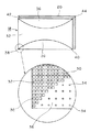
【解決手段】導光板18の裏面には、複数のドットからなる光分散ドットパターンが形成され、光分散ドットパターンは大きなドット30から構成される密領域32と小さなドット34から構成される疎領域36からなり、疎領域36は、角部38から角部40に向かって円弧状に伸びる線を境界として、長辺側に形成されているものである。
【選択図】 図2
Description
12 液晶セル
14 バックライト
16 偏光板
18 導光板
20 ランプ
30 大きなドット
32 密領域
34 小さなドット
36 疎領域
38 左下の角部
40 右下の角部
42 左上の角部
44 右上の角部
Claims (6)
- 液晶セルと、前記液晶セルに貼り付けられた偏向板と、前記液晶セルの裏面側に配されたバックライトとを有した液晶表示装置において、
前記バックライトは、導光板と、前記導光板の側部に配されたランプと、前記導光板の裏面側に配された反射板とを有し、
前記導光板の裏面には、複数のドットからなる光分散ドットパターンが形成され、
前記光分散ドットパターンは前記ドットが密な領域と疎の領域からなり、
前記疎の領域は、前記導光板の一の角部近傍から隣接する角部近傍に向かって円弧状に伸びる線を境界として、前記一の角部から前記隣接する角部に向かう辺側に形成されている
ことを特徴とする液晶表示装置。 - 液晶セルと、前記液晶セルに貼り付けられた偏向板と、前記液晶セルの裏面側に配されたバックライトとを有した液晶表示装置において、
前記バックライトは、導光板と、前記導光板の側部に配されたランプと、前記導光板の裏面側に配された反射板とを有し、
前記導光板の裏面には、複数のドットからなる光分散ドットパターンが形成され、
前記光分散ドットパターンは前記ドットが大きな領域と小さな領域からなり、
前記小さな領域は、前記導光板の一の角部近傍から隣接する角部近傍に向かって円弧状に伸びる線を境界として、前記一の角部から前記隣接する角部に向かう辺側に形成されている
ことを特徴とする液晶表示装置。 - 前記疎の領域または前記小さな領域が、前記導光板の長辺側に形成されている
ことを特徴とする請求項1または2記載の液晶表示装置。 - 前記疎の領域または前記小さな領域が、前記導光板の短辺側に形成されている
ことを特徴とする請求項1または2記載の液晶表示装置。 - 導光板と、前記導光板の側部に配されたランプと、前記導光板の裏面側に配された反射板とを有したバックライト装置において、
前記導光板の裏面には、複数のドットからなる光分散ドットパターンが形成され、
前記光分散ドットパターンは前記ドットが密な領域と疎の領域からなり、
前記疎の領域は、前記導光板の一の角部近傍から隣接する角部近傍に向かって円弧状に伸びる線を境界として、前記一の角部から前記隣接する角部に向かう辺側に形成されている
ことを特徴とするバックライト装置。 - 導光板と、前記導光板の側部に配されたランプと、前記導光板の裏面側に配された反射板とを有したバックライト装置において、
前記導光板の裏面には、複数のドットからなる光分散ドットパターンが形成され、
前記光分散ドットパターンは前記ドットが大きな領域と小さな領域からなり、
前記小さな領域は、前記導光板の一の角部近傍から隣接する角部近傍に向かって円弧状に伸びる線を境界として、前記一の角部から前記隣接する角部に向かう辺側に形成されている
ことを特徴とするバックライト装置。
Priority Applications (4)
| Application Number | Priority Date | Filing Date | Title |
|---|---|---|---|
| JP2006026202A JP4751209B2 (ja) | 2006-02-02 | 2006-02-02 | 液晶表示装置及びバックライト装置 |
| TW096101493A TW200739152A (en) | 2006-02-02 | 2007-01-15 | Liquid crystal display device and backlight device |
| US11/700,108 US20070182879A1 (en) | 2006-02-02 | 2007-01-31 | Liquid crystal display device and light source device applicable to the same |
| KR1020070010375A KR100850607B1 (ko) | 2006-02-02 | 2007-02-01 | 액정 표시 장치 및 백라이트 장치 |
Applications Claiming Priority (1)
| Application Number | Priority Date | Filing Date | Title |
|---|---|---|---|
| JP2006026202A JP4751209B2 (ja) | 2006-02-02 | 2006-02-02 | 液晶表示装置及びバックライト装置 |
Publications (2)
| Publication Number | Publication Date |
|---|---|
| JP2007206448A true JP2007206448A (ja) | 2007-08-16 |
| JP4751209B2 JP4751209B2 (ja) | 2011-08-17 |
Family
ID=38333683
Family Applications (1)
| Application Number | Title | Priority Date | Filing Date |
|---|---|---|---|
| JP2006026202A Expired - Lifetime JP4751209B2 (ja) | 2006-02-02 | 2006-02-02 | 液晶表示装置及びバックライト装置 |
Country Status (4)
| Country | Link |
|---|---|
| US (1) | US20070182879A1 (ja) |
| JP (1) | JP4751209B2 (ja) |
| KR (1) | KR100850607B1 (ja) |
| TW (1) | TW200739152A (ja) |
Citations (10)
| Publication number | Priority date | Publication date | Assignee | Title |
|---|---|---|---|---|
| JPS61145979A (ja) * | 1984-12-20 | 1986-07-03 | Toshiba Corp | 双方向catv |
| JPH06235915A (ja) * | 1993-02-12 | 1994-08-23 | Sharp Corp | 液晶表示装置 |
| JPH06242444A (ja) * | 1993-02-17 | 1994-09-02 | Sharp Corp | 液晶用照明装置 |
| JPH08220535A (ja) * | 1994-12-16 | 1996-08-30 | Canon Inc | 照明装置及びそれを用いた液晶表示装置 |
| JPH08271893A (ja) * | 1995-03-31 | 1996-10-18 | Enplas Corp | サイドライト型面光源装置 |
| JPH11231797A (ja) * | 1998-02-10 | 1999-08-27 | Omron Corp | バックライト装置用導光板、バックライト装置およびこのバックライト装置を用いた表示装置 |
| JP2002333618A (ja) * | 2001-05-07 | 2002-11-22 | Nitto Denko Corp | 反射型液晶表示装置 |
| JP2003215584A (ja) * | 2002-01-23 | 2003-07-30 | Omron Corp | 面光源装置、拡散板及び液晶表示装置 |
| JP2005513573A (ja) * | 2001-12-27 | 2005-05-12 | サムスン エレクトロニクス カンパニー リミテッド | 液晶表示装置 |
| JP2006004915A (ja) * | 2004-05-20 | 2006-01-05 | Seiko Instruments Inc | 照明装置およびこれを用いた表示装置 |
Family Cites Families (5)
| Publication number | Priority date | Publication date | Assignee | Title |
|---|---|---|---|---|
| JPH10160938A (ja) | 1996-11-29 | 1998-06-19 | Toshiba Lighting & Technol Corp | 導光ユニット、バックライト及びこれを用いた照明装置 |
| US6710829B2 (en) * | 2000-05-03 | 2004-03-23 | Benq Corporation | Method of performing a uniform illumination pattern in a back-light plate using a press |
| JP3800402B2 (ja) | 2001-08-08 | 2006-07-26 | 株式会社日立製作所 | 液晶表示装置 |
| JP2003151330A (ja) | 2001-11-12 | 2003-05-23 | Nidec Copal Corp | フロントライト及びこれを有する電子機器 |
| KR20060008600A (ko) * | 2004-07-21 | 2006-01-27 | 동양산업(주) | 부채살 패턴을 가지는 도광판 및 그 도광판 제조 방법 |
-
2006
- 2006-02-02 JP JP2006026202A patent/JP4751209B2/ja not_active Expired - Lifetime
-
2007
- 2007-01-15 TW TW096101493A patent/TW200739152A/zh unknown
- 2007-01-31 US US11/700,108 patent/US20070182879A1/en not_active Abandoned
- 2007-02-01 KR KR1020070010375A patent/KR100850607B1/ko not_active Expired - Fee Related
Patent Citations (10)
| Publication number | Priority date | Publication date | Assignee | Title |
|---|---|---|---|---|
| JPS61145979A (ja) * | 1984-12-20 | 1986-07-03 | Toshiba Corp | 双方向catv |
| JPH06235915A (ja) * | 1993-02-12 | 1994-08-23 | Sharp Corp | 液晶表示装置 |
| JPH06242444A (ja) * | 1993-02-17 | 1994-09-02 | Sharp Corp | 液晶用照明装置 |
| JPH08220535A (ja) * | 1994-12-16 | 1996-08-30 | Canon Inc | 照明装置及びそれを用いた液晶表示装置 |
| JPH08271893A (ja) * | 1995-03-31 | 1996-10-18 | Enplas Corp | サイドライト型面光源装置 |
| JPH11231797A (ja) * | 1998-02-10 | 1999-08-27 | Omron Corp | バックライト装置用導光板、バックライト装置およびこのバックライト装置を用いた表示装置 |
| JP2002333618A (ja) * | 2001-05-07 | 2002-11-22 | Nitto Denko Corp | 反射型液晶表示装置 |
| JP2005513573A (ja) * | 2001-12-27 | 2005-05-12 | サムスン エレクトロニクス カンパニー リミテッド | 液晶表示装置 |
| JP2003215584A (ja) * | 2002-01-23 | 2003-07-30 | Omron Corp | 面光源装置、拡散板及び液晶表示装置 |
| JP2006004915A (ja) * | 2004-05-20 | 2006-01-05 | Seiko Instruments Inc | 照明装置およびこれを用いた表示装置 |
Also Published As
| Publication number | Publication date |
|---|---|
| KR100850607B1 (ko) | 2008-08-05 |
| JP4751209B2 (ja) | 2011-08-17 |
| TW200739152A (en) | 2007-10-16 |
| KR20070079570A (ko) | 2007-08-07 |
| US20070182879A1 (en) | 2007-08-09 |
Similar Documents
| Publication | Publication Date | Title |
|---|---|---|
| US7637646B2 (en) | Backlight assembly and liquid crystal display device having the same | |
| JP4640188B2 (ja) | 面状光源装置 | |
| US7121692B2 (en) | Backlight module | |
| JP5394631B2 (ja) | 液晶表示装置 | |
| CN101813268B (zh) | 背光单元及使用该背光单元的液晶显示装置 | |
| KR100663297B1 (ko) | 백 라이트 유니트의 도광판 | |
| CN101688649B (zh) | 照明装置、显示装置、电视接收装置 | |
| JP2004342472A (ja) | 面状光源装置及びそれを用いた表示装置 | |
| CN101655202B (zh) | 亮度均匀性提高的背光组件 | |
| JP2004127643A (ja) | 直下型バックライト | |
| JP4461759B2 (ja) | 面発光装置および液晶表示装置 | |
| US20140307198A1 (en) | Backlight unit and liquid crystal display device including the same | |
| KR100769158B1 (ko) | 면 발광용 플랫램프 및 이를 구비한 액정표시장치 | |
| JP4751209B2 (ja) | 液晶表示装置及びバックライト装置 | |
| CN101414079B (zh) | 背光装置及液晶显示器lcd设备 | |
| KR102012387B1 (ko) | 백라이트 장치 및 이를 포함하는 액정 표시 장치 | |
| JP2009251157A (ja) | 液晶表示装置 | |
| KR101094771B1 (ko) | 직하형 액정표시장치의 백라이트 배열구조 | |
| US8330896B2 (en) | Liquid crystal display device | |
| KR100727856B1 (ko) | 발광다이오드를 광원으로 하는 직하형 백라이트의 반사판구조 및 이를 이용한 백라이트 장치 | |
| JP4504119B2 (ja) | バックライトユニットおよび液晶表示装置 | |
| KR101305364B1 (ko) | 버틈 커버 및 이를 포함한 액정표시장치 | |
| JP2007335280A (ja) | バックライトユニット及びそれを用いた液晶表示装置 | |
| JP2007298766A (ja) | 液晶表示装置 | |
| JP2012234830A (ja) | 面状光源及び液晶表示装置 |
Legal Events
| Date | Code | Title | Description |
|---|---|---|---|
| A621 | Written request for application examination |
Free format text: JAPANESE INTERMEDIATE CODE: A621 Effective date: 20080125 |
|
| A977 | Report on retrieval |
Free format text: JAPANESE INTERMEDIATE CODE: A971007 Effective date: 20110125 |
|
| A131 | Notification of reasons for refusal |
Free format text: JAPANESE INTERMEDIATE CODE: A131 Effective date: 20110222 |
|
| A521 | Request for written amendment filed |
Free format text: JAPANESE INTERMEDIATE CODE: A523 Effective date: 20110408 |
|
| TRDD | Decision of grant or rejection written | ||
| A01 | Written decision to grant a patent or to grant a registration (utility model) |
Free format text: JAPANESE INTERMEDIATE CODE: A01 Effective date: 20110426 |
|
| A61 | First payment of annual fees (during grant procedure) |
Free format text: JAPANESE INTERMEDIATE CODE: A61 Effective date: 20110520 |
|
| R150 | Certificate of patent or registration of utility model |
Ref document number: 4751209 Country of ref document: JP Free format text: JAPANESE INTERMEDIATE CODE: R150 Free format text: JAPANESE INTERMEDIATE CODE: R150 |
|
| FPAY | Renewal fee payment (event date is renewal date of database) |
Free format text: PAYMENT UNTIL: 20140527 Year of fee payment: 3 |
|
| S533 | Written request for registration of change of name |
Free format text: JAPANESE INTERMEDIATE CODE: R313533 |
|
| FPAY | Renewal fee payment (event date is renewal date of database) |
Free format text: PAYMENT UNTIL: 20140527 Year of fee payment: 3 |
|
| R350 | Written notification of registration of transfer |
Free format text: JAPANESE INTERMEDIATE CODE: R350 |
|
| R250 | Receipt of annual fees |
Free format text: JAPANESE INTERMEDIATE CODE: R250 |
|
| R250 | Receipt of annual fees |
Free format text: JAPANESE INTERMEDIATE CODE: R250 |
|
| R250 | Receipt of annual fees |
Free format text: JAPANESE INTERMEDIATE CODE: R250 |
|
| R250 | Receipt of annual fees |
Free format text: JAPANESE INTERMEDIATE CODE: R250 |
|
| R250 | Receipt of annual fees |
Free format text: JAPANESE INTERMEDIATE CODE: R250 |
|
| R250 | Receipt of annual fees |
Free format text: JAPANESE INTERMEDIATE CODE: R250 |
|
| R250 | Receipt of annual fees |
Free format text: JAPANESE INTERMEDIATE CODE: R250 |
|
| R250 | Receipt of annual fees |
Free format text: JAPANESE INTERMEDIATE CODE: R250 |
|
| S111 | Request for change of ownership or part of ownership |
Free format text: JAPANESE INTERMEDIATE CODE: R313111 |
|
| R350 | Written notification of registration of transfer |
Free format text: JAPANESE INTERMEDIATE CODE: R350 |
|
| R250 | Receipt of annual fees |
Free format text: JAPANESE INTERMEDIATE CODE: R250 |
|
| R250 | Receipt of annual fees |
Free format text: JAPANESE INTERMEDIATE CODE: R250 |
|
| R250 | Receipt of annual fees |
Free format text: JAPANESE INTERMEDIATE CODE: R250 |
|
| R250 | Receipt of annual fees |
Free format text: JAPANESE INTERMEDIATE CODE: R250 |
|
| S111 | Request for change of ownership or part of ownership |
Free format text: JAPANESE INTERMEDIATE CODE: R313113 |
|
| R350 | Written notification of registration of transfer |
Free format text: JAPANESE INTERMEDIATE CODE: R350 |
|
| EXPY | Cancellation because of completion of term |