JP2007207604A - 導電性ペースト及びその導電性ペーストを用いたセラミック多層回路基板 - Google Patents
導電性ペースト及びその導電性ペーストを用いたセラミック多層回路基板 Download PDFInfo
- Publication number
- JP2007207604A JP2007207604A JP2006025826A JP2006025826A JP2007207604A JP 2007207604 A JP2007207604 A JP 2007207604A JP 2006025826 A JP2006025826 A JP 2006025826A JP 2006025826 A JP2006025826 A JP 2006025826A JP 2007207604 A JP2007207604 A JP 2007207604A
- Authority
- JP
- Japan
- Prior art keywords
- conductive paste
- powder
- circuit board
- multilayer circuit
- wiring pattern
- Prior art date
- Legal status (The legal status is an assumption and is not a legal conclusion. Google has not performed a legal analysis and makes no representation as to the accuracy of the status listed.)
- Granted
Links
Images

Classifications
-
- H—ELECTRICITY
- H05—ELECTRIC TECHNIQUES NOT OTHERWISE PROVIDED FOR
- H05K—PRINTED CIRCUITS; CASINGS OR CONSTRUCTIONAL DETAILS OF ELECTRIC APPARATUS; MANUFACTURE OF ASSEMBLAGES OF ELECTRICAL COMPONENTS
- H05K1/00—Printed circuits
- H05K1/02—Details
- H05K1/09—Use of materials for the conductive, e.g. metallic pattern
- H05K1/092—Dispersed materials, e.g. conductive pastes or inks
-
- H—ELECTRICITY
- H05—ELECTRIC TECHNIQUES NOT OTHERWISE PROVIDED FOR
- H05K—PRINTED CIRCUITS; CASINGS OR CONSTRUCTIONAL DETAILS OF ELECTRIC APPARATUS; MANUFACTURE OF ASSEMBLAGES OF ELECTRICAL COMPONENTS
- H05K3/00—Apparatus or processes for manufacturing printed circuits
- H05K3/40—Forming printed elements for providing electric connections to or between printed circuits
- H05K3/4007—Surface contacts, e.g. bumps
- H05K3/4015—Surface contacts, e.g. bumps using auxiliary conductive elements, e.g. pieces of metal foil, metallic spheres
-
- H—ELECTRICITY
- H05—ELECTRIC TECHNIQUES NOT OTHERWISE PROVIDED FOR
- H05K—PRINTED CIRCUITS; CASINGS OR CONSTRUCTIONAL DETAILS OF ELECTRIC APPARATUS; MANUFACTURE OF ASSEMBLAGES OF ELECTRICAL COMPONENTS
- H05K3/00—Apparatus or processes for manufacturing printed circuits
- H05K3/46—Manufacturing multilayer circuits
- H05K3/4611—Manufacturing multilayer circuits by laminating two or more circuit boards
- H05K3/4623—Manufacturing multilayer circuits by laminating two or more circuit boards the circuit boards having internal via connections between two or more circuit layers before lamination, e.g. double-sided circuit boards
-
- H—ELECTRICITY
- H05—ELECTRIC TECHNIQUES NOT OTHERWISE PROVIDED FOR
- H05K—PRINTED CIRCUITS; CASINGS OR CONSTRUCTIONAL DETAILS OF ELECTRIC APPARATUS; MANUFACTURE OF ASSEMBLAGES OF ELECTRICAL COMPONENTS
- H05K3/00—Apparatus or processes for manufacturing printed circuits
- H05K3/46—Manufacturing multilayer circuits
- H05K3/4611—Manufacturing multilayer circuits by laminating two or more circuit boards
- H05K3/4626—Manufacturing multilayer circuits by laminating two or more circuit boards characterised by the insulating layers or materials
- H05K3/4629—Manufacturing multilayer circuits by laminating two or more circuit boards characterised by the insulating layers or materials laminating inorganic sheets comprising printed circuits, e.g. green ceramic sheets
-
- H—ELECTRICITY
- H05—ELECTRIC TECHNIQUES NOT OTHERWISE PROVIDED FOR
- H05K—PRINTED CIRCUITS; CASINGS OR CONSTRUCTIONAL DETAILS OF ELECTRIC APPARATUS; MANUFACTURE OF ASSEMBLAGES OF ELECTRICAL COMPONENTS
- H05K3/00—Apparatus or processes for manufacturing printed circuits
- H05K3/46—Manufacturing multilayer circuits
- H05K3/4644—Manufacturing multilayer circuits by building the multilayer layer by layer, i.e. build-up multilayer circuits
- H05K3/4664—Adding a circuit layer by thick film methods, e.g. printing techniques or by other techniques for making conductive patterns by using pastes, inks or powders
Landscapes
- Engineering & Computer Science (AREA)
- Microelectronics & Electronic Packaging (AREA)
- Manufacturing & Machinery (AREA)
- Chemical & Material Sciences (AREA)
- Ceramic Engineering (AREA)
- Inorganic Chemistry (AREA)
- Dispersion Chemistry (AREA)
- Conductive Materials (AREA)
- Production Of Multi-Layered Print Wiring Board (AREA)
- Manufacturing Of Printed Wiring (AREA)
- Parts Printed On Printed Circuit Boards (AREA)
Abstract
【解決手段】導電性粉末と、有機化合物からなるバインダ成分と、有機溶剤とを含む導電性ペーストにおいて、導電性粉末として銀粉末と酸化銀粉末とを含有している。
【選択図】なし
Description
2AgO→2Ag+O2
すなわち、酸化銀は約400℃で還元反応を起こすので、基板の焼成前に酸化銀が還元反応を起こすような温度において熱処理(脱バインダー処理)を行うことにより、還元反応の結果生成する酸素(O2)がバインダー成分である有機化合物を分解し、脱バインダーが促進される。その結果、後続する基板の焼成時に配線パターンと基板の間に隙間やクラックが発生しにくい、信頼性の高いセラミック多層回路基板を得ることができる。
(1)低温焼成セラミックグリーンシートの成形
低温焼成セラミックのグリーンシートを、ドクターブレード法等でテープ成形する。この際、低温焼成セラミックとしては、例えば、CaO−SiO2−Al2O3−B2O3 系ガ ラス50〜65重量%とアルミナ35〜50重量%との混合物を用いることができる。この他、例えば、PbO−SiO2−B2O3 系ガラスとアルミナの混合物、MgO−Al2O3−SiO2−B2O3 系ガラス、コージェライト系結晶化ガラス等の低温焼成セラミック材料を用いることもできる。
(2)グリーンシートの切断とビアホールの形成
次ぎに、テープ成形した低温焼成セラミックグリーンシートを所定の寸法に切断した後、所定の位置にビアホールをパンチング加工する。
(3)ビアホールへの導電性ペーストの充填と配線パターンの印刷
次ぎに、ビアホールへの導電性ペーストの穴埋め印刷法による充填とセラミックグリーンシート上への導電性ペーストによる配線パターンの印刷を行う。
粒径(0.3〜3.0μm)とし、後者銀粉末を比較的大粒径(3.0〜10.0μm)とすることもできる。このようにすれば、小粒径の銀粉末を用いたペーストは微細配線の形成が可能で、大粒径の銀粉末を用いたペーストは低コスト化が可能であるという効果がある。
(4)積層と圧着
ビアホールへの導電性ペーストの充填と配線パターンの印刷終了後、各層のグリーンシートを積層圧着して一体化する。
(5)脱バインダー処理
上記積層物を焼成する前に約400〜450℃に積層物を加熱して1〜2時間保持することにより、有機化合物からなるバインダー成分を酸化銀の還元反応の結果生成する酸素により熱分解して除去する。脱バインダー促進のため酸化銀粉末としてAg2O粉末およびAgO粉末の両方を含む場合の比率は、Ag2O粉末が20重量部でAgO粉末が80重量部である比率からAg2O粉末が80重量部でAgO粉末が20重量部である比率の範囲に含まれるのが好ましい。
(6)焼成
脱バインダー処理した積層物を、焼成ピーク温度800〜950℃(好ましくは、900℃前後)とし、ピーク温度で20〜60分間保持の条件で焼成し、低温焼成セラミック多層回路基板を得ることができる。
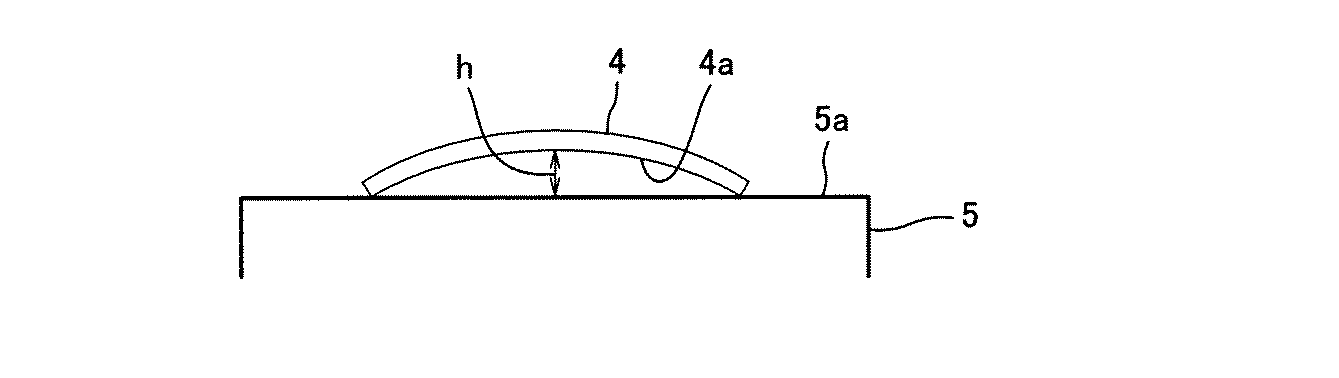
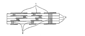
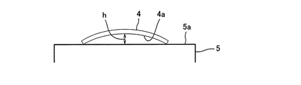
2 ビアホール
3 セラミックグリーンシート
4 セラミック基板
5 定盤
Claims (5)
- 導電性粉末と、有機化合物からなるバインダー成分と、有機溶剤とを含む導電性ペーストにおいて、導電性粉末として銀粉末と酸化銀粉末とを含有していることを特徴とする導電性ペースト。
- 銀粉末の平均粒径が0.3〜10.0μmの範囲にあることを特徴とする請求項1記載の導電性ペースト。
- 酸化銀粉末を0.1〜15.0重量%含有することを特徴とする請求項1または2記載の導電性ペースト。
- 酸化銀粉末はAg2O粉末およびAgO粉末の中から選択されたものであることを特徴とする請求項1、2または3記載の導電性ペースト。
- 請求項1、2、3または4記載の導電性ペーストを用いて導体部分を形成してなるセラミック多層回路基板。
Priority Applications (3)
| Application Number | Priority Date | Filing Date | Title |
|---|---|---|---|
| JP2006025826A JP4819516B2 (ja) | 2006-02-02 | 2006-02-02 | 導電性ペースト及びその導電性ペーストを用いたセラミック多層回路基板 |
| TW095110878A TW200731293A (en) | 2006-02-02 | 2006-03-29 | Conductive glue and ceramics multi-layer circuit substrate using such conductive glue |
| KR1020060032083A KR101118361B1 (ko) | 2006-02-02 | 2006-04-07 | 도전성 페이스트 및 그 도전성 페이스트를 이용한 세라믹 다층회로기판 제조방법 |
Applications Claiming Priority (1)
| Application Number | Priority Date | Filing Date | Title |
|---|---|---|---|
| JP2006025826A JP4819516B2 (ja) | 2006-02-02 | 2006-02-02 | 導電性ペースト及びその導電性ペーストを用いたセラミック多層回路基板 |
Publications (2)
| Publication Number | Publication Date |
|---|---|
| JP2007207604A true JP2007207604A (ja) | 2007-08-16 |
| JP4819516B2 JP4819516B2 (ja) | 2011-11-24 |
Family
ID=38486870
Family Applications (1)
| Application Number | Title | Priority Date | Filing Date |
|---|---|---|---|
| JP2006025826A Expired - Lifetime JP4819516B2 (ja) | 2006-02-02 | 2006-02-02 | 導電性ペースト及びその導電性ペーストを用いたセラミック多層回路基板 |
Country Status (3)
| Country | Link |
|---|---|
| JP (1) | JP4819516B2 (ja) |
| KR (1) | KR101118361B1 (ja) |
| TW (1) | TW200731293A (ja) |
Cited By (5)
| Publication number | Priority date | Publication date | Assignee | Title |
|---|---|---|---|---|
| JP2009088474A (ja) * | 2007-09-28 | 2009-04-23 | Samsung Electro-Mechanics Co Ltd | 印刷回路基板の層間導通方法 |
| JP2009224201A (ja) * | 2008-03-17 | 2009-10-01 | Kyoto Elex Kk | 低温焼成多層基板用導電性ペースト |
| JP2014053547A (ja) * | 2012-09-10 | 2014-03-20 | Kyoto Elex Kk | Led用セラミックパッケージ用ペースト |
| US8968608B2 (en) | 2008-01-17 | 2015-03-03 | Nichia Corporation | Method for producing conductive material, conductive material obtained by the method, electronic device containing the conductive material, light-emitting device, and method for producing light-emitting device |
| CN118342158A (zh) * | 2024-03-14 | 2024-07-16 | 广州汉源微电子封装材料有限公司 | 一种大面积封装互连用银焊膏及其制备方法与应用 |
Families Citing this family (2)
| Publication number | Priority date | Publication date | Assignee | Title |
|---|---|---|---|---|
| KR100946589B1 (ko) * | 2008-04-03 | 2010-03-09 | 엘지이노텍 주식회사 | 반도체 소자 제조용 접착 페이스트 조성물 |
| JP5849036B2 (ja) * | 2012-09-27 | 2016-01-27 | 富士フイルム株式会社 | 導電ペースト、プリント配線基板 |
Citations (4)
| Publication number | Priority date | Publication date | Assignee | Title |
|---|---|---|---|---|
| JPH0613756A (ja) * | 1992-06-25 | 1994-01-21 | Matsushita Electric Ind Co Ltd | 導体ペースト組成物 |
| JP2004281154A (ja) * | 2003-03-14 | 2004-10-07 | Fujitsu Ltd | 導体の製造方法、配線基板及びその製造方法 |
| JP2005267900A (ja) * | 2004-03-16 | 2005-09-29 | Sumitomo Osaka Cement Co Ltd | 導電性ペースト及びその製造方法 |
| JP2005293851A (ja) * | 2004-03-10 | 2005-10-20 | Toyobo Co Ltd | 導電性ペースト |
Family Cites Families (1)
| Publication number | Priority date | Publication date | Assignee | Title |
|---|---|---|---|---|
| JP2001307549A (ja) | 2000-04-21 | 2001-11-02 | Furuya Kinzoku:Kk | 銀ペースト及びその製造方法 |
-
2006
- 2006-02-02 JP JP2006025826A patent/JP4819516B2/ja not_active Expired - Lifetime
- 2006-03-29 TW TW095110878A patent/TW200731293A/zh not_active IP Right Cessation
- 2006-04-07 KR KR1020060032083A patent/KR101118361B1/ko not_active Expired - Fee Related
Patent Citations (4)
| Publication number | Priority date | Publication date | Assignee | Title |
|---|---|---|---|---|
| JPH0613756A (ja) * | 1992-06-25 | 1994-01-21 | Matsushita Electric Ind Co Ltd | 導体ペースト組成物 |
| JP2004281154A (ja) * | 2003-03-14 | 2004-10-07 | Fujitsu Ltd | 導体の製造方法、配線基板及びその製造方法 |
| JP2005293851A (ja) * | 2004-03-10 | 2005-10-20 | Toyobo Co Ltd | 導電性ペースト |
| JP2005267900A (ja) * | 2004-03-16 | 2005-09-29 | Sumitomo Osaka Cement Co Ltd | 導電性ペースト及びその製造方法 |
Cited By (11)
| Publication number | Priority date | Publication date | Assignee | Title |
|---|---|---|---|---|
| JP2009088474A (ja) * | 2007-09-28 | 2009-04-23 | Samsung Electro-Mechanics Co Ltd | 印刷回路基板の層間導通方法 |
| US8968608B2 (en) | 2008-01-17 | 2015-03-03 | Nichia Corporation | Method for producing conductive material, conductive material obtained by the method, electronic device containing the conductive material, light-emitting device, and method for producing light-emitting device |
| US20150171299A1 (en) * | 2008-01-17 | 2015-06-18 | Nichia Corporation | Method for producing conductive material, conductive material obtained by the method, electronic device containing the conductive material, light-emitting device, and method for producing light-emitting device |
| US9812624B2 (en) * | 2008-01-17 | 2017-11-07 | Nichia Corporation | Method for producing conductive material, conductive material obtained by the method, electronic device containing the conductive material, light-emitting device, and method for producing light-emitting device |
| US10573795B2 (en) | 2008-01-17 | 2020-02-25 | Nichia Corporation | Method for producing conductive material, conductive material obtained by the method, electronic device containing the conductive material, light-emitting device, and method for producing light-emitting device |
| US10950770B2 (en) | 2008-01-17 | 2021-03-16 | Nichia Corporation | Method for producing an electronic device |
| US11652197B2 (en) | 2008-01-17 | 2023-05-16 | Nichia Corporation | Method for producing an electronic device |
| JP2009224201A (ja) * | 2008-03-17 | 2009-10-01 | Kyoto Elex Kk | 低温焼成多層基板用導電性ペースト |
| JP2014053547A (ja) * | 2012-09-10 | 2014-03-20 | Kyoto Elex Kk | Led用セラミックパッケージ用ペースト |
| CN118342158A (zh) * | 2024-03-14 | 2024-07-16 | 广州汉源微电子封装材料有限公司 | 一种大面积封装互连用银焊膏及其制备方法与应用 |
| CN118342158B (zh) * | 2024-03-14 | 2025-04-11 | 广州汉源微电子封装材料有限公司 | 一种大面积封装互连用银焊膏及其制备方法与应用 |
Also Published As
| Publication number | Publication date |
|---|---|
| TW200731293A (en) | 2007-08-16 |
| KR101118361B1 (ko) | 2012-03-09 |
| TWI322995B (ja) | 2010-04-01 |
| JP4819516B2 (ja) | 2011-11-24 |
| KR20070079548A (ko) | 2007-08-07 |
Similar Documents
| Publication | Publication Date | Title |
|---|---|---|
| TWI536877B (zh) | 陶瓷通孔基板、金屬化陶瓷通孔基板、此等之製造方法 | |
| JP2006344938A (ja) | 厚膜導体組成物ならびにltcc回路およびデバイスにおけるその使用 | |
| WO2000060613A1 (en) | Conductive paste, ceramic multilayer substrate, and method for manufacturing ceramic multilayer substrate | |
| JP3422233B2 (ja) | バイアホール用導電性ペースト、およびそれを用いた積層セラミック基板の製造方法 | |
| JP4819516B2 (ja) | 導電性ペースト及びその導電性ペーストを用いたセラミック多層回路基板 | |
| JP2004047856A (ja) | 導体ペースト及び印刷方法並びにセラミック多層回路基板の製造方法 | |
| JP5364833B1 (ja) | 導体ペースト及びそれを用いたセラミック基板 | |
| JP5385070B2 (ja) | ペースト組成物 | |
| JP4385484B2 (ja) | 多層セラミック基板の製造方法および銅系導電性ペースト | |
| JP4024787B2 (ja) | フェライト多層回路基板の導電部形成用導電性ペースト及びその導電性ペーストを用いたフェライト多層回路基板 | |
| JP4732227B2 (ja) | 導電性ペースト及びその導電性ペーストを用いたセラミック多層回路基板並びにそのセラミック多層回路基板の製造方法 | |
| JP3929989B2 (ja) | 導電性ペースト及びその導電性ペーストを用いたセラミック多層回路基板。 | |
| JP4293444B2 (ja) | 導電性ペースト | |
| JP3216260B2 (ja) | 低温焼成セラミックス多層基板及びその製造方法 | |
| JP4948459B2 (ja) | ペースト組成物 | |
| JP4021787B2 (ja) | 導電性ペースト及びその導電性ペーストを用いたセラミック多層回路基板 | |
| JP4099097B2 (ja) | ビアホール充填用導電性ペースト及びその導電性ペーストを用いたセラミック多層回路基板 | |
| JP2013118119A (ja) | 導電ペースト及びそれを用いた低温焼成セラミック多層基板 | |
| JP4298558B2 (ja) | 低温焼成セラミック多層回路基板用導電性ペースト及びその導電性ペーストを用いた低温焼成セラミック多層回路基板 | |
| JP4820149B2 (ja) | 導電性ペーストの製造方法および配線基板の製造方法 | |
| JP2005116337A (ja) | 導電性ペースト、ビアホール導体及び多層セラミック基板 | |
| JP2006080363A (ja) | 導電性ペースト | |
| JPH0554718B2 (ja) | ||
| JP2004165274A (ja) | 低温焼成セラミック回路基板の製造方法 | |
| JPH066038A (ja) | 低温焼成セラミックス多層基板の製造方法 |
Legal Events
| Date | Code | Title | Description |
|---|---|---|---|
| A621 | Written request for application examination |
Free format text: JAPANESE INTERMEDIATE CODE: A621 Effective date: 20080828 |
|
| A977 | Report on retrieval |
Free format text: JAPANESE INTERMEDIATE CODE: A971007 Effective date: 20100922 |
|
| A131 | Notification of reasons for refusal |
Free format text: JAPANESE INTERMEDIATE CODE: A131 Effective date: 20100928 |
|
| A521 | Request for written amendment filed |
Free format text: JAPANESE INTERMEDIATE CODE: A523 Effective date: 20101116 |
|
| TRDD | Decision of grant or rejection written | ||
| A01 | Written decision to grant a patent or to grant a registration (utility model) |
Free format text: JAPANESE INTERMEDIATE CODE: A01 Effective date: 20110830 |
|
| A01 | Written decision to grant a patent or to grant a registration (utility model) |
Free format text: JAPANESE INTERMEDIATE CODE: A01 |
|
| A61 | First payment of annual fees (during grant procedure) |
Free format text: JAPANESE INTERMEDIATE CODE: A61 Effective date: 20110901 |
|
| FPAY | Renewal fee payment (event date is renewal date of database) |
Free format text: PAYMENT UNTIL: 20140909 Year of fee payment: 3 |
|
| R150 | Certificate of patent or registration of utility model |
Ref document number: 4819516 Country of ref document: JP Free format text: JAPANESE INTERMEDIATE CODE: R150 Free format text: JAPANESE INTERMEDIATE CODE: R150 |
|
| EXPY | Cancellation because of completion of term |