JP2007238802A - Processing method of electronic parts - Google Patents
Processing method of electronic parts Download PDFInfo
- Publication number
- JP2007238802A JP2007238802A JP2006064014A JP2006064014A JP2007238802A JP 2007238802 A JP2007238802 A JP 2007238802A JP 2006064014 A JP2006064014 A JP 2006064014A JP 2006064014 A JP2006064014 A JP 2006064014A JP 2007238802 A JP2007238802 A JP 2007238802A
- Authority
- JP
- Japan
- Prior art keywords
- adhesive tape
- electronic component
- pressure
- sensitive adhesive
- processing
- Prior art date
- Legal status (The legal status is an assumption and is not a legal conclusion. Google has not performed a legal analysis and makes no representation as to the accuracy of the status listed.)
- Pending
Links
Landscapes
- Adhesive Tapes (AREA)
- Adhesives Or Adhesive Processes (AREA)
- Mechanical Treatment Of Semiconductor (AREA)
- Dicing (AREA)
- Container, Conveyance, Adherence, Positioning, Of Wafer (AREA)
Abstract
【課題】粘着テープを用いた電子部品の加工方法であって、糊残り等を生じることなく粘着テープを剥離できる電子部品の加工方法を提供する。
【解決手段】電子部品に粘着テープを貼付する工程と、前記粘着テープが貼付された電子部品を加工する工程と、光を照射することにより前記加工後の電子部品から前記粘着テープを剥離する工程とを有する電子部品の加工方法であって、前記粘着テープは、下記式(1)で表される基を2個以上有する化合物を含有する粘着剤層を有する電子部品の加工方法。
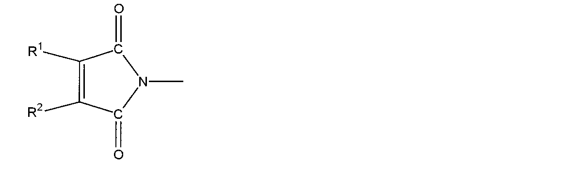
式中、R1、R2はアルキル基、アリール基、アリールアルキル基、水素原子、又はハロゲン原子を表す。
【選択図】 なしA method of processing an electronic component using an adhesive tape, which can peel the adhesive tape without causing adhesive residue or the like.
A step of attaching an adhesive tape to an electronic component, a step of processing the electronic component to which the adhesive tape is attached, and a step of peeling the adhesive tape from the processed electronic component by irradiating light. The electronic tape has a pressure-sensitive adhesive layer containing a compound having two or more groups represented by the following formula (1).
In the formula, R 1 and R 2 represent an alkyl group, an aryl group, an arylalkyl group, a hydrogen atom, or a halogen atom.
[Selection figure] None
Description
本発明は、粘着テープを用いた電子部品の加工方法であって、大気下等の酸素存在下でも紫外線等の光を照射するだけで糊残り等を生じることなく粘着テープを剥離できる電子部品の加工方法に関する。 The present invention relates to a method of processing an electronic component using an adhesive tape, which is an electronic component capable of peeling an adhesive tape without causing adhesive residue or the like only by irradiating light such as ultraviolet rays even in the presence of oxygen such as in the air. It relates to a processing method.
電子部品の製造時には、研削加工、ダイシング加工、回路転写加工、Micro Electro Mechanical Systems(MEMS)の製造等の種々の加工が施される。このような電子部品の加工方法においては、粘着テープが用いられることが多い。
例えば、半導体ウエハの研削加工においては、高純度なシリコン単結晶等から切り出した厚膜ウエハを所定の厚さにまで研削して薄膜ウエハとする場合に、厚膜ウエハを支持板に接着して補強することにより、効率よく作業を進めることが提案されている。このとき厚膜ウエハと支持板とを接着するために両面粘着テープが用いられる。また、研削済の半導体ウエハをダイシングして個々のICチップに切り分ける際には、ダイシングテープと呼ばれる粘着テープが用いられる。また、MEMS等の機械的に脆い電子部品の加工時には、加工用固定テープなどの粘着テープが用いられる。
When manufacturing electronic components, various processes such as grinding, dicing, circuit transfer, and micro electro mechanical systems (MEMS) are performed. In such an electronic component processing method, an adhesive tape is often used.
For example, in semiconductor wafer grinding, when a thick film wafer cut from a high-purity silicon single crystal or the like is ground to a predetermined thickness to form a thin film wafer, the thick film wafer is bonded to a support plate. It has been proposed to work efficiently by reinforcing. At this time, a double-sided pressure-sensitive adhesive tape is used to bond the thick film wafer and the support plate. In addition, when a ground semiconductor wafer is diced into individual IC chips, an adhesive tape called a dicing tape is used. Further, when processing mechanically brittle electronic parts such as MEMS, an adhesive tape such as a processing fixing tape is used.
電子部品の加工方法に用いられる粘着テープには、必要な間だけ強固に被着体に接着して固定できる一方で、使用後には容易に剥がせることが要求される。例えば上述の研削加工においては、粘着テープには、研削工程中には強固に接着する一方で、研削工程終了後には得られた薄膜ウエハを損傷することなく支持板から剥がせることが求められる。また、研削済の半導体ウエハをダイシングする際に用いるダイシングテープにも、ダイシング工程中には強固に接着する一方で、ダイシング工程終了後には得られたICチップを損傷することなくダイシングテープから剥がせることが求められる。特に、近年注目されている小型微小ICチップの加工時には、チップサイズが微小なのでダイシング加工後のダイシングテープからの剥離には簡単にかつ迅速に剥離できることが求められる。また、MEMS等の非常に脆い電子部品の加工時には、加工終了時には脆い部材を破壊させたり、傷を付けたりすることなく加工固定用テープから剥がすことが求められる。 The pressure-sensitive adhesive tape used in the processing method of electronic parts is required to be easily peeled off after use while it can be firmly adhered and fixed to the adherend as long as necessary. For example, in the above-described grinding process, the adhesive tape is required to be firmly bonded during the grinding process, but peeled off from the support plate without damaging the thin film wafer obtained after the grinding process is completed. In addition, it adheres firmly to the dicing tape used when dicing a ground semiconductor wafer during the dicing process, and after the dicing process is completed, the obtained IC chip can be peeled off without being damaged. Is required. In particular, when processing a small micro IC chip that has been attracting attention in recent years, since the chip size is very small, it is required to be able to easily and quickly peel off the dicing tape after dicing. Further, when processing extremely fragile electronic components such as MEMS, it is required to peel the fragile member from the processing fixing tape without damaging or scratching at the end of the processing.
これに対して特許文献1等には、(メタ)アクリル樹脂とラジカル重合開始剤とを含有する光硬化型の粘着剤からなる粘着剤層を有する粘着テープを用いた電子部品の加工方法が記載されている。このような光硬化型の粘着剤は、高い粘着性を有する一方で、紫外線等の光を照射することにより(メタ)アクリル樹脂が架橋して著しく弾性率が上昇し、粘着力が低減する性質を有する。従って、該粘着テープを用いて電子部品の加工を行った後、紫外線等の光を粘着テープに照射すれば、容易に粘着テープを剥離することができるとされている。しかしながら、実際には、紫外線を照射して粘着テープを剥離したときに、粘着テープの周辺部に糊残りが生じることがあるという問題があった。これは、酸素によりラジカル反応が阻害されることにより、空気と接する粘着テープの周辺部において充分に架橋反応が進行しないためであると考えられる。特にMEMS加工に使用される時には、加工される部品が立体的ため接着面積部分に比較して、酸素に影響を受ける周辺部の比率が大きくなるため、問題が大きい。また、小型微小ICチップの加工に使用される時にも同様に、チップサイズが微小で接着面積部分に比較して、酸素に影響を受ける周辺部の比率が大きくなるため、問題が大きい。
このような問題点を解決する方法として、例えば粘着テープの剥離工程を窒素雰囲気下で行うこと等が提案されているが、大掛かりな装置が必要な上、操作が極めて煩雑になるという問題があった。
As a method for solving such problems, for example, it has been proposed to perform the peeling process of the adhesive tape in a nitrogen atmosphere. However, a large-scale apparatus is required and the operation is extremely complicated. It was.
本発明は、上記現状に鑑み、粘着テープを用いた電子部品の加工方法であって、大気下等の酸素存在下でも紫外線等の光を照射するだけで糊残り等を生じることなく粘着テープを剥離できる電子部品の加工方法を提供することを目的とする。 In view of the above situation, the present invention is a method for processing an electronic component using an adhesive tape, and the adhesive tape is produced without causing adhesive residue or the like by simply irradiating light such as ultraviolet rays even in the presence of oxygen such as in the air. An object of the present invention is to provide a method for processing an electronic component that can be peeled off.
本発明は、電子部品に粘着テープを貼付する工程と、前記粘着テープが貼付された電子部品を加工する工程と、光を照射することにより前記加工後の電子部品から前記粘着テープを剥離する工程とを有する電子部品の加工方法であって、前記粘着テープは、重合性官能基として下記式(1)で表される基を2個以上有する化合物を含有する粘着剤層を有する電子部品の加工方法である。 The present invention includes a step of applying an adhesive tape to an electronic component, a step of processing the electronic component to which the adhesive tape is applied, and a step of peeling the adhesive tape from the processed electronic component by irradiating light. A method for processing an electronic component having a pressure-sensitive adhesive tape, wherein the adhesive tape has an adhesive layer containing a compound having two or more groups represented by the following formula (1) as a polymerizable functional group: Is the method.
以下に本発明を詳述する。 The present invention is described in detail below.
本発明の電子部品の加工方法は、電子部品に粘着テープを貼付する工程を有する。
上記電子部品としては特に限定されず、例えば、半導体ウエハ、回路パターンの材料となる金属箔、セラミックグリーンシート、絶縁性回路基板、薄ガラス基板、MEMS、超小型無線ICチップ等が挙げられる。
The processing method of the electronic component of this invention has the process of sticking an adhesive tape on an electronic component.
The electronic component is not particularly limited, and examples thereof include a semiconductor wafer, a metal foil as a circuit pattern material, a ceramic green sheet, an insulating circuit substrate, a thin glass substrate, a MEMS, and a micro wireless IC chip.
上記粘着テープは、重合性官能基として上記式(1)で表される基を2個以上有する化合物を含有する粘着剤層を有する。本発明者らは、鋭意検討の結果、重合性官能基として上記式(1)で表される基を2個以上有する化合物は、大気下であっても酸素に阻害されることなく紫外線等の光を照射することにより架橋反応を生じ、該化合物を含有する粘着剤層を有する粘着テープを用いれば、糊残り等を生じることなく粘着テープを剥離できることを見出し、本発明を完成するに至った。 The pressure-sensitive adhesive tape has a pressure-sensitive adhesive layer containing a compound having two or more groups represented by the formula (1) as a polymerizable functional group. As a result of intensive studies, the present inventors have found that a compound having two or more groups represented by the above formula (1) as a polymerizable functional group is not inhibited by oxygen even under the atmosphere, such as ultraviolet rays. When a pressure sensitive adhesive tape having a pressure sensitive adhesive layer containing the compound is generated by irradiating light, the pressure sensitive adhesive tape can be peeled off without causing adhesive residue and the like, and the present invention has been completed. .
上記重合性官能基として上記式(1)で表される基を有する化合物としては特に限定されないが、例えば、下記式(2)で表される(3,4,5,6−Tetrahydrophthalimide)ethyl acrylate等が好適である。 Although it does not specifically limit as a compound which has group represented by said Formula (1) as said polymeric functional group, For example, (3,4,5,6-Tetrahydrophthhalide) ethyl acrylate represented by following formula (2) is shown, for example. Etc. are suitable.
上記重合性官能基として上記式(1)で表される基を有する化合物は、上記式(1)で表される基以外にも水酸基、カルボキシル基等の官能基を有することが好ましい。このような官能基を有する場合には、多官能イソシアネート化合物や多官能エポキシ化合物等を用いてこれらの基と反応させることにより架橋させることが可能となり、これらの架橋により粘着剤層の凝集力を調整することが可能となる。 The compound having a group represented by the above formula (1) as the polymerizable functional group preferably has a functional group such as a hydroxyl group or a carboxyl group in addition to the group represented by the above formula (1). In the case of having such a functional group, it becomes possible to crosslink by reacting with these groups using a polyfunctional isocyanate compound or a polyfunctional epoxy compound. It becomes possible to adjust.
上記重合性官能基として上記式(1)で表される基を2個以上有する化合物としては、例えば、重合性官能基として上記式(1)で表される基を2個以上有するモノマー;重合性官能基として上記式(1)で表される基を2個以上有するオリゴマー;(メタ)アクリル樹脂、エポキシ樹脂、ウレタン樹脂、ポリエステル樹脂、オレフィン樹脂、塩化ビニル樹脂、天然ゴム、合成ゴム等の主鎖からなり、重合性官能基として上記式(1)で表される基を主鎖の末端及び/又は側鎖に有するポリマー等が挙げられる。なかでも、側鎖に上記式(1)で表される重合性官能基がグラフトされた(メタ)アクリル樹脂は、より多くの重合性官能基を導入することが可能であり、光架橋をより効果的に進行させることができることから好適である。また、側鎖に上記式(1)で表される重合性官能基がグラフトされた(メタ)アクリル樹脂は、用いる主鎖(メタ)アクリル樹脂の選択によって、化合物のガラス転移点、極性、同時に導入する官能基の種類、同時に導入する官能基の数等を自由に選択でき、粘着性能等の制御が容易であるという利点もある。
なお、上記式(1)で表される基は単一種であってもよく、複数種であってもよい。
Examples of the compound having two or more groups represented by the formula (1) as the polymerizable functional group include, for example, a monomer having two or more groups represented by the formula (1) as the polymerizable functional group; Oligomer having at least two groups represented by the above formula (1) as a functional functional group; (meth) acrylic resin, epoxy resin, urethane resin, polyester resin, olefin resin, vinyl chloride resin, natural rubber, synthetic rubber, etc. Examples thereof include a polymer having a main chain and having a group represented by the above formula (1) as a polymerizable functional group at the terminal and / or side chain of the main chain. Among them, the (meth) acrylic resin in which the polymerizable functional group represented by the above formula (1) is grafted on the side chain can introduce more polymerizable functional groups, and more photocrosslinking can be achieved. It is preferable because it can be effectively advanced. In addition, the (meth) acrylic resin grafted with the polymerizable functional group represented by the above formula (1) on the side chain has a glass transition point, a polarity, and simultaneously, depending on the selection of the main chain (meth) acrylic resin to be used. There is also an advantage that the type of functional group to be introduced, the number of functional groups to be introduced at the same time, etc. can be freely selected, and the adhesive performance and the like can be easily controlled.
In addition, the group represented by the formula (1) may be a single species or a plurality of species.
上記側鎖に上記式(1)で表される重合性官能基がグラフトされた(メタ)アクリル樹脂は、例えば、上記式(1)で表される重合性官能基とラジカル重合性の(メタ)アクリレート基とを一分子内に有する化合物と、一般に用いられる(メタ)アクリルモノマーとを、過酸化物系開始剤、アゾ化合物系開始剤、レドックス系開始剤等を開始剤として用いて、バルク重合、溶液重合、乳化重合、懸濁重合等の熱ラジカル重合法により共重合することによって調製することができる。 The (meth) acrylic resin in which the polymerizable functional group represented by the above formula (1) is grafted on the side chain is, for example, a polymerizable functional group represented by the above formula (1) and a radical polymerizable (meta ) A compound having an acrylate group in one molecule and a commonly used (meth) acrylic monomer in bulk using a peroxide initiator, an azo compound initiator, a redox initiator, etc. as an initiator It can be prepared by copolymerization by a thermal radical polymerization method such as polymerization, solution polymerization, emulsion polymerization or suspension polymerization.
上記共重合に供する(メタ)アクリルモノマーとしては特に限定されず、例えば、メチルアクリレート、エチルアクリレート、イソプロピルアクリレート、n−ブチルアクリレート、2−エチルヘキシルアクリレート、メチルメタクリレート、エチルメタクリレート、イソプロピルメタクリレート、n−ブチルメタクリレート、イソブチルメタクリレート、n−ヘキシルメタクリレート、ラウリルメタクリレート、スチレン、ビニルトルエン、酢酸ビニル、アクリロニトリル、シクロヘキシルアクリレート、ベンジルアクリレート、イソボロニルアクリレート、イソボロニルメタクリレート等が挙げられる。
また、官能基を導入するためには、上記共重合に供する(メタ)アクリルモノマーとして(メタ)アクリル酸、2−ヒドロキシエチル(メタ)アクリレート、ヒドロキシプロピル(メタ)アクリレート、4−ヒドロキシブチル(メタ)アクリレート、マレイン酸、イタコン酸、アクリルアミド、N−メチロールアクリルアミド、グリシジル(メタ)アクリレート等も用いることができる。
The (meth) acrylic monomer to be used for the copolymerization is not particularly limited. For example, methyl acrylate, ethyl acrylate, isopropyl acrylate, n-butyl acrylate, 2-ethylhexyl acrylate, methyl methacrylate, ethyl methacrylate, isopropyl methacrylate, n-butyl Examples thereof include methacrylate, isobutyl methacrylate, n-hexyl methacrylate, lauryl methacrylate, styrene, vinyl toluene, vinyl acetate, acrylonitrile, cyclohexyl acrylate, benzyl acrylate, isobornyl acrylate, and isobornyl methacrylate.
Moreover, in order to introduce a functional group, (meth) acrylic acid, 2-hydroxyethyl (meth) acrylate, hydroxypropyl (meth) acrylate, 4-hydroxybutyl (meta ) Acrylate, maleic acid, itaconic acid, acrylamide, N-methylolacrylamide, glycidyl (meth) acrylate and the like can also be used.
上記粘着剤層は、必要に応じて、(メタ)アクリル、エポキシ、ウレタン、ポリエステル、オレフィン、塩化ビニル、天然ゴム、合成ゴム等のオリゴマーやポリマーを含有してもよい。 The said adhesive layer may contain oligomers and polymers, such as (meth) acryl, epoxy, urethane, polyester, olefin, vinyl chloride, natural rubber, and synthetic rubber, as needed.
上記粘着剤層は、粘着剤層の光硬化性をより効果的に発現させるために光増感剤を含有してもよい。光増感剤を含有することによってより少ない光の照射により粘着剤層を硬化させることができる。また、より広い波長領域の光により架橋反応を生じさせることができるので、被着体がポリエチレンテレフタレート等の重合性官能基を架橋反応させる波長の光を透過しないものであっても、被着体越しに光を照射して粘着剤層を硬化させることができることから、被着体の選択の幅が広がる。
上記光増感剤としては特に限定されないが、上記重合性官能基として上記式(1)で表される基を2個以上有する化合物の感光吸収波長と粘着テープに照射する波長の両方に吸収を有するものが好適である。このような増感剤としては、例えば、チオキサントン系増感剤等が挙げられる。
The pressure-sensitive adhesive layer may contain a photosensitizer in order to more effectively express the photocurability of the pressure-sensitive adhesive layer. By containing a photosensitizer, the pressure-sensitive adhesive layer can be cured by irradiation with less light. Further, since a crosslinking reaction can be caused by light in a wider wavelength region, even if the adherend does not transmit light having a wavelength that causes a crosslinking reaction with a polymerizable functional group such as polyethylene terephthalate, the adherend Since the pressure-sensitive adhesive layer can be cured by irradiating light over the range, the selection range of the adherend is expanded.
The photosensitizer is not particularly limited, but absorbs both the photosensitive absorption wavelength of the compound having two or more groups represented by the formula (1) as the polymerizable functional group and the wavelength irradiated to the adhesive tape. What has is suitable. Examples of such sensitizers include thioxanthone sensitizers.
上記粘着剤層は、アゾ化合物、アジド化合物等の光を照射することにより気体を発生する気体発生剤を含有してもよい。このような気体発生剤を含有する粘着剤層に光を照射すると、後述のように粘着剤層全体の弾性率が上昇し、このような硬い粘着剤層中で発生した気体は粘着剤層から接着界面に放出され接着面の少なくとも一部を剥離することから、より容易に粘着テープを剥離することができる。 The said adhesive layer may contain the gas generating agent which generate | occur | produces gas by irradiating light, such as an azo compound and an azide compound. When light is applied to the pressure-sensitive adhesive layer containing such a gas generating agent, the elastic modulus of the whole pressure-sensitive adhesive layer increases as described later, and the gas generated in such a hard pressure-sensitive adhesive layer is released from the pressure-sensitive adhesive layer. Since it is released to the adhesive interface and peels at least a part of the adhesive surface, the adhesive tape can be more easily peeled off.
上記粘着剤層は、上記気体発生剤としてアジド化合物又はアゾ化合物等の光による刺激により気体を発生する気体発生剤を用いる場合には、気体発生剤への光による刺激を増幅する目的で光増感剤を含有してもよい。光増感剤を含有することによってより少ない光の照射により気体を放出させることができる。また、より広い波長領域の光により気体を放出させることができるので、被着体がポリエチレンテレフタレート等のアジド化合物から気体を発生させる波長の光を透過しないものであっても、被着体越しに光を照射して気体を発生させることができ被着体の選択の幅が広がる。
上記光増感剤としては特に限定されないが、アゾ化合物又はアジド化合物の感光吸収波長と粘着テープに照射する波長の両方に吸収を有するものが好適である。このような増感剤としては、例えば、チオキサントン系増感剤等が挙げられる。
In the case where a gas generating agent that generates a gas by light stimulation such as an azide compound or an azo compound is used as the gas generating agent, the pressure-sensitive adhesive layer is a photointensifier for the purpose of amplifying the light stimulation to the gas generating agent. You may contain a sensitizer. By containing a photosensitizer, gas can be released by irradiation with less light. In addition, since the gas can be released by light in a wider wavelength region, even if the adherend does not transmit light of a wavelength that generates gas from an azide compound such as polyethylene terephthalate, it can pass through the adherend. Gas can be generated by irradiating light, and the range of selection of adherends is expanded.
Although it does not specifically limit as said photosensitizer, What has absorption in both the photosensitive absorption wavelength of an azo compound or an azide compound and the wavelength irradiated to an adhesive tape is suitable. Examples of such sensitizers include thioxanthone sensitizers.
上記粘着剤層は、可塑剤、樹脂、界面活性剤、ワックス、微粒子充填剤等の公知の添加剤を含有してもよい。また、粘着剤の性能を損なわない範囲で、樹脂の安定性を高めるために熱安定剤、酸化防止剤を含有してもよい。このような添加剤としては、例えば、フェノール系酸化防止剤、アミン系酸化防止剤、硫黄系酸化防止剤、リン系酸化防止剤、有機スズ系安定剤、鉛系安定剤等が挙げられる。これらの添加剤は、単独で用いられてもよく、2種以上が併用されてもよい。 The pressure-sensitive adhesive layer may contain known additives such as a plasticizer, a resin, a surfactant, a wax, and a fine particle filler. Further, a heat stabilizer and an antioxidant may be contained in order to increase the stability of the resin within a range not impairing the performance of the pressure-sensitive adhesive. Examples of such additives include phenol-based antioxidants, amine-based antioxidants, sulfur-based antioxidants, phosphorus-based antioxidants, organotin-based stabilizers, lead-based stabilizers, and the like. These additives may be used independently and 2 or more types may be used together.
上記粘着剤層は、粘着剤の性能を損なわない範囲で、樹脂の光硬化性をより効果的に発現させるため光重合開始剤を含有してもよい。上記光重合開始剤としては特に限定されず、例えば、メトキシアセトフェノン等のアセトフェノン誘導体化合物;ベンゾインプロピルエーテル、ベンゾインイソブチルエーテル等のベンゾインエーテル系化合物;ベンジルジメチルケタール、アセトフェノンジエチルケタール等のケタール誘導体化合物;フォスフィンオキシド誘導体化合物;ビス(η5−シクロペンタジエニル)チタノセン誘導体化合物、ベンゾフェノン、ミヒラーケトン、クロロチオキサントン、トデシルチオキサントン、ジメチルチオキサントン、ジエチルチオキサントン、α−ヒドロキシシクロヘキシルフェニルケトン、2−ヒドロキシメチルフェニルプロパン等が挙げられる。これらの光重合開始剤は単独で用いられてもよく、2種以上が併用されてもよい。 The pressure-sensitive adhesive layer may contain a photopolymerization initiator in order to more effectively express the photocurability of the resin within a range that does not impair the performance of the pressure-sensitive adhesive. The photopolymerization initiator is not particularly limited. For example, acetophenone derivative compounds such as methoxyacetophenone; benzoin ether compounds such as benzoin propyl ether and benzoin isobutyl ether; ketal derivative compounds such as benzyldimethyl ketal and acetophenone diethyl ketal; Finoxide derivative compounds; bis (η5-cyclopentadienyl) titanocene derivative compounds, benzophenone, Michler ketone, chlorothioxanthone, todecylthioxanthone, dimethylthioxanthone, diethylthioxanthone, α-hydroxycyclohexyl phenyl ketone, 2-hydroxymethylphenylpropane, etc. Can be mentioned. These photoinitiators may be used independently and 2 or more types may be used together.
上記粘着テープは、一方の面にのみ粘着剤層が形成された片面粘着テープであってもよく、両面に粘着剤層が形成された両面粘着テープであってもよい。なお、両面粘着テープの場合、上記重合性官能基として上記式(1)で表される基を有する化合物は一方の粘着剤層にのみ含有されていてもよく、両方の粘着剤層に含有されていてもよい。 The pressure-sensitive adhesive tape may be a single-sided pressure-sensitive adhesive tape in which a pressure-sensitive adhesive layer is formed only on one surface, or may be a double-sided pressure-sensitive adhesive tape in which a pressure-sensitive adhesive layer is formed on both sides. In the case of a double-sided pressure-sensitive adhesive tape, the compound having the group represented by the formula (1) as the polymerizable functional group may be contained only in one pressure-sensitive adhesive layer, and is contained in both pressure-sensitive adhesive layers. It may be.
上記基材としては特に限定されないが、光を透過又は通過するものであることが好ましく、例えば、アクリル、オレフィン、ポリカーボネート、塩化ビニル、ABS、ポリエチレンテレフタレート(PET)、ナイロン、ウレタン、ポリイミド等の透明な樹脂からなるシート、網目状の構造を有するシート、孔が開けられたシート等が挙げられる。 Although it does not specifically limit as said base material, It is preferable that it is what permeate | transmits or passes light, For example, transparent, such as an acryl, an olefin, a polycarbonate, vinyl chloride, ABS, a polyethylene terephthalate (PET), nylon, urethane, a polyimide And a sheet made of a simple resin, a sheet having a network structure, a sheet having holes, and the like.
上記粘着テープを製造する方法としては特に限定されず、例えば、ポリエチレンテレフタレート等の基材上に、上記重合性官能基として上記式(1)で表される基を有する化合物を含有する粘着剤等をドクターナイフやスピンコーター等を用いて塗工する等の従来公知の方法を用いることができる。 The method for producing the pressure-sensitive adhesive tape is not particularly limited. For example, a pressure-sensitive adhesive containing a compound having a group represented by the formula (1) as the polymerizable functional group on a base material such as polyethylene terephthalate. A conventionally known method such as coating with a doctor knife or a spin coater can be used.
本発明の電子部品の加工方法では、次いで上記粘着テープが貼付された電子部品を加工する工程を行う。
上記加工としては特に限定されず、例えば、研削加工、ダイシング加工、回路転写加工、MEMSの製造等の通常電子部品に施される加工が挙げられる。
In the method for processing an electronic component according to the present invention, a step of processing the electronic component to which the adhesive tape is attached is then performed.
The processing is not particularly limited, and examples thereof include processing usually applied to electronic components such as grinding processing, dicing processing, circuit transfer processing, and MEMS manufacturing.
上記切削加工としては、具体的には例えば、上記粘着テープが貼付された電子部品の粘着テープが貼付されていない側の面を高速回転する研磨用砥石を用いて切削水をかけながら所望の厚さにまで研削する加工等が挙げられる。上記粘着テープが両面粘着テープである場合には、該両面粘着テープを介してガラス板や樹脂板等の支持板を貼り付けてもよい。このような支持板により補強することにより、電子部品を損傷することなく切削加工を施すことができる。 Specifically, as the cutting process, for example, a desired thickness is applied while applying cutting water using a polishing grindstone that rotates at high speed on the surface of the electronic component to which the adhesive tape is affixed. The process etc. which grind to the thickness are mentioned. When the pressure-sensitive adhesive tape is a double-sided pressure-sensitive adhesive tape, a support plate such as a glass plate or a resin plate may be attached via the double-sided pressure-sensitive adhesive tape. By reinforcing with such a support plate, cutting can be performed without damaging the electronic component.
上記ダイシング加工としては、具体的には例えば、上記粘着テープが貼付された電子部品を、ダイシングブレードを用いて切断する加工等が挙げられる。この場合、上記粘着テープは、いわゆるダイシングテープの役割を果たす。小型微小チップの微小切断加工もいわゆるダイシング加工に含まれる。 Specific examples of the dicing process include a process of cutting an electronic component to which the adhesive tape is attached using a dicing blade. In this case, the adhesive tape serves as a so-called dicing tape. Micro cutting of small micro chips is also included in so-called dicing processing.
上記回路転写加工としては、具体的には例えば、まず上記粘着テープが貼付された電子部品(金属箔)をスパッタリング等して、上記粘着テープ上に回路パターンを形成して回路転形成用転写材とし、該回路形成用転写材の回路パターン上に、半硬化状態にある絶縁性基板、又は、セラミックグリーンシートを熱プレスする加工等が挙げられる。 As the circuit transfer processing, specifically, for example, first, an electronic component (metal foil) to which the adhesive tape is attached is sputtered to form a circuit pattern on the adhesive tape to transfer a circuit transfer material. And a process of hot pressing an insulating substrate in a semi-cured state or a ceramic green sheet on the circuit pattern of the circuit-forming transfer material.
上記MEMS製造加工としては、具体的には例えば、プリンターヘッド、圧力センサ、加速度センサー、ジャイロスコープ、デジタルミラーデバイス、ガスクロマトグラフ、マイクロモーター、櫛歯型アクチュエータ、光スキャナ、カンチレバー、流路モジュール、HDDヘッド、光スイッチ、撮影素子、等の電子部品をシリコン基板上で集積化したデバイスを加工すること等が挙げられる。 Specifically, the MEMS manufacturing process includes, for example, a printer head, a pressure sensor, an acceleration sensor, a gyroscope, a digital mirror device, a gas chromatograph, a micromotor, a comb-shaped actuator, an optical scanner, a cantilever, a flow path module, and an HDD. For example, a device in which electronic components such as a head, an optical switch, and a photographing element are integrated on a silicon substrate is processed.
本発明の電子部品の加工方法では、次いで光を照射することにより上記加工後の電子部品から上記粘着テープを剥離する工程を行う。
紫外線等の光を照射することにより、上記重合性官能基として上記式(1)で表される基を有する化合物が架橋して著しく弾性率が上昇し、粘着力が低減する。このような架橋反応は、酸素によって阻害されることがないことから、従来のような窒素雰囲気下で操作を行わなくとも糊残り等を生じることなく、確実に粘着テープを剥離することができる。
In the electronic component processing method of the present invention, the step of peeling the adhesive tape from the processed electronic component is then performed by irradiating light.
By irradiating light such as ultraviolet rays, the compound having the group represented by the above formula (1) as the polymerizable functional group is cross-linked, the elastic modulus is remarkably increased, and the adhesive strength is reduced. Since such a crosslinking reaction is not hindered by oxygen, the adhesive tape can be reliably peeled off without causing adhesive residue or the like without operation in a conventional nitrogen atmosphere.
本発明によれば、粘着テープを用いた電子部品の加工方法であって、大気下等の酸素存在下でも紫外線等の光を照射するだけで糊残り等を生じることなく粘着テープを剥離できる電子部品の加工方法を提供することができる。 According to the present invention, there is provided a method for processing an electronic component using an adhesive tape, in which an adhesive tape can be peeled off without causing adhesive residue or the like only by irradiating light such as ultraviolet rays even in the presence of oxygen in the atmosphere or the like. A method of processing a part can be provided.
以下に実施例を挙げて本発明の態様を更に詳しく説明するが、本発明はこれら実施例にのみ限定されるものではない。 Hereinafter, embodiments of the present invention will be described in more detail with reference to examples. However, the present invention is not limited to these examples.
(実施例1)
(1)(3,4,5,6−Tetrahydrophthalimide)ethyl acrylateの調製
攪拌機、冷却管、水分離器を備えたフラスコに、3,4,5,6テトラヒドロフタル酸無水物304.3gとトルエン500gを仕込み、均一に溶解するまで撹拌した。
反応液を撹拌しながら油浴上で70℃に加熱し、エタノールアミン122.2gを30分かけて滴下した。その後120℃で3時間撹拌し、36gの水を共沸脱水した。
反応液を40℃に冷却後、アクリル酸158.5g、ハイドロキノンモノメチルエーテル0.15g、硫酸11.8gを加え、さらに120℃で3時間撹拌し、36gの水を共沸脱水した。
冷却後、反応液を分液ロートへ移し、400gの10%NaOH水溶液で1回、および400gの水で1回、トルエン層を洗浄した。
その後トルエン溶液をフラスコに移し、トルエンを減圧で留去し、(3,4,5,6−Tetrahydrophthalimide)ethyl acrylateを得た。
Example 1
(1) Preparation of (3,4,5,6-Tetrahydrophthalide) Ethyl acrylate In a flask equipped with a stirrer, condenser and water separator, 304.3 g of 3,4,5,6 tetrahydrophthalic anhydride and 500 g of toluene And stirred until evenly dissolved.
The reaction solution was heated to 70 ° C. on an oil bath with stirring, and 122.2 g of ethanolamine was added dropwise over 30 minutes. Thereafter, the mixture was stirred at 120 ° C. for 3 hours, and 36 g of water was azeotropically dehydrated.
After cooling the reaction solution to 40 ° C., 158.5 g of acrylic acid, 0.15 g of hydroquinone monomethyl ether, and 11.8 g of sulfuric acid were added, and the mixture was further stirred at 120 ° C. for 3 hours, and 36 g of water was azeotropically dehydrated.
After cooling, the reaction solution was transferred to a separatory funnel, and the toluene layer was washed once with 400 g of 10% NaOH aqueous solution and once with 400 g of water.
Thereafter, the toluene solution was transferred to a flask, and toluene was distilled off under reduced pressure to obtain (3,4,5,6-tetrahydrophthalimide) ethyl acrylate.
(2)光硬化型粘着剤1の調製
下記の化合物を酢酸エチルに溶解させ、混合溶液の沸点にて熱重合を行い、重量平均分子量15万のアクリル共重合体を得た。
ブチルアクリレート 85.0重量部
アクリル酸 4.5重量部
2−ヒドロキシエチルアクリレート 0.5重量部
(3,4,5,6−Tetrahydrophthalimide)ethyl acrylate 10.0重量部
1,1−ジ(t−ヘキシルパーオキシ)−3,3,5−トリメチルシクロヘキサン 0.04重量部
ジ(3,5,5−トリメチルヘキサノイル) 0.42重量部
ラウリルメルカプタン 0.1重量部
更に、反応後のアクリル共重合体を含む酢酸エチル溶液の樹脂固形分100重量部に対して、ポリイソシアネート0.3重量部を混合して、光硬化型粘着剤1の酢酸エチル溶液を調製した。
(2) Preparation of photocurable pressure-sensitive adhesive 1 The following compound was dissolved in ethyl acetate and subjected to thermal polymerization at the boiling point of the mixed solution to obtain an acrylic copolymer having a weight average molecular weight of 150,000.
Butyl acrylate 85.0 parts by weight Acrylic acid 4.5 parts by weight 2-Hydroxyethyl acrylate 0.5 parts by weight (3,4,5,6-Tetrahydrophthalimide) Ethyl acrylate 10.0 parts by weight 1,1-di (t- (Hexylperoxy) -3,3,5-trimethylcyclohexane 0.04 parts by weight di (3,5,5-trimethylhexanoyl) 0.42 parts by weight lauryl mercaptan 0.1 parts by weight A polyisocyanate 0.3 part by weight was mixed with 100 parts by weight of the resin solid content of the ethyl acetate solution containing the coalesced to prepare an ethyl acetate solution of the photocurable pressure-sensitive adhesive 1.
(3)粘着テープの作製
光硬化型粘着剤1の酢酸エチル溶液を、両面にコロナ処理を施した厚さ38μmの透明なポリエチレンテレフタレート(PET)フィルムのコロナ処理を施した面上に乾燥皮膜の厚さが約30μmとなるようにドクターナイフで塗工し、110℃、5分間加熱して溶剤を揮発させ塗工溶液を乾燥させた。乾燥後の粘着剤層は乾燥状態で粘着性を示した。乾燥後の光硬化型粘着剤1層の表面に離型処理が施されたPETフィルムをラミネートした。その後、40℃、3日間静置して養生を行った。これにより片面に粘着剤層が設けられ、その表面が離型処理が施されたPETフィルムで保護された粘着テープ1を得た。
(3) Production of pressure-sensitive adhesive tape An ethyl acetate solution of photocurable pressure-sensitive adhesive 1 was subjected to a corona treatment of a 38 μm thick transparent polyethylene terephthalate (PET) film on both sides, and a dry film was formed on the surface. Coating was performed with a doctor knife so that the thickness was about 30 μm, and the coating solution was dried by heating at 110 ° C. for 5 minutes to evaporate the solvent. The pressure-sensitive adhesive layer after drying showed adhesiveness in a dry state. A PET film having been subjected to a release treatment was laminated on the surface of one layer of the photocurable pressure-sensitive adhesive after drying. Thereafter, the film was allowed to stand at 40 ° C. for 3 days for curing. In this way, an adhesive tape 1 was obtained in which an adhesive layer was provided on one side and the surface was protected with a PET film that had been subjected to a release treatment.
(4)シリコンウエハのダイシング加工
(シリコンウエハと粘着テープとの貼り合わせ工程)
粘着テープ1の粘着剤層を保護するPETフィルムを剥がし、直径20cm、厚さ約750μmのシリコンウエハとダイシングフレームに貼り付け、ダイシングフレームに粘着テープ1を介して貼付された構成体を得た。
(4) Dicing of silicon wafer (bonding process between silicon wafer and adhesive tape)
The PET film protecting the pressure-sensitive adhesive layer of the pressure-sensitive adhesive tape 1 was peeled off and adhered to a silicon wafer having a diameter of 20 cm and a thickness of about 750 μm and a dicing frame, and a structure bonded to the dicing frame via the pressure-sensitive adhesive tape 1 was obtained.
(ダイシング工程)
ダイシングフレームに粘着テープ1を介して貼付されたシリコンウエハを、5mm角サイズのチップ状にダイシングした。
(Dicing process)
The silicon wafer affixed to the dicing frame via the adhesive tape 1 was diced into 5 mm square chips.
(粘着テープの剥離工程)
ダイシングして得たチップ状体の粘着テープ面側から、超高圧水銀灯を用いて365nmの紫外線をガラス板表面への照射強度が10mW/cm2となるよう照度を調節して1分間照射した。
紫外線照射により粘着テープの粘着力が低下し、チップのピックアップを容易に行うことができた。ピックアップしたチップを目視観察したところ、チップには糊残りは全く認められなかった。
(Adhesive tape peeling process)
From the adhesive tape surface side of the chip-like body obtained by dicing, irradiation was performed for 1 minute using an ultrahigh pressure mercury lamp while adjusting the illuminance so that the irradiation intensity to the glass plate surface was 10 mW / cm 2 .
The adhesive strength of the adhesive tape was reduced by ultraviolet irradiation, and the chip could be easily picked up. When the picked-up chip was visually observed, no adhesive residue was found on the chip.
(比較例1)
1.光硬化型粘着剤2の調製
下記の化合物を酢酸エチルに溶解させ、紫外線を照射して重合を行い、重量平均分子量70万のアクリル共重合体を得た。
イソボロニルアクリレート 80重量部
2−エチルヘキシルアクリレート 20重量部
アクリル酸 1重量部
2−ヒドロキシエチルアクリレート 5重量部
光重合開始剤 0.2重量部(イルガキュア651、50%酢酸エチル溶液)
ラウリルメルカプタン 0.01重量部
得られたアクリル共重合体を含む酢酸エチル溶液の樹脂固形分100重量部に対して、2−イソシアナトエチルメタクリレート3.5重量部を加えて反応させ、更に、反応後の酢酸エチル溶液の樹脂固形分100重量部に対して、ウレタンアクリレート(10官能)(新中村化学工業社製、NKオリゴU324A)30重量部、ポリイソシアネート0.5重量部、光重合開始剤(イルガキュア651)0.1重量部を混合し(メタ)アクリレート基を重合性反応基とする光硬化型粘着剤2の酢酸エチル溶液を調製した。
(Comparative Example 1)
1. Preparation of photocurable pressure-sensitive adhesive 2 The following compounds were dissolved in ethyl acetate and polymerized by irradiation with ultraviolet rays to obtain an acrylic copolymer having a weight average molecular weight of 700,000.
Isobonyl acrylate 80 parts by weight 2-ethylhexyl acrylate 20 parts by weight Acrylic acid 1 part by weight 2-hydroxyethyl acrylate 5 parts by weight Photopolymerization initiator 0.2 part by weight (Irgacure 651, 50% ethyl acetate solution)
0.01 parts by weight of lauryl mercaptan 0.01 parts by weight of resin solid content of 100 parts by weight of the ethyl acetate solution containing the acrylic copolymer was added and reacted with 3.5 parts by weight of 2-isocyanatoethyl methacrylate. 30 parts by weight of urethane acrylate (10 functional) (manufactured by Shin-Nakamura Chemical Co., Ltd., NK Oligo U324A), 0.5 parts by weight of polyisocyanate, photopolymerization initiator with respect to 100 parts by weight of resin solid content of the later ethyl acetate solution (Irgacure 651) 0.1 part by weight was mixed to prepare an ethyl acetate solution of the photocurable pressure-sensitive adhesive 2 having a (meth) acrylate group as a polymerizable reactive group.
(2)粘着テープの作製
光硬化型粘着剤1の代わりに光硬化型粘着剤2を用いた以外は実施例1と同様にして粘着テープ2を得た。
(3)シリコンウエハのダイシング加工
粘着テープ1の代わりに粘着テープ2を用いた以外は実施例1と同様にして、シリコンウエハと粘着テープとの貼り合わせ、ダイシングを行いチップ状体を得た。
得られたチップ状体の粘着テープ面側から、超高圧水銀灯を用いて365nmの紫外線をガラス板表面への照射強度が10mW/cm2となるよう照度を調節して1分間照射した。
紫外線照射により粘着テープの粘着力は低下し、チップのピックアップは容易に行うことができた。しかしながら、ピックアップしたチップを目視観察したところ、チップ表面の周辺部に糊残りが認められた。
(2) Preparation of pressure-sensitive adhesive tape A pressure-sensitive adhesive tape 2 was obtained in the same manner as in Example 1 except that the light-curable pressure-sensitive adhesive 2 was used instead of the light-curable pressure-sensitive adhesive 1.
(3) Dicing of silicon wafer A chip-like body was obtained by bonding and dicing a silicon wafer and an adhesive tape in the same manner as in Example 1 except that the adhesive tape 2 was used instead of the adhesive tape 1.
From the pressure-sensitive adhesive tape surface side of the obtained chip-like body, irradiation was performed for 1 minute by adjusting the illuminance so that the irradiation intensity to the surface of the glass plate was 10 mW / cm 2 using an ultrahigh pressure mercury lamp.
The adhesive strength of the adhesive tape was reduced by the ultraviolet irradiation, and the chip could be easily picked up. However, when the picked-up chip was visually observed, adhesive residue was observed in the peripheral portion of the chip surface.
本発明によれば、粘着テープを用いた電子部品の加工方法であって、大気下等の酸素存在下でも紫外線等の光を照射するだけで糊残り等を生じることなく粘着テープを剥離できる電子部品の加工方法を提供することができる。 According to the present invention, there is provided a method for processing an electronic component using an adhesive tape, in which an adhesive tape can be peeled off without causing adhesive residue or the like only by irradiating light such as ultraviolet rays even in the presence of oxygen in the atmosphere or the like. A method of processing a part can be provided.
Claims (2)
前記粘着テープは、重合性官能基として下記式(1)で表される基を2個以上有する化合物を含有する粘着剤層を有する
ことを特徴とする電子部品の加工方法。
The said adhesive tape has an adhesive layer containing the compound which has two or more groups represented by following formula (1) as a polymerizable functional group, The processing method of the electronic component characterized by the above-mentioned.
Priority Applications (1)
| Application Number | Priority Date | Filing Date | Title |
|---|---|---|---|
| JP2006064014A JP2007238802A (en) | 2006-03-09 | 2006-03-09 | Processing method of electronic parts |
Applications Claiming Priority (1)
| Application Number | Priority Date | Filing Date | Title |
|---|---|---|---|
| JP2006064014A JP2007238802A (en) | 2006-03-09 | 2006-03-09 | Processing method of electronic parts |
Publications (1)
| Publication Number | Publication Date |
|---|---|
| JP2007238802A true JP2007238802A (en) | 2007-09-20 |
Family
ID=38584653
Family Applications (1)
| Application Number | Title | Priority Date | Filing Date |
|---|---|---|---|
| JP2006064014A Pending JP2007238802A (en) | 2006-03-09 | 2006-03-09 | Processing method of electronic parts |
Country Status (1)
| Country | Link |
|---|---|
| JP (1) | JP2007238802A (en) |
Cited By (6)
| Publication number | Priority date | Publication date | Assignee | Title |
|---|---|---|---|---|
| JP2014218672A (en) * | 2008-05-14 | 2014-11-20 | エルジー・ケム・リミテッド | Pressure-sensitive adhesive composition, pressure-sensitive adhesive sheet and semiconductor wafer backgrinding method using the same |
| EP2267090A4 (en) * | 2008-04-21 | 2016-05-25 | Lg Chemical Ltd | ADHESIVE FILM AND WAFER SLICING METHOD USING THE SAME |
| JPWO2015002270A1 (en) * | 2013-07-05 | 2017-02-23 | リンテック株式会社 | Dicing sheet |
| JP2019514154A (en) * | 2016-04-29 | 2019-05-30 | エルジー・ケム・リミテッド | Method of manufacturing heating element |
| JP2022520053A (en) * | 2019-09-26 | 2022-03-28 | エルジー・ケム・リミテッド | Adhesive composition for dicing tape and dicing tape containing it |
| JPWO2022102691A1 (en) * | 2020-11-13 | 2022-05-19 |
-
2006
- 2006-03-09 JP JP2006064014A patent/JP2007238802A/en active Pending
Cited By (12)
| Publication number | Priority date | Publication date | Assignee | Title |
|---|---|---|---|---|
| EP2267090A4 (en) * | 2008-04-21 | 2016-05-25 | Lg Chemical Ltd | ADHESIVE FILM AND WAFER SLICING METHOD USING THE SAME |
| JP2014218672A (en) * | 2008-05-14 | 2014-11-20 | エルジー・ケム・リミテッド | Pressure-sensitive adhesive composition, pressure-sensitive adhesive sheet and semiconductor wafer backgrinding method using the same |
| EP2277964A4 (en) * | 2008-05-14 | 2016-05-25 | Lg Chemical Ltd | ADHESIVE COMPOSITION, ADHESIVE SHEET, AND METHOD FOR SHARPENING BACK FOR SEMICONDUCTOR SHELL |
| US10844248B2 (en) | 2008-05-14 | 2020-11-24 | Lg Chem, Ltd. | Adhesive composition, adhesive sheet, and back grinding method for semiconductor wafer |
| JPWO2015002270A1 (en) * | 2013-07-05 | 2017-02-23 | リンテック株式会社 | Dicing sheet |
| JP2019514154A (en) * | 2016-04-29 | 2019-05-30 | エルジー・ケム・リミテッド | Method of manufacturing heating element |
| JP2022520053A (en) * | 2019-09-26 | 2022-03-28 | エルジー・ケム・リミテッド | Adhesive composition for dicing tape and dicing tape containing it |
| JP7233800B2 (en) | 2019-09-26 | 2023-03-07 | エルジー・ケム・リミテッド | Adhesive composition for dicing tape and dicing tape containing the same |
| US11932784B2 (en) | 2019-09-26 | 2024-03-19 | Lg Chem, Ltd. | Adhesive composition for dicing tape and dicing tape comprising the same |
| TWI861191B (en) * | 2019-09-26 | 2024-11-11 | 南韓商Lg化學股份有限公司 | Adhesive composition for dicing tape and dicing tape including the same |
| JPWO2022102691A1 (en) * | 2020-11-13 | 2022-05-19 | ||
| JP7256333B2 (en) | 2020-11-13 | 2023-04-11 | 積水化学工業株式会社 | Electronic component manufacturing method, display device manufacturing method, and support tape |
Similar Documents
| Publication | Publication Date | Title |
|---|---|---|
| CN103426743B (en) | The cutting method of semiconductor wafer and the semiconductor machining cutting belt for this method | |
| JP7594436B2 (en) | Adhesive tape | |
| CN1255522A (en) | Pressure sensitive adhering sheet for processing semiconductor wafer | |
| EP1591504B1 (en) | Pressure-sensitive adhesive tape for pasting wafer thereto | |
| CN1322554C (en) | Method for producing IC chip | |
| JP2005197630A (en) | IC chip manufacturing method | |
| JP2004256793A (en) | Adhesive tape for attaching wafers | |
| JP4704828B2 (en) | Manufacturing method of pressure-sensitive adhesive sheet for attaching to wafer and IC chip with adhesive layer for die bonding | |
| JP6364200B2 (en) | Adhesive tape for electronic parts, method for producing electronic parts, and method for producing image sensors | |
| JP2007238802A (en) | Processing method of electronic parts | |
| JP6713864B2 (en) | Method for manufacturing semiconductor chip and adhesive tape for temporarily fixing wafer | |
| JP5328132B2 (en) | Semiconductor processing tape | |
| JP2021061347A (en) | Semiconductor processing tape and manufacturing method for semiconductor package | |
| JP6600249B2 (en) | Adhesive tape and peeling method of adhesive tape | |
| KR20060115866A (en) | Manufacturing method of semiconductor chip | |
| JP2004182799A (en) | Double-sided pressure-sensitive adhesive tape | |
| JP2006229076A (en) | IC chip manufacturing method | |
| KR102925363B1 (en) | Method for manufacturing a semiconductor device, and a laminate for semiconductor processing | |
| JP2005294535A (en) | Manufacturing method of IC chip with die attach film | |
| JP2010070610A (en) | Adhesive tape | |
| JP7716236B2 (en) | Laminate for semiconductor processing and method for processing member to be processed | |
| TWI889721B (en) | Laminated body for semiconductor processing, adhesive tape for semiconductor processing, and method for manufacturing semiconductor device | |
| JP4619212B2 (en) | Adhesive tape peeling method and adhesive tape peeling apparatus | |
| JP2009231476A (en) | Manufacturing method of semiconductor chip | |
| JP2007109862A (en) | Adhesive tape peeling method |