JP2007258253A - Transistor material and light-emitting transistor element using the same - Google Patents
Transistor material and light-emitting transistor element using the same Download PDFInfo
- Publication number
- JP2007258253A JP2007258253A JP2006077395A JP2006077395A JP2007258253A JP 2007258253 A JP2007258253 A JP 2007258253A JP 2006077395 A JP2006077395 A JP 2006077395A JP 2006077395 A JP2006077395 A JP 2006077395A JP 2007258253 A JP2007258253 A JP 2007258253A
- Authority
- JP
- Japan
- Prior art keywords
- group
- substituent
- light
- light emitting
- injection electrode
- Prior art date
- Legal status (The legal status is an assumption and is not a legal conclusion. Google has not performed a legal analysis and makes no representation as to the accuracy of the status listed.)
- Pending
Links
Images


Landscapes
- Electroluminescent Light Sources (AREA)
- Organic Low-Molecular-Weight Compounds And Preparation Thereof (AREA)
Abstract
【課題】発光トランジスタ素子として使用する場合、発光と移動度の両方の特性が良好である発光トランジスタ材料を提供することを目的とする。
【解決手段】下記化学式(1)に示す特定の有機化合物発光をトランジスタ素子の発光層に使用した発光トランジスタ素子を提供する。
【化17】
【選択図】なしAn object of the present invention is to provide a light-emitting transistor material which has excellent characteristics of both light emission and mobility when used as a light-emitting transistor element.
A light-emitting transistor element using a specific organic compound light emission represented by the following chemical formula (1) in a light-emitting layer of the transistor element is provided.
Embedded image
[Selection figure] None
Description
本発明は、発光トランジスタ素子に使用可能な材料及びこれを用いた発光トランジスタ素子に関する。 The present invention relates to a material that can be used for a light-emitting transistor element and a light-emitting transistor element using the material.
発光トランジスタ素子は、有機トランジスタに発光機能を持たせた複合デバイスである。発光トランジスタ素子を使用した素子は、トランジスタ部と発光部を別にもつ従来のデバイスに比べて、部品が少なくコンパクト化することが出来る。また、発光効率の向上も期待出来ることから、現在非常に注目を集めている。 The light emitting transistor element is a composite device in which an organic transistor has a light emitting function. An element using a light emitting transistor element can be made compact with fewer parts compared to a conventional device having a transistor part and a light emitting part separately. In addition, since it can be expected to improve luminous efficiency, it is currently attracting much attention.
発光トランジスタに使用できる材料としては、例えば、非特許文献1にはテトラセン、非特許文献2にはオリゴチオフェン、或いはポリフェニレンビニレンを用いたものが報告されている。
As materials that can be used for the light-emitting transistor, for example,
しかしながら、これらの材料は、発光特性や電荷の移動度が低く、さらなる改良が求められている。 However, these materials have low light emission characteristics and low charge mobility, and further improvements are required.
そこで、本発明では、発光トランジスタ素子として使用する場合、発光と移動度の両方の特性が良好である発光トランジスタ材料を提供することを目的とする。 Therefore, an object of the present invention is to provide a light-emitting transistor material that has good characteristics of both light emission and mobility when used as a light-emitting transistor element.
本発明者らが鋭意検討した結果、特定の骨格を有する化合物をトランジスタ材料として用いることにより、非常に高い発光と電荷の移動度を有する発光トランジスタ素子を得られることがわかり本発明に到達した。 As a result of intensive studies by the present inventors, it was found that a light emitting transistor element having very high light emission and charge mobility can be obtained by using a compound having a specific skeleton as a transistor material, and the present invention has been achieved.
すなわち、本発明は、下記式(1)で表されることを特徴とするトランジスタ材料、及び該トランジスタ材料を含有する発光トランジスタ素子に存する。
上記芳香族炭化水素基及び芳香族複素環基は、それぞれ、上記のR1やR2以外に、置換基を有してもよいアルキル基、置換基を有してもよいアルコキシ基、置換基を有してもよい芳香族炭化水素基、置換基を有してもよい芳香族複素環基、置換基を有してもよいアリールオキシ基、置換基を有してもよいアミノ基、シアノ基、ニトロ基、ハロゲン原子を置換基として有してもよい。また、上記のアルキル基、アルコキシ基、芳香族炭化水素基、芳香族複素環基、アリールオキシ基、及びアミノ基が有してもよい置換基は、アルキル基、アルコキシ基、ハロゲン原子から選ばれる。
上記R1及びR2は、それぞれ、水素原子、置換基を有してもよいアルキル基、置換基を有してもよいアルコキシ基、置換基を有してもよいカルボキシ基、置換基を有してもよいアシル基、置換基を有してもよいスルファニル基、置換基を有してもよいシクロアルキル基、置換基を有してもよい芳香族炭化水素基、置換基を有してもよい芳香族複素環基、置換基を有してもよいアルケニル基、置換基を有してもよいアルキニル基、置換基を有してもよいアリールオキシ基、シアノ基から選ばれる基を表す。さらに、上記R1及びR2が有してもよい置換基は、アルキル基、アルコキシ基、ハロゲン原子から選ばれる。
上記のn個のベンゼン環は、それぞれ置換基を有してもよく、ベンゼン環の置換基同士が結合して環を形成していてもよい。このベンゼン環が有してもよい置換基は、アルキル基、アルコキシ基、アルキル基で置換されていてもよいアミノ基、アルケニル基、スルファニル基である。
さらに、nは、2〜6の整数を示す。)
That is, this invention exists in the light emitting transistor element containing the transistor material characterized by following formula (1), and this transistor material.
In addition to the above R 1 and R 2 , the aromatic hydrocarbon group and the aromatic heterocyclic group are an alkyl group that may have a substituent, an alkoxy group that may have a substituent, and a substituent. An aromatic hydrocarbon group which may have a substituent, an aromatic heterocyclic group which may have a substituent, an aryloxy group which may have a substituent, an amino group which may have a substituent, cyano You may have a group, a nitro group, and a halogen atom as a substituent. In addition, the substituent that the alkyl group, alkoxy group, aromatic hydrocarbon group, aromatic heterocyclic group, aryloxy group, and amino group may have is selected from an alkyl group, an alkoxy group, and a halogen atom. .
R 1 and R 2 each have a hydrogen atom, an alkyl group that may have a substituent, an alkoxy group that may have a substituent, a carboxy group that may have a substituent, or a substituent. An acyl group which may have a substituent, a sulfanyl group which may have a substituent, a cycloalkyl group which may have a substituent, an aromatic hydrocarbon group which may have a substituent, and a substituent Represents a group selected from an aromatic heterocyclic group which may have a substituent, an alkenyl group which may have a substituent, an alkynyl group which may have a substituent, an aryloxy group which may have a substituent, and a cyano group . Furthermore, the substituent that R 1 and R 2 may have is selected from an alkyl group, an alkoxy group, and a halogen atom.
The n benzene rings may each have a substituent, and the substituents of the benzene ring may be bonded to each other to form a ring. The substituent that the benzene ring may have is an alkyl group, an alkoxy group, an amino group that may be substituted with an alkyl group, an alkenyl group, or a sulfanyl group.
Furthermore, n shows the integer of 2-6. )
本発明のトランジスタ材料は、高いキャリア移動度を有するため、トランジスタ材料として非常に有効である。また、本発明のトランジスタ材料を使用すると、結晶性が高まり、得られる発光トランジスタ素子の発光と移動度の両方の特性を高めることが出来る。 Since the transistor material of the present invention has high carrier mobility, it is very effective as a transistor material. Further, when the transistor material of the present invention is used, the crystallinity is improved, and the characteristics of both light emission and mobility of the obtained light-emitting transistor element can be improved.
以下において、この発明について詳細に説明する。
本発明は、下記式(1)で表される化合物からなるトランジスタ材料にかかる発明である。この化合物は、高いキャリア移動度を有しており、有機電界効果トランジスタなどの有機物半導体を用いるデバイスに使用して、トランジスタ材料として使用することができる。本発明に使用される化合物は、発光特性を有することから発光トランジスタ素子用の発光トランジスタ材料としても使用することができる。
The present invention will be described in detail below.
The present invention relates to a transistor material comprising a compound represented by the following formula (1). This compound has high carrier mobility, and can be used as a transistor material when used in a device using an organic semiconductor such as an organic field effect transistor. Since the compound used in the present invention has a light emitting property, it can also be used as a light emitting transistor material for a light emitting transistor element.
上記式(1)で表される化合物について説明する。
(Ar1及びAr2)
Ar1及びAr2は、それぞれ、芳香族炭化水素基、又は芳香族複素環基を示す。そして、上記芳香族炭化水素基及び芳香族複素環基は、それぞれ、上記のR1やR2以外に、置換基を有してもよいアルキル基、置換基を有してもよいアルコキシ基、置換基を有してもよい芳香族炭化水素基、置換基を有してもよい芳香族複素環基、置換基を有してもよいアリールオキシ基、置換基を有してもよいアミノ基、シアノ基、ニトロ基、ハロゲン原子を置換基として有してもよい。また、上記のアルキル基、アルコキシ基、芳香族炭化水素基、芳香族複素環基、アリールオキシ基、及びアミノ基が有してもよい置換基は、アルキル基、アルコキシ基、ハロゲン原子から選ばれる。
The compound represented by the above formula (1) will be described.
(Ar 1 and Ar 2 )
Ar 1 and Ar 2 each represent an aromatic hydrocarbon group or an aromatic heterocyclic group. The aromatic hydrocarbon group and the aromatic heterocyclic group are each an alkyl group that may have a substituent, an alkoxy group that may have a substituent, in addition to the above R 1 and R 2 , An aromatic hydrocarbon group which may have a substituent, an aromatic heterocyclic group which may have a substituent, an aryloxy group which may have a substituent, an amino group which may have a substituent , A cyano group, a nitro group, and a halogen atom may be substituted. In addition, the substituent that the alkyl group, alkoxy group, aromatic hydrocarbon group, aromatic heterocyclic group, aryloxy group, and amino group may have is selected from an alkyl group, an alkoxy group, and a halogen atom. .
上記の芳香族炭化水素基としては、芳香族炭化水素がよく、例として、フェニル基、ビフェニル基、テルフェニル基、ナフチル基(好ましくは2−ナフチル基)、アントリル基(好ましくは2−アントリル基)、フェナントリル基、フルオレニル基、フェニルエテノフェニル基等があげられ、これらは置換基を有していてもよい。これらの中でも、炭素数14以下の芳香族炭化水素基が特に好ましい。これは、あまり炭素数が多すぎると、分子に配向性を持たせるためには、好ましくないからである。これらは置換基を有していてもよい。 The aromatic hydrocarbon group is preferably an aromatic hydrocarbon, and examples include a phenyl group, a biphenyl group, a terphenyl group, a naphthyl group (preferably a 2-naphthyl group), an anthryl group (preferably a 2-anthryl group). ), Phenanthryl group, fluorenyl group, phenylethenophenyl group and the like, and these may have a substituent. Among these, an aromatic hydrocarbon group having 14 or less carbon atoms is particularly preferable. This is because if the number of carbon atoms is too large, it is not preferable in order to give the molecules orientation. These may have a substituent.
上記の芳香族複素環基としては、ピリジル基、ピラジル基、ビピリジル基、フェニルピリジル基、ピリジノフェニル基、フリル基、チエニル基、ビチエニル基、テルチエニル基、ピロリジル基、イミダゾール基、ベンゾイミダゾール基、オキサゾール基、インドール基、ベンゾオキサゾール基、チアゾール基、ベンゾチアゾール基、ベンゾチアゾリル基、ベンゾフリル基、ベンゾオキサゾリル基、ピロリル基、ピリダジル基、ピラジニル基、ピリミジル基、チエニル基、ビチエニル基、フェニルチエニル基、ベンゾチエニル基、キノリル基等があげられ、これらは置換基を有していてもよい。これらの中でも、炭素数12以下の芳香族複素環基が特に好ましい。これは、あまり炭素数が多すぎると、分子に配向性を持たせるためには、好ましくないからである。これらは置換基を有していてもよい。 Examples of the aromatic heterocyclic group include pyridyl group, pyrazyl group, bipyridyl group, phenylpyridyl group, pyridinophenyl group, furyl group, thienyl group, bitienyl group, tertienyl group, pyrrolidyl group, imidazole group, benzimidazole group, Oxazole group, indole group, benzoxazole group, thiazole group, benzothiazole group, benzothiazolyl group, benzofuryl group, benzoxazolyl group, pyrrolyl group, pyridazyl group, pyrazinyl group, pyrimidyl group, thienyl group, bithienyl group, phenylthienyl group Benzothienyl group, quinolyl group and the like, and these may have a substituent. Among these, an aromatic heterocyclic group having 12 or less carbon atoms is particularly preferable. This is because if the number of carbon atoms is too large, it is not preferable in order to give the molecules orientation. These may have a substituent.
上記のアルキル基としては、炭素数が1〜20の直鎖または分岐のアルキル基があげられ、具体例としては、メチル基、エチル基、n−プロピル基、2−プロピル基、n−ブチル基、イソブチル基、tert−ブチル基、ヘキシル基、オクチル基、ドデシル基、オクタデシル基等があげられ、これらは置換基を有していてもよい。 Examples of the alkyl group include straight-chain or branched alkyl groups having 1 to 20 carbon atoms. Specific examples include a methyl group, an ethyl group, an n-propyl group, a 2-propyl group, and an n-butyl group. , An isobutyl group, a tert-butyl group, a hexyl group, an octyl group, a dodecyl group, an octadecyl group, and the like, and these may have a substituent.
上記シクロアルキル基としては、シクロヘキシル基、シクロヘプチル基等があげられ、これらは置換基を有していてもよい。 Examples of the cycloalkyl group include a cyclohexyl group and a cycloheptyl group, and these may have a substituent.
上記アルコキシ基としては、エトキシ基、プロポキシ基、ブトキシ基、ヘプトキシ基、ヘキシルオキシ基、オクチルオキシ基等があげられ、これらは置換基を有していてもよい。 Examples of the alkoxy group include ethoxy group, propoxy group, butoxy group, heptoxy group, hexyloxy group, octyloxy group and the like, and these may have a substituent.
上記芳香族炭化水素基及び芳香族複素環基に置換基として有する芳香族炭化水素基や芳香族複素環基としては、上記と同様の基を用いることができる。 As the aromatic hydrocarbon group and aromatic heterocyclic group having the above-mentioned aromatic hydrocarbon group and aromatic heterocyclic group as substituents, the same groups as described above can be used.
上記アリールオキシ基としては、フェノキシ基、ビフェニルオキシ基等があげられ、これらは置換基を有していてもよい。 Examples of the aryloxy group include a phenoxy group and a biphenyloxy group, and these may have a substituent.
上記アミノ基としては、ヘキシルメチルアミノ基、ジオクチルアミノ基、ジヘキシルアミノ基等があげられ、これらは置換基を有していてもよい。 Examples of the amino group include a hexylmethylamino group, a dioctylamino group, a dihexylamino group, and the like, and these may have a substituent.
上記ハロゲン原子としては、フッ素原子、塩素原子、臭素原子、ヨウ素原子があげられる。 Examples of the halogen atom include a fluorine atom, a chlorine atom, a bromine atom, and an iodine atom.
上記のアルキル基、アルコキシ基、芳香族炭化水素基、芳香族複素環基、アリールオキシ基、及びアミノ基が有してもよい置換基の具体例としては、炭素数1〜20のアルキル基、炭素数1〜20のアルコキシ基、及びハロゲン原子から選ばれるいずれかの基があげられる。これらのそれぞれの基の具体例は、上記したAr1及びAr2における基の例と同様である。 Specific examples of the substituent that the alkyl group, alkoxy group, aromatic hydrocarbon group, aromatic heterocyclic group, aryloxy group, and amino group may have include an alkyl group having 1 to 20 carbon atoms, Examples thereof include any group selected from an alkoxy group having 1 to 20 carbon atoms and a halogen atom. Specific examples of each of these groups are the same as the examples of the groups in Ar 1 and Ar 2 described above.
上記のAr1及びAr2は、同一であっても異なっていてもよいが、同一であることが分子の配列を制御しやすく、移動度の向上が期待出来るため好ましい。 The above Ar 1 and Ar 2 may be the same or different, but it is preferable that they are the same because it is easy to control the molecular arrangement and an improvement in mobility can be expected.
また、特にキャリア移動度及び発光の点から、Ar1及びAr2は、それぞれ置換基を有してもよい芳香族炭化水素であることが好ましく、中でもベンゼン環であることが好ましい。 In particular, from the viewpoint of carrier mobility and light emission, Ar 1 and Ar 2 are each preferably an aromatic hydrocarbon which may have a substituent, and particularly preferably a benzene ring.
(R1及びR2)
上記R1及びR2は、それぞれ、水素原子、置換基を有してもよいアルキル基、置換基を有してもよいアルコキシ基、置換基を有してもよいカルボキシ基、置換基を有してもよいアシル基、置換基を有してもよいスルファニル基、置換基を有してもよいシクロアルキル基、置換基を有してもよい芳香族炭化水素基、置換基を有してもよい芳香族複素環基、置換基を有してもよいアルケニル基、置換基を有してもよいアルキニル基、置換基を有してもよいアリールオキシ基、シアノ基から選ばれる基を表す。さらに、上記R1及びR2が有してもよい置換基は、アルキル基、アルコキシ基、ハロゲン原子から選ばれる。
(R 1 and R 2 )
R 1 and R 2 each have a hydrogen atom, an alkyl group that may have a substituent, an alkoxy group that may have a substituent, a carboxy group that may have a substituent, or a substituent. An acyl group which may have a substituent, a sulfanyl group which may have a substituent, a cycloalkyl group which may have a substituent, an aromatic hydrocarbon group which may have a substituent, and a substituent Represents a group selected from an aromatic heterocyclic group which may have a substituent, an alkenyl group which may have a substituent, an alkynyl group which may have a substituent, an aryloxy group which may have a substituent, and a cyano group . Furthermore, the substituent that R 1 and R 2 may have is selected from an alkyl group, an alkoxy group, and a halogen atom.
上記アルキル基、アルコキシ基、芳香族炭化水素基、芳香族複素環基、アリールオキシ基は、上記したAr1やAr2で用いられるアルキル基、アルコキシ基、シクロアルキル基、芳香族炭化水素基、芳香族複素環基、アリールオキシ基と同様の基を用いることができる。 The alkyl group, alkoxy group, aromatic hydrocarbon group, aromatic heterocyclic group and aryloxy group are the alkyl group, alkoxy group, cycloalkyl group, aromatic hydrocarbon group used in the above Ar 1 and Ar 2 , A group similar to an aromatic heterocyclic group or an aryloxy group can be used.
上記カルボキシ基としては、オクチルカルボキシ基、ヘキシルカルボキシ基等があげられ、これらは置換基を有していてもよい。 Examples of the carboxy group include an octyl carboxy group and a hexyl carboxy group, and these may have a substituent.
上記アシル基としては、アセチル基等があげられ、これらは置換基を有していてもよい。 Examples of the acyl group include an acetyl group, and these may have a substituent.
上記スルファニル基としては、オクチルスルファニル基、ヘキシルスルファニル基等があげられ、これらは置換基を有していてもよい。 Examples of the sulfanyl group include an octylsulfanyl group and a hexylsulfanyl group, and these may have a substituent.
上記アルケニル基としては、ビニル基、フェニル置換ビニル基、エチル置換ビニル基、ビフェニル置換ビニル基、アリル基、1−ブテニル基等があげられ、これらは置換基を有していてもよい。 Examples of the alkenyl group include a vinyl group, a phenyl-substituted vinyl group, an ethyl-substituted vinyl group, a biphenyl-substituted vinyl group, an allyl group, and a 1-butenyl group, and these may have a substituent.
上記アルキニル基としては、エチニル基、フェニル置換エチニル基、トリメチルシリル置換エチニル基、プロパルギル基等があげられ、これらは置換基を有していてもよい。 Examples of the alkynyl group include an ethynyl group, a phenyl-substituted ethynyl group, a trimethylsilyl-substituted ethynyl group, and a propargyl group, and these may have a substituent.
上記R1及びR2が有してもよい置換基の具体例としては、炭素数1〜20のアルキル基、炭素数1〜20のアルコキシ基、及びハロゲン原子から選ばれるいずれかの基があげられる。これらのそれぞれの基の具体例は、上記したAr1及びAr2における基の例と同様である。 Specific examples of the substituent that R 1 and R 2 may have include any group selected from an alkyl group having 1 to 20 carbon atoms, an alkoxy group having 1 to 20 carbon atoms, and a halogen atom. It is done. Specific examples of each of these groups are the same as the examples of the groups in Ar 1 and Ar 2 described above.
上記のR1及びR2は、同一であっても異なっていてもよいが、同一であることが分子の配列を制御しやすく、移動度の向上が期待出来るため好ましい。 The above R 1 and R 2 may be the same or different, but it is preferable that they are the same because it is easy to control the molecular arrangement and an improvement in mobility can be expected.
(n個のベンゼン環)
上記式(1)のn個のベンゼン環は、それぞれ置換基を有してもよく、ベンゼン環の置換基同士が結合して環を形成していてもよい。このベンゼン環が有してもよい置換基としては、アルキル基、アルコキシ基、アルキル基で置換されていてもよいアミノ基、アルケニル基、スルファニル基等があげられる。
(N benzene rings)
The n benzene rings of the above formula (1) may each have a substituent, and the substituents of the benzene ring may be bonded to form a ring. Examples of the substituent that the benzene ring may have include an alkyl group, an alkoxy group, an amino group optionally substituted with an alkyl group, an alkenyl group, and a sulfanyl group.
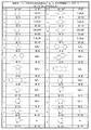
(式(1)で示される化合物の具体例)
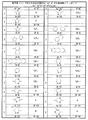
この式(1)で示される化合物の具体例としては、図1〜図4に示される、具体例<1(a)>〜<4>があげられる。図1(a)〜(f)には、nが2又は3であって、Ar1=Ar2、かつ、R1=R2の場合の具体例を示した。また、図2(a)〜(b)には、nが2又は3であって、Ar1、Ar2、R1及びR2の全てが異なる場合、Ar1とAr2とが異なり、R1及びR2は同一である場合、Ar1及びAr2は同一で、R1とR2とは異なる場合のいずれかの場合の具体例を示した。なお、図1〜図4における「Me−」はメチル基であることを示す。
(Specific examples of the compound represented by the formula (1))
Specific examples of the compound represented by the formula (1) include specific examples <1 (a)> to <4> shown in FIGS. 1A to 1F show specific examples in the case where n is 2 or 3, Ar 1 = Ar 2 , and R 1 = R 2 . 2 (a) to 2 (b), when n is 2 or 3 and all of Ar 1 , Ar 2 , R 1 and R 2 are different, Ar 1 and Ar 2 are different from each other, R In the case where 1 and R 2 are the same, Ar 1 and Ar 2 are the same, and specific examples in any case where R 1 and R 2 are different are shown. In FIG. 1 to FIG. 4, “Me-” represents a methyl group.
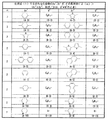
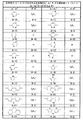
さらに、図3(a)〜(c)及び図4は、式(1)のnが2の場合であって、2つのフェニル基同士が、置換基を介して5員環又は6員環を新たに形成するように連結された化合物の場合の例を示す。式(1)のnが2の場合であって、2つのフェニル基同士が、置換基を介して5員環又は6員環を新たに形成するように連結された化合物としては、下記に示すような式(1−1)〜(1−7)に示すような化合物があげられる(式(1−6)中の「Me」はメチル基を表す。)。そして、図3(a)〜(c)には、Ar1=Ar2、かつ、R1=R2の場合の具体例を示した。また、図4には、Ar1、Ar2、R1及びR2の全てが異なる場合、Ar1とAr2とが異なり、R1及びR2は同一である場合、Ar1及びAr2は同一で、R1とR2とは異なる場合のいずれかの場合の具体例を示した。 Further, FIGS. 3A to 3C and FIG. 4 show the case where n in the formula (1) is 2, and two phenyl groups can form a 5-membered ring or a 6-membered ring via a substituent. The example in the case of the compound connected so that it may form newly is shown. Examples of the compound in which n in formula (1) is 2 and two phenyl groups are linked to form a new 5-membered ring or 6-membered ring via a substituent are shown below. Examples thereof include compounds represented by the formulas (1-1) to (1-7) (“Me” in the formula (1-6) represents a methyl group). 3A to 3C show specific examples in the case of Ar 1 = Ar 2 and R 1 = R 2 . FIG. 4 also shows that when Ar 1 , Ar 2 , R 1 and R 2 are all different, Ar 1 and Ar 2 are different, and R 1 and R 2 are the same, Ar 1 and Ar 2 are The specific example in the case where they are the same and R 1 and R 2 are different is shown.
(式(1)で示される化合物の分子量、用途)
上記式(1)(式(1−1)〜(1−7)を含む)で表される化合物の分子量は、それぞれ、好ましくは350以上、さらに好ましくは400以上、より好ましくは500以上であり、また好ましくは5000以下、さらに好ましくは3000以下、より好ましくは2000以下、特に好ましくは1500以下である。分子量をこの範囲とすることにより、化合物が安定性を有するという特徴を発揮することができる。
(Molecular weight of compound represented by formula (1), application)
The molecular weight of the compound represented by the formula (1) (including formulas (1-1) to (1-7)) is preferably 350 or more, more preferably 400 or more, and more preferably 500 or more. Also, it is preferably 5000 or less, more preferably 3000 or less, more preferably 2000 or less, and particularly preferably 1500 or less. By setting the molecular weight within this range, a characteristic that the compound has stability can be exhibited.
上記式(1)(式(1−1)〜(1−7)を含む)で表される化合物は、トランジスタ材料として用いることができる。この上記式(1)(式(1−1)〜(1−7)を含む)で表される化合物を用いたトランジスタ材料は、高いキャリア移動度だけでなく、高い発光特性を有することから、特に発光トランジスタ材料として使用することができる。 The compound represented by the above formula (1) (including formulas (1-1) to (1-7)) can be used as a transistor material. The transistor material using the compound represented by the above formula (1) (including formulas (1-1) to (1-7)) has not only high carrier mobility but also high emission characteristics. In particular, it can be used as a light emitting transistor material.
(発光トランジスタ素子)
次に、上記式(1)(式(1−1)〜(1−7)を含む)化合物を用いた発光トランジスタ素子について説明する。
上記発光トランジスタ素子としては、図5に示すような電界効果型トランジスタ(FET)の基本構造を有する素子をあげることができる。
(Light-emitting transistor element)
Next, a light-emitting transistor element using the compound of the above formula (1) (including formulas (1-1) to (1-7)) will be described.
Examples of the light-emitting transistor element include an element having a basic structure of a field effect transistor (FET) as shown in FIG.
この発光トランジスタ素子10は、キャリアとしての正孔及び電子を輸送可能であり、正孔及び電子の再結合により発光を生じる、上記ピレン系化合物を主構成成分とする発光層1、この発光層1に正孔を注入する正孔注入電極、いわゆるソース電極2、上記発光層に電子を注入する電子注入電極、いわゆるドレイン電極3,及び上記ソース電極2及びドレイン電極3に対向し、上記発光層1内のキャリアの分布を制御する、N+シリコン基板で構成されたゲート電極4から構成される。なお、ゲート電極4は、シリコン基板の表層部に形成される不純物拡散層からなる導電層で構成してもよい。
The light-emitting
具体的には、図5に示すように、ゲート電極4の上に酸化シリコン等からなる絶縁膜5が設けられ、その上にソース電極2及びドレイン電極3が間隔を開けて設けられる。そして、このソース電極2及びドレイン電極3を覆い、かつ、両電極の間に入り込むように発光層1が設けられる。
Specifically, as shown in FIG. 5, an insulating
このとき、キャリア移動度を向上させるために、絶縁膜5形成後、又はソース電極2及びドレイン電極3の形成後、シリコン基板の処理を行うことが好ましい。シリコン基板の処理方法としては、表面処理と基板温度の制御の2種類があげられる。
At this time, in order to improve the carrier mobility, it is preferable to process the silicon substrate after forming the insulating
上記の表面処理は、絶縁膜5の形成後、又はソース電極2及びドレイン電極3の形成後、UVオゾン処理し、表面処理剤を塗布する方法である。この表面処理剤としては、HMDS(ヘキサメチルジシラザン)やOTS(オクチルトリクロロシラン)などの、通常公知の表面処理剤を使用することができる。表面処理剤を塗布後、表面処理剤の残渣を取り除き、真空下で発光層に用いる化合物を蒸着する。
The surface treatment is a method in which after the formation of the insulating
上記シリコン基板の温度制御は、絶縁膜5形成後、又はソース電極2及びドレイン電極3の形成後の基板に、真空状態で熱を加えながら温度を一定にして、発光層に用いる化合物を真空蒸着する方法である。基板の温度範囲の下限は40℃が好ましい。また、基板の温度範囲の上限は、100℃が好ましく、80℃がより好ましい。なお、上記表面処理と基板の温度の制御は、両方を行ってもよい。
The temperature of the silicon substrate is controlled by vacuum deposition of the compound used for the light-emitting layer after the insulating
上記の素子が発光トランジスタの機能を発揮するためには、上記発光層1を構成する有機蛍光体、特に主構成成分であるピレン系化合物のHOMOエネルギーレベルとLUMOエネルギーレベルとの差、キャリア移動度、又は発光効率が所定の範囲を満たすことが好ましい。なお、上記のそれぞれの特徴を有する上記ピレン系化合物を用いた場合、上記ドーパント等の副構成成分を加えることにより、それぞれの機能をより高くすることが可能となる。
In order for the element to exhibit the function of a light-emitting transistor, the difference between the HOMO energy level and the LUMO energy level of the organic phosphor constituting the light-emitting
まず、上記のHOMOエネルギーレベルとLUMOエネルギーレベルとの差は、小さいほど電子の移動がより容易となって発光及び半導体性(すなわち、一方向への電子又は正孔の導通性)が生じやすくなり、好ましい。具体的には、5eV以下がよく、3eV以下がより好ましく、2.7eV以下がさらに好ましい。なお、この差は、小さいほど好ましいので、この差の下限は、0eVである。 First, the smaller the difference between the HOMO energy level and the LUMO energy level, the more easily electrons move and light emission and semiconductivity (that is, electron or hole conductivity in one direction) are more likely to occur. ,preferable. Specifically, it is preferably 5 eV or less, more preferably 3 eV or less, and even more preferably 2.7 eV or less. In addition, since this difference is so preferable that it is small, the minimum of this difference is 0 eV.
また、上記のキャリア移動度は、大きいほど半導体性が高まり好ましい。具体的には、1.0×10⁻⁵cm2/V・s以上がよく、4.0×10−5cm2/V・s以上がより好ましく、1.0×10−4cm2/V・s以上がさらに好ましい。なお、キャリア移動度の上限は、特に限定されず、1cm2/V・s程度であれば十分である。 Further, the higher the carrier mobility is, the higher the semiconducting property is. Specifically, it is preferably 1.0 × 10 −5 cm 2 / V · s or more, more preferably 4.0 × 10 −5 cm 2 / V · s or more, and 1.0 × 10 −4 cm 2 / s. V · s or more is more preferable. Note that the upper limit of the carrier mobility is not particularly limited, and is approximately 1 cm 2 / V · s.
上記発光効率は、光子や電子を入れることによって生じる光の割合をいい、注入された光エネルギーに対する、放出された光エネルギーの割合をPL発光効率(又はPL量子効率)といい、注入された電子の個数に対する、放出された光子の個数の割合をEL発光効率(又はEL量子効率)という。 The luminous efficiency refers to the ratio of light generated by inserting photons and electrons, and the ratio of emitted light energy to injected optical energy is referred to as PL luminous efficiency (or PL quantum efficiency), and injected electrons. The ratio of the number of emitted photons to the number of photons is called EL luminous efficiency (or EL quantum efficiency).
注入され、励起された電子は、正孔と再結合することにより光を発するが、この再結合は必ずしも100%の確率で生じない。このため、上記発光層1を構成する有機化合物を比較する際、EL発光効率を対比することにより、注入された光エネルギーに対する光エネルギー放出量の割合、及び電子と正孔との再結合の割合の相乗効果を比較することができる。ところで、PL発光効率を対比することにより、注入された光エネルギーに対する光エネルギー放出量の割合を比較することができるので、PL発光効率及びEL発光効率の両方を組み合わせて対比することにより、電子と正孔との再結合の割合を比較することも可能となる。
The injected and excited electrons emit light by recombining with holes, but this recombination does not necessarily occur with a probability of 100%. For this reason, when comparing the organic compound which comprises the said
上記PL発光効率は、発光の程度が大きいほど好ましく、20%以上がよく、30%以上がより好ましい。なお、PL発光効率の上限は、100%である。 The PL luminous efficiency is preferably as the light emission level is large, preferably 20% or more, and more preferably 30% or more. Note that the upper limit of the PL luminous efficiency is 100%.
また、上記EL発光効率は、発光の程度が大きいほど好ましく、1×10⁻³%以上がよく、5×10⁻³%以上が好ましい。なお、EL発光効率の上限は、100%である。 Further, the EL luminous efficiency is preferably as the degree of light emission is larger, preferably 1 × 10 −3 % or more, and more preferably 5 × 10 −3 % or more. Note that the upper limit of the EL luminous efficiency is 100%.
上記発光トランジスタ素子10の特徴として、上記以外に、発光する光の波長があげられる。この波長は、可視光の範囲内であるが、使用する有機蛍光体、特に上記ピレン系化合物の種類によって異なる波長を有する。そして、異なる波長を有する有機蛍光体を組み合わせることにより、種々の色を発現させることができる。このため、発光する光の波長は、波長そのものが特徴を発揮することとなる。
In addition to the above, the light emitting
また、上記発光トランジスタ素子10は、発光を特徴とするので、ある程度の発光輝度を有するのがよい。この発光輝度は、人間が物を見るときに感じる物の明るさに対応する発光量をいう。この発光輝度は、フォトカウンターによる測定法において、大きいほど好ましく、1×10⁴CPS(count per sec)以上がよく、1×10⁵CPS以上が好ましく、1×10⁶CPS以上がより好ましい。
Moreover, since the light emitting
上記発光層1は、構成する有機蛍光体等を蒸着(複数種あるときは、共蒸着)することにより形成される。この発光層の膜厚は、少なくとも70nm程度あればよい。
The light-emitting
上記ソース電極2及びドレイン電極3は、正孔及び電子を上記発光層1に注入するための電極で、金(Au)、マグネシウム−金合金(MgAu)等で形成される。両者間は、0.4〜50μm等の微小間隔を開けて対向するように形成される。具体的には、例えば、図6に示すように、ソース電極2及びドレイン電極3が、それぞれ複数の櫛歯からなる櫛歯形状部2a,3aを有するように形成され、ソース電極2の櫛歯形状部2aを構成する櫛歯と、ドレイン電極3の櫛歯形状部3aを構成する櫛歯とを、所定間隔を開けて交互に配置することにより、発光トランジスタ素子10としての機能をより効率的に発揮させることができる。
The
このときのソース電極2及びドレイン電極3の間隔、すなわち、櫛歯形状部2a及び櫛
歯形状部3aの間隔は、50μm以下がよく、3μm以下が好ましく、1μm以下がより好ましい。50μmを超えると、十分な半導体性を発揮し得なくなる。
The distance between the
The interval between the tooth-shaped
上記発光トランジスタ素子10は、上記ソース電極2及びドレイン電極3に電圧を印加することにより、その内部で正孔及び電子の両方を移動させ、発光層1内で、両者を再結合させることにより、発光を生じさせることができる。このとき、発光層1を通って両電極間を移動する正孔及び電子の量は、ゲート電極4に印加される電圧に依存する。このため、ゲート電極4にかける電圧及びその変化を制御することにより、上記ソース電極2及びドレイン電極3の間の導通状態を制御することが可能となる。なお、この発光トランジスタ素子10は、P型駆動を行うので、ソース電極2に対しドレイン電極3に負の電圧が加えられ、また、ソース電極2に対してゲート電極4に負の電圧が加えられる。
The light emitting
具体的には、ゲート電極4にソース電極2に対して負の電圧を印加することにより、発光層1内の正孔がゲート電極4側に引き寄せられ、絶縁膜5の表面付近における正孔の密度が高い状態となる。ソース電極2及びドレイン電極3の間の電圧を適切にすると、ゲート電極4に与える制御電圧の大小によって、ソース電極2から発光層1に正孔が注入され、ドレイン電極3から発光層1に電子が注入される状態となる。すなわち、ソース電極2が正孔注入電極として機能し、ドレイン電極3は電子注入電極として機能する。これにより、発光層1内において、正孔及び電子の再結合が生じ、これに伴う発光が生じることとなる。この発光状態は、ゲート電極4に与えられる制御電圧を変化させることにより、オン/オフさせたり、発光強度を変えたりすることができる。
Specifically, by applying a negative voltage to the
上記の正孔及び電子の再結合が生じる理論は、次のように説明することができる。ゲート電極4にソース電極2に対して負の電圧を印加することにより、図7(a)に示すように、発光層1において、絶縁膜5の界面近くに正孔のチャネル11が形成され、そのピンチオフ点12がドレイン電極3近傍に至る。そして、ピンチオフ点12とドレイン電極3とn間に高電界が形成され、図7(b)に示すように、エネルギーバンドが大きく曲げられる。これにより、ドレイン電極3内の電子が、ドレイン電極3と発光層1との間の電位障壁を突き抜けるFN(ファウラーノルドハイム)トンネル効果が生じ、発光層1内に注入され、正孔と再結合される。
The theory that the above recombination of holes and electrons can be explained as follows. By applying a negative voltage to the
また、正孔及び電子の再結合は、上記のFNトンネル効果によるという理論以外に、次の理論による説明も可能である。すなわち、図7(c)に示すように、発光層1内の有機蛍光体のHOMOエネルギーレベルにある電子が高電界によってLUMOエネルギーレベルに励起され、この励起された電子が発光層1内の正孔と再結合する。それと共に、LUMOエネルギーレベルへの励起によって空席となったHOMOエネルギーレベルにドレイン電極3から電子が注入されて補われる。
In addition to the theory that the recombination of holes and electrons is due to the above-described FN tunnel effect, the following theory is also possible. That is, as shown in FIG. 7C, the electrons at the HOMO energy level of the organic phosphor in the
上記発光トランジスタ素子10は、基板20上に、複数個、二次元配列されることにより、表示装置21を構成することができる。この表示装置21の電気回路図を図8に示す。すなわち、この表示装置21は、前述のような発光トランジスタ素子10を、マトリクス配列された画素P11,P12,……,P21,P22,……内にそれぞれ配置し、これらの画素の発光トランジスタ素子10を選択的に発光させ、また、各画素の発光トランジスタ素子10の発光強度(輝度)を制御することによって、二次元表示を可能としたものである。基板20は、例えば、ゲート電極4を一体化したシリコン基板であってもよい。すなわち、ゲート電極4は、シリコン基板の表面にパターン形成した不純物拡散層からなる導電層により構成しておけばよい。また、基板20として、ガラス基板を用いてもよい。
A plurality of the light emitting
各発光トランジスタ素子10は、P型駆動するので、そのドレイン電極3(D)にはバ
イアス電圧Vd(<0)が与えられ、そのソース電極2(S)は接地電位(=0)とされる。ゲート電極4(G)には、各画素を選択するための選択トランジスタTsと、データ保持用のキャパシタCとが並列に接続される。
Since each light emitting
The bias voltage Vd (<0) is applied, and the source electrode 2 (S) is set to the ground potential (= 0). A selection transistor Ts for selecting each pixel and a data holding capacitor C are connected in parallel to the gate electrode 4 (G).
行方向に整列した画素P11,P12,……;P21,P22,……の選択トランジスタTsのゲートは、行ごとに共通の走査線LS1,LS2,……にそれぞれ接続されている。また、列方向に整列した画素P11,P21,……;P12,P22,……の選択トランジスタTsにおいて発光トランジスタ素子10と反対側には、列ごとに共通のデータ線LD1,LD2,……がそれぞれ接続される。
The gates of the selection transistors Ts of the pixels P11, P12,..., P21, P22,... Aligned in the row direction are connected to the common scanning lines LS1, LS2,. In addition, common data lines LD1, LD2,... For each column are provided on the side opposite to the light emitting
走査線LS1,LS2,……には、コントローラ24によって制御される走査線駆動回路22から、各行の画素P11,P12,……;P21,P22,……を循環的に順次選択(行内の複数画素の一括選択)するための走査駆動信号が与えられる。すなわち、走査線駆動回路22は、各行を順次選択行として、選択行の複数の画素の選択トランジスタTsを一括して導通させ、これにより、非選択行の複数の画素の選択トランジスタTsを一括して遮断させるための走査駆動信号を発生させることができる。
For the scanning lines LS1, LS2,..., The pixels P11, P12,...; P21, P22,. A scanning drive signal for selecting pixels at a time is provided. In other words, the scanning
一方、データ線LD1,LD2,……には、データ線駆動回路23からの信号が入力される。このデータ線駆動回路23には、画像データに対応した制御信号が、コントローラ24から入力される。データ線駆動回路23は、各行の複数の画素が走査線駆動回路22によって一括選択されるタイミングで、当該選択行の各画素の発光階調に対応した発光制御信号をデータ線LD1,LD2,……に並列に供給する。
On the other hand, signals from the data line driving
これにより、選択行の各画素においては、選択トランジスタTsを介してゲート電極4(G)に発光制御信号が与えられるから、当該画素の発光トランジスタ素子10は、発光制御信号に応じた階調で発光(または消灯)することになる。発光制御信号は、キャパシタCにおいて保持されるから、走査線駆動回路22による選択行が他の行に移った後にも、ゲート電極Gの電位が保持され、発光トランジスタ素子10の発光状態が保持される。このようにして、二次元表示が可能になる。
As a result, in each pixel in the selected row, a light emission control signal is given to the gate electrode 4 (G) via the selection transistor Ts, so that the light emitting
本発明を実施例によって更に具体的に説明するが、本発明はその要旨を超えない限り、以下の実施例の記載に限定されるものではない。 Examples The present invention will be described more specifically with reference to examples. However, the present invention is not limited to the description of the following examples unless it exceeds the gist.
(合成例1)4,4’−ビフェニリレンビス(p−ブチル)スチルベン(化合物2)の合成 Synthesis Example 1 Synthesis of 4,4′-biphenylylene bis (p-butyl) stilbene (Compound 2)
300mLの四つ口フラスコにp−ブロモベンズアルデヒド3.7g(0.02mol)、p−ブチルフェニルボロン酸 4.09g(0.023mol)、Na2CO34.88g(0.046mol)、トルエン90mL、エタノール15mL、脱塩水15mLを入れ、窒素でバブリングして系内を窒素で置換した。テトラキストリフェニルホスフィンパラジウム1.16gを加えてからオイルバス中80℃で5時間、窒素気流下で加熱撹拌を行った。放冷後、反応液に脱塩水50mLを加えて分液し、有機層を無水硫酸マグネシウムで脱水後濃縮した。カラムクロマトグラフィー(シリカゲル、ヘキサン:酢酸エチル=10:1)で混在する無機塩、パラジウム、等の目的物以外の成分を除去して黄褐色の化合物1を得た。収量4.14g、収率87%、LC純度80%であった。また、1H−NMRのデータは下記の通りである。
In a 300 mL four-necked flask, 3.7 g (0.02 mol) of p-bromobenzaldehyde, 4.09 g (0.023 mol) of p-butylphenylboronic acid, 4.88 g (0.046 mol) of Na 2 CO 3 , 90 mL of toluene Then, 15 mL of ethanol and 15 mL of demineralized water were added, and the system was replaced with nitrogen by bubbling with nitrogen. After adding 1.16 g of tetrakistriphenylphosphine palladium, the mixture was heated and stirred in an oil bath at 80 ° C. for 5 hours under a nitrogen stream. After allowing to cool, 50 mL of demineralized water was added to the reaction solution and the phases were separated, and the organic layer was dehydrated over anhydrous magnesium sulfate and concentrated. Components other than the target compound such as inorganic salt and palladium mixed together by column chromatography (silica gel, hexane: ethyl acetate = 10: 1) were removed to obtain yellowish
・1H−NMR(CDCl3、400MHz)…δ10.05(s,1H)、7.94(d,2H)、7.74(d,2H)、7.563(d,2H)、7.30(d,2H.)、2.67(d,2H)、1.65(m,2H)、1.39(m,2H)、0.95(m,3H) 1 H-NMR (CDCl 3 , 400 MHz)... Δ10.05 (s, 1H), 7.94 (d, 2H), 7.74 (d, 2H), 7.563 (d, 2H), 7. 30 (d, 2H.), 2.67 (d, 2H), 1.65 (m, 2H), 1.39 (m, 2H), 0.95 (m, 3H)
300mL四つ口フラスコに、窒素ライン接続した三方コックをつけ、化合物1を1.84g(0.077mol)とテトラエチル(4,4’−ビフェニリレンジメチレン)ビフェニルホスホネートを1.59g(0.0035mol)とDMFを150mL入れて撹拌した。ここに、NaOCH3(5mol/l)メタノール溶液2.48gをDMF12mLに溶かした溶液を滴下し、室温で一晩反応させた。これを吸引ろ過し、得られた結晶をトルエン100mLで加熱懸洗し、吸引ろ過をして、粗結晶を得た。これを200mLナスフラスコに入れて100mLメタノールで1時間懸洗し、吸引ろ過をして黄色結晶の化合物2を得た。収量1.72g、収率79%(Mw:622.88)であった。また、1H−NMRのデータは下記の通りである。
A three-way cock connected to a nitrogen line was attached to a 300 mL four-necked flask, and 1.84 g (0.077 mol) of
・1H−NMR(CDCl3、400MHz)…δ7.47(d,4H)、7.22(d,2H)、7.11(d,2H)、6.98(s,2H)、6.66(d,4H.)、2.99(s,12H)、2.96(m,1H)、2.58(m,2H)、1.32(d,6H)、1.1(d,12H) 1 H-NMR (CDCl 3 , 400 MHz) δ 7.47 (d, 4H), 7.22 (d, 2H), 7.11 (d, 2H), 6.98 (s, 2H), 6. 66 (d, 4H.), 2.99 (s, 12H), 2.96 (m, 1H), 2.58 (m, 2H), 1.32 (d, 6H), 1.1 (d, 12H)
(合成例2)(4,4’−ビフェニリレンビス(p−トリフルオロスチルベン))(化合物4)の合成 (Synthesis Example 2) Synthesis of (4,4'-biphenylylenebis (p-trifluorostilbene)) (Compound 4)
300mLの四つ口フラスコにp−ブロモベンズアルデヒド3.7g(0.02mol)、p−トリフルオロメチルフェニルボロン酸 4.37g(0.023mol)、Na2CO34.88g(0.046mol)、トルエン90mL、エタノール35mL、脱塩水15mLを入れ、窒素でバブリングして系内を窒素で置換した。テトラキストリフェニルホスフィンパラジウム1.02gを加えてからオイルバス中80℃で2.5時間、窒素気流下で加熱撹拌を行った。放冷後、反応液に脱塩水100mLを加えて分液し、有機層を無水硫酸マグネシウムで脱水後濃縮した。カラムクロマトグラフィー(シリカゲル、ヘキサン:酢酸エチル=10:1)で混在する無機塩、パラジウム、等の目的物以外の成分を除去して白色の化合物1を得た。収量4.43g、収率89%、LC純度97%であった。また、1H−NMRのデータは下記の通りである。
In a 300 mL four-necked flask, 3.7 g (0.02 mol) of p-bromobenzaldehyde, 4.37 g (0.023 mol) of p-trifluoromethylphenylboronic acid, 4.88 g (0.046 mol) of Na 2 CO 3 , Toluene 90 mL, ethanol 35 mL, and
・1H−NMR(CDCl3、400MHz)…δ10.09(s,1H)、8.00(d,2H)、7.77(d,2H)、7.75(s,4H) · 1 H-NMR (CDCl 3 , 400MHz) ... δ10.09 (s, 1H), 8.00 (d, 2H), 7.77 (d, 2H), 7.75 (s, 4H)
300mL四つ口フラスコに、窒素ライン接続した三方コックをつけ、化合物3を2.20g(0.088mol)とテトラエチル(4,4’−ビフェニリレンジメチレン)ビフェニルホスホネートを1.82g(0.0035mol)とDMFを154mLを入れて撹拌した。ここに、NaOCH3(5mol/l)メタノール溶液2.48gをDMF12mLに溶かした溶液を滴下し、室温で一晩反応させた。これを吸引ろ過し、得られた結晶をトルエン100mLで加熱懸洗し、吸引ろ過をして、粗結晶を得た。これを200mLナスフラスコに入れて60mLメタノールで1時間懸洗し、吸引ろ過をして黄色結晶の化合物4を得た。収量2.35g、収率91%(Mw622.88)であった。
A three-way cock connected to a nitrogen line was attached to a 300 mL four-necked flask, and 2.20 g (0.088 mol) of
(合成例3)4,4’−ビフェニリレンビス(p−オクチルスチルベン)(化合物5)の合成
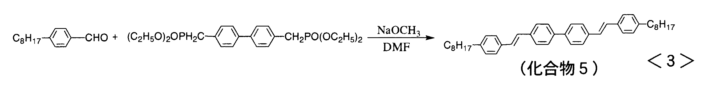
300mL四つ口フラスコに、窒素ライン接続した三方コックをつけ、p−オクチルベンズアルデヒド 1.73(0.073mol)とテトラエチル(4,4’−ビフェニリレンジメチレン)ビフェニルホスホネート1.5g(0.0033mol)とDMF120mLを入れて撹拌した。ここに、NaOCH3(5mol/lメタノール溶液)2.05gをDMF10mLに溶かした溶液を滴下し、室温で一晩反応させた。これを吸引ろ過し、得られた結晶をトルエン100mLで加熱懸洗し、吸引ろ過をして粗結晶を得た。これを200mLナスフラスコに入れて60mLメタノールで1時間懸洗し、吸引ろ過をして黄色結晶の化合物5を得た。収量2.35g、収率91%(Mw622.88)であった。
A three-way cock connected to a nitrogen line was attached to a 300 mL four-necked flask, and p-octylbenzaldehyde 1.73 (0.073 mol) and tetraethyl (4,4′-biphenylylene dimethylene) biphenylphosphonate 1.5 g (0.0033 mol) ) And 120 mL of DMF were added and stirred. A solution prepared by dissolving 2.05 g of NaOCH 3 (5 mol / l methanol solution) in 10 mL of DMF was added dropwise thereto and reacted at room temperature overnight. This was subjected to suction filtration, and the obtained crystals were heated and washed with 100 mL of toluene and subjected to suction filtration to obtain crude crystals. This was put into a 200 mL eggplant flask, washed with 60 mL methanol for 1 hour, and subjected to suction filtration to obtain yellow
(合成例4)4,4’−ビフェニリレンビス(p−ブチルスチルベン)(化合物6)の合成
300mL四つ口フラスコに、窒素ライン接続した三方コックをつけ、ブチルベンズアルデヒド1.73(0.073mol)とテトラエチル(4,4’−ビフェニリレンジメチレン)ビフェニルホスホネート1.5g(0.0033mol)とDMF120mLを入れて撹拌した。ここに、NaOCH3(5mol/lメタノール溶液)2.05gをDMF10mLに溶かした溶液を滴下し、室温で一晩反応させた。これを吸引ろ過し、得られた結晶をトルエン100mLで加熱懸洗し、吸引ろ過をして黄色結晶の化合物6を得た。収量1.25g、収率76%(Mw470.69)であった。
A 300 mL four-necked flask was fitted with a three-way cock connected to a nitrogen line, and butylbenzaldehyde 1.73 (0.073 mol) and tetraethyl (4,4′-biphenylylene dimethylene) biphenylphosphonate 1.5 g (0.0033 mol) DMF120mL was put and stirred. A solution prepared by dissolving 2.05 g of NaOCH 3 (5 mol / l methanol solution) in 10 mL of DMF was added dropwise thereto and reacted at room temperature overnight. This was subjected to suction filtration, and the resulting crystals were heated and washed with 100 mL of toluene, and suction filtered to obtain yellow
(合成例5)4,4’−ビフェニリレンビススチルベン)(化合物7)の合成
300mL四つ口フラスコに、窒素ライン接続した三方コックをつけ、ベンズアルデヒド 1.73g(0.077mol)とテトラエチル(4,4’−ビフェニリレンジメチレン)ビフェニルホスホネート1.5g(0.0035mol)とDMF120mLを入れて撹拌した。ここに、NaOCH3(5mol/lメタノール溶液)2.17gをDMF10mLに溶かした溶液を滴下し、室温で一晩反応させた。これを吸引ろ過し、得られた結晶をトルエン100mLで加熱懸洗し、吸引ろ過をして黄色結晶の化合物7を得た。収量1.11g、収率88%(Mw358.47)であった。
A 300 mL four-necked flask is equipped with a three-way cock connected to a nitrogen line, and 1.73 g (0.077 mol) of benzaldehyde, 1.5 g (0.0035 mol) of tetraethyl (4,4′-biphenylylenediethylene) biphenylphosphonate and 120 mL of DMF And stirred. A solution prepared by dissolving 2.17 g of NaOCH 3 (5 mol / l methanol solution) in 10 mL of DMF was added dropwise thereto and reacted at room temperature overnight. This was subjected to suction filtration, and the obtained crystals were heated and washed with 100 mL of toluene and suction filtered to obtain yellow crystals of
(合成例6)4,4’−ビフェニリレンビス(p−シアノスチルベン)(化合物8)の合成
200mL四つ口フラスコに、窒素ライン接続した三方コックをつけ、p−シアノベンズアルデヒド1.0g(0.076mol)とテトラエチル(4,4’−ビフェニリレンジメチレン)ビフェニルホスホネート1.58g(0.0035mol)とDMF60mLを入れて撹拌した。ここに、NaOCH3(5mol/lメタノール溶液)2.15gをDMF10mLに溶かした溶液を滴下し、室温で一晩反応させた。これを吸引ろ過し、得られた結晶をトルエン100mLで加熱懸洗し、吸引ろ過をして黄色結晶の化合物8を得た。収量1.32g、収率69%(Mw480.49)であった。
A 200 mL four-necked flask was fitted with a three-way cock connected to a nitrogen line, and 1.0 g (0.076 mol) of p-cyanobenzaldehyde and 1.58 g (0.0035 mol) of tetraethyl (4,4′-biphenylylene dimethylene) biphenylphosphonate. ) And 60 mL of DMF were added and stirred. A solution prepared by dissolving 2.15 g of NaOCH 3 (5 mol / l methanol solution) in 10 mL of DMF was added dropwise thereto and reacted at room temperature overnight. This was subjected to suction filtration, and the obtained crystals were heated and washed with 100 mL of toluene, and suction filtered to obtain yellow crystals of
(合成例7)4,4’−ビフェニリレンビス(5−オクチルチオフェニルエチニレン)(化合物10)の合成 Synthesis Example 7 Synthesis of 4,4′-biphenylylenebis (5-octylthiophenylethynylene) (Compound 10)
300mL四つ口フラスコに滴下漏斗、窒素ライン接続三方コック、低温温度計を取り付け、減圧下ヒートガンで加熱乾燥と窒素置換を繰り返し系内を窒素雰囲気とした。2−オクチルチオフェン、乾燥THF(テトラヒドロフラン)100mLを入れ、反応器を氷浴中で−5℃まで冷却した。n−ブチルリチウム(1.6Mol/l)21mLを20分かけて滴下漏斗より滴下し、滴下終了から40分水浴で25℃のまま保持しながら撹拌を継続したあと、反応気を再び氷浴中で0℃まで冷却した。乾燥DMF3.3mLをシリンジから滴下し、滴下終了から30分冷却条件下で撹拌を行ない、その後冷却用バスを外して室温に昇温し、終夜静置した。1N−HCl80mLをゆっくり加えた後トルエン100mLを加えて分液し、有機層を無水硫酸マグネシウムで脱水後濃縮し、橙色オイルを得た。溶媒(トルエン)含み収量6.44g、収率103%(Mw224.36)、HPLC純度84%であった。また、1H−NMRのデータは下記の通りである。 A 300 mL four-necked flask was equipped with a dropping funnel, a nitrogen line-connected three-way cock, and a low-temperature thermometer, and heat drying and nitrogen substitution were repeated with a heat gun under reduced pressure to create a nitrogen atmosphere in the system. 2-Octylthiophene and 100 mL of dry THF (tetrahydrofuran) were added, and the reactor was cooled to −5 ° C. in an ice bath. 21 mL of n-butyllithium (1.6 mol / l) was dropped from the dropping funnel over 20 minutes, and stirring was continued while maintaining at 25 ° C. in a water bath for 40 minutes after completion of the dropping. At 0 ° C. Dry DMF 3.3mL was dripped from the syringe, and it stirred under cooling conditions for 30 minutes after completion | finish of dripping, Then, the bath for cooling was removed, and it heated up to room temperature, and left still overnight. After slowly adding 80 mL of 1N HCl, 100 mL of toluene was added for liquid separation, and the organic layer was dehydrated with anhydrous magnesium sulfate and concentrated to obtain an orange oil. The solvent (toluene) was included, yield 6.44g, yield 103% (Mw224.36), HPLC purity 84%. The 1 H-NMR data is as follows.
・1H−NMR(CDCl3、400MHz)…δ9.81(s,1H)、7.6(d,1H)、6.89(d,1H)、2.87(m,2H)、1.71(m,2H.)、1.28(m,10H)、0.88(m,3H) · 1 H-NMR (CDCl 3 , 400MHz) ... δ9.81 (s, 1H), 7.6 (d, 1H), 6.89 (d, 1H), 2.87 (m, 2H), 1. 71 (m, 2H.), 1.28 (m, 10H), 0.88 (m, 3H)
300mL四つ口フラスコに、窒素ライン接続した三方コックをつけ、2−ホルミル−5−オクチルチオフェン(化合物9)1.18g(0.053mol)とテトラエチル(4,4’−ビフェニリレンジメチレン)ビフェニルホスホネート1.1g(0.0024mol)とDMF 95mLを入れて撹拌した。ここに、NaOCH3(5mol/lメタノール溶液)0.3gをDMF5mLに溶かした溶液を滴下し、室温で一晩反応させた。これを吸引ろ過し、得られた結晶をトルエン50mLで再結晶し、吸引ろ過をして黄色結晶の化合物10を得た。収量0.88g、収率62%(Mw594.96)、HPLC純度92%であった。また、1H−NMRのデータは下記の通りである。
A 300 mL four-necked flask was fitted with a three-way cock connected to a nitrogen line, and 1.18 g (0.053 mol) of 2-formyl-5-octylthiophene (Compound 9) and tetraethyl (4,4′-biphenylylene dimethylene) biphenyl 1.1 g (0.0024 mol) of phosphonate and 95 mL of DMF were added and stirred. A solution prepared by dissolving 0.3 g of NaOCH 3 (5 mol / l methanol solution) in 5 mL of DMF was added dropwise thereto and reacted at room temperature overnight. This was suction filtered, and the obtained crystals were recrystallized with 50 mL of toluene, and suction filtered to obtain yellow crystals of
・1H−NMR(CDCl3、400MHz)…δ7.55(d,2H)、7.50(d,2H)、7.20(d,2H)、6.88(d,2H)、6.86(s、1H)、6.67(d,2H.)、2.80(m,2H)、1.69(m,2H)、1.28(m,10H)、0.89(m,2H) 1 H-NMR (CDCl 3 , 400 MHz) δ 7.55 (d, 2H), 7.50 (d, 2H), 7.20 (d, 2H), 6.88 (d, 2H), 6. 86 (s, 1H), 6.67 (d, 2H.), 2.80 (m, 2H), 1.69 (m, 2H), 1.28 (m, 10H), 0.89 (m, 2H)
(合成例8)4,4’−ビフェニリレンビス(p−オクチルオキシスチルベン)(化合物11)の合成
滴下漏斗、窒素ライン接続三方コック、温度計、回転子を取り付けた100mL三口フラスコに4,4’−ビフェニリレンジメチレンビスホスホン酸テトラエチル(和光純薬試薬)3.01g、4−オクチルオキシベンズアルデヒド(純度90%)5.38gを入れ窒素置換した後、DMF(和光純薬試薬)50mLを加えて室温で攪拌を行った。滴下漏斗から28%ナトリウムメトキシド/メタノール溶液(和光純薬試薬)5mLを1分間で滴下し、室温で10分攪拌した後オイルバス中50℃で20時間加熱攪拌を行った。反応で析出した固体を吸引ろ過で回収し、回収固体をアセトニトリル、クロロホルム、アセトニトリルで順次洗浄し、固体を加熱減圧下で乾燥させ淡黄色粉末状固体を得た。収量3.73g、収率91.7%であった。
To a 100 mL three-necked flask equipped with a dropping funnel, a nitrogen line-connected three-way cock, a thermometer, and a rotor, 3.01 g of
(キャリア移動度、EL発光効率、PL発光効率の測定・算出)
キャリア移動度、EL発光効率、PL発光効率は以下のようにして測定・算出した。
[キャリア移動度μ(cm2/Vs)]
トランジスタ素子のドレイン電圧(Vd)とドレイン電流の関係式は次式[1]で表され、直線的に増加する(直線領域)。
(Measurement and calculation of carrier mobility, EL luminous efficiency, PL luminous efficiency)
Carrier mobility, EL luminous efficiency, and PL luminous efficiency were measured and calculated as follows.
[Carrier mobility μ (cm 2 / V s )]
The relational expression between the drain voltage (V d ) and the drain current of the transistor element is expressed by the following equation [1] and increases linearly (linear region).
また、Vdが大きくなると、チャネルのピンチ・オフによりIdは飽和して一定の値となり(飽和領域)、Idは次式[2]で表される。 Further, when V d increases, I d is saturated and becomes a constant value (saturation region) due to the pinch-off of the channel, and I d is expressed by the following equation [2].
なお、上記式[1][2]の各符号は、下記の通りである。
L :チャネル長[cm]
W :チャネル幅[cm]
Ci:ゲート絶縁膜の単位面積当たりの静電容量[F/cm2]
μsat:飽和領域における移動度[cm2/Vs]
Id:ドレイン電流[A]
Vd:ドレイン電圧[V]
Vg:ゲート電圧[V]
VT:ゲート閾値電圧[V] (これは、飽和領域におけるドレイン電圧(Vd)が一定の下でドレイン電流の1/2乗(Vdsat 1/2)をゲート電圧(Vg)に対してプロットし、漸近線が横軸と交わる点を示す。)
In addition, each code | symbol of said Formula [1] [2] is as follows.
L: Channel length [cm]
W: Channel width [cm]
C i : capacitance [F / cm 2 ] per unit area of the gate insulating film
μ sat : mobility in saturation region [cm 2 / Vs]
I d : drain current [A]
V d : drain voltage [V]
V g : gate voltage [V]
V T : gate threshold voltage [V] (this means that the drain current (V dsat 1/2 ) of the drain current is constant with respect to the gate voltage (V g ) under a constant drain voltage (V d ) in the saturation region And plot the point where the asymptote intersects the horizontal axis.)
この飽和領域におけるId 1/2とVgの関係から、トランジスタ素子中の移動度(μ)を求めることができる。 From the relationship between I d 1/2 and Vg in this saturation region, the mobility (μ) in the transistor element can be obtained.
本発明では、圧力を真空度〜5×10⁻³Pa、温度を室温とする条件の下、半導体パラメーターアナライザー(Agilent,HP4155C)を用いて、ドレイン電圧を10Vから−100Vまで、−1Vステップで、ゲート電圧を0Vから−100Vまで、−20Vステップで操作し、上式(2)を用いて移動度を算出した。 In the present invention, the drain voltage is changed from 10 V to -100 V in a -1 V step using a semiconductor parameter analyzer (Agilent, HP4155C) under conditions where the pressure is a vacuum degree to 5 × 10 -3 Pa and the temperature is room temperature. The gate voltage was operated from 0 V to −100 V in a −20 V step, and the mobility was calculated using the above equation (2).
[EL発光効率]
EL発光効率ηextは、トランジスタ素子を用いて、ドレイン電圧を10Vから−100Vまで、−1Vステップで、ゲート電圧を0Vから−100Vまで、−20Vステップで操作し、素子から発せられる発光をフォトンカウンター(Newport社製:4155C Semiconductor Parameter Analyzer)によって測定し、そこで得られた光子数[CPS]を下記式[3]を用いて光束[lw]に変換後、下記式[4]を用いてEL発光効率ηextを算出した。
[EL luminous efficiency]
The EL light emission efficiency η ext is obtained by operating the drain voltage from 10 V to −100 V in −1 V step, the gate voltage from 0 V to −100 V, and −20 V step by using a transistor element, and emitting light emitted from the element. Measured with a counter (Newport Corp .: 4155C Semiconductor Parameter Analyzer), the photon number [CPS] obtained there was converted into a luminous flux [lw] using the following formula [3], and then EL was used using the following formula [4]. Luminous efficiency η ext was calculated.
なお、上記式[3][4]の各符号は、下記の通りである。
NPC :フォトンカウンター(PC)によって観測した光子数[CPS]
XPC :光子数を光束[lw]に変換した値
r :円錐又は円の半径[cm]
h :フォトンカウンターとサンプルの距離[cm]
In addition, each code | symbol of said Formula [3] [4] is as follows.
N PC : Number of photons observed by photon counter (PC) [CPS]
X PC : Value obtained by converting the number of photons into a luminous flux [lw] r: Radius [cm] of a cone or a circle
h: Distance between photon counter and sample [cm]
(PL発光効率)
PLの発光効率は、本発明のトランジスタ材料を窒素雰囲気下において石英基板上に100nm蒸着し単層膜を形成したあと、積分球(IS−060、Labsphere Co.)を用いて、励起光として波長325nmのHe−Cdレーザ(IK5651R−G、Kimmon electric Co.)を照射し、サンプルからの発光Multi−channel photodiode(PMA−11、Hamamatsu photonics Co.)を測定することにより算出した。
(PL luminous efficiency)
The luminous efficiency of PL is determined by using a integrating sphere (IS-060, Labsphere Co.) as excitation light after forming a single layer film by depositing the transistor material of the present invention on a quartz substrate in a nitrogen atmosphere to a thickness of 100 nm. This was calculated by irradiating a 325 nm He-Cd laser (IK5651R-G, Kimoelectric Co.) and measuring light emission multi-channel photodiode (PMA-11, Hamamatsu photonics Co.) from the sample.
(実施例1)
下記の条件下、図5、図6に示す発光トランジスタ素子を製造した。
・絶縁膜5…シリコン基板上に、300nmの酸化シリコン膜を蒸着形成させ絶縁膜とした。
・ソース電極2及びドレイン電極3…それぞれ20本の櫛歯からなる櫛歯形状部を有する電極(Au、厚さ40nm)を形成し、図6に示すように、それぞれの櫛歯形状部が交互に配されるように、絶縁膜5の上に配置した。このとき、絶縁膜5と両電極との間にクロムからなる層(1nm)を設けた。また、このときのチャネル部(それぞれの櫛歯形状部間)の幅を25μm、長さを4mmとした。
・発光層1…上記製造例1で製造された化合物2からなるトランジスタ材料を、絶縁膜、ソース電極2及びドレイン電極3の周囲に覆うように蒸着することにより、発光層1を形成した。
Example 1
The light emitting transistor device shown in FIGS. 5 and 6 was manufactured under the following conditions.
Insulating film 5: A 300 nm silicon oxide film was deposited on a silicon substrate to form an insulating film.
-
得られた素子について、HOMO及びLUMOエネルギーレベル、EL発光効率、キャリア移動度を上記測定方法により測定した。また、化合物1からなるトランジスタ材料を用いて、上記測定方法により、PL発光効率を測定した。結果を表1に示す。
With respect to the obtained device, HOMO and LUMO energy levels, EL luminous efficiency, and carrier mobility were measured by the above measurement methods. Further, PL light emission efficiency was measured by the above measurement method using the transistor material composed of
(実施例2〜4)
発光層に用いる化合物として、それぞれ、上記製造例で製造された化合物5、化合物6および化合物7を用いたこと以外は、実施例1と同様にして素子を作成した。得られた素子について、HOMO及びLUMOエネルギーレベル、EL発光効率、キャリア移動度を上記測定方法により測定した。また、各化合物からなるトランジスタ材料を用いて、上記測定方法により、PL発光効率を測定した。結果を表1に示す。
本発明のトランジスタ材料はキャリア移動度が非常に高いことがわかった。
(Examples 2 to 4)
A device was prepared in the same manner as in Example 1 except that
It was found that the transistor material of the present invention has a very high carrier mobility.
(実施例5〜7)
下記操作A(HMDS処理)を行った以外は、実施例1〜4と同様にして、それぞれ素子を得た。結果を表1に示す。表面処理剤で処理することにより、キャリア移動度が向上することがわかった。
・操作A(HMDS処理):ソース電極2及びドレイン電極3を形成した後の基板を、UVオゾン処理し、表面処理剤であるHMDSを塗布して2分間置いた。その後、エアーでHMDSの残渣を取り除き、真空下で発光層に用いる化合物を蒸着した。
(Examples 5-7)
Elements were obtained in the same manner as in Examples 1 to 4, except that the following operation A (HMDS treatment) was performed. The results are shown in Table 1. It has been found that the carrier mobility is improved by the treatment with the surface treatment agent.
-Operation A (HMDS treatment): The substrate after the
(比較例1)
発光層に用いる化合物として、下記式(2)に示す比較化合物1を用いたこと以外は、実施例1〜3と同様にして素子を作成した。得られた素子について、HOMO及びLUMOエネルギーレベル、EL発光効率、キャリア移動度を上記測定方法により測定した。また、比較化合物1からなるトランジスタ材料を用いて、上記測定方法により、PL発光効率を測定した。結果を表1に示す。
(Comparative Example 1)
A device was prepared in the same manner as in Examples 1 to 3, except that
1 発光層
2 ソース電極
2a 櫛歯形状部
3 ドレイン電極
3a 櫛歯形状部
4 ゲート電極
5 絶縁膜
10 発光トランジスタ素子
11 正孔チャネル
12 ピンチオフ点
20 基板
21 表示装置
22 走査線駆動装置
23 データ線駆動装置
24 コントローラ
DESCRIPTION OF
S ソース電極
D ドレイン電極
G ゲート電極
C キャバシタ
Ts 選択トランジスタ
P11,P12 画素
LS1,LS2 走査線
LD1,LD2 データ線
S source electrode D drain electrode
G gate electrode C capacitor Ts selection transistor P11, P12 pixel LS1, LS2 scanning line LD1, LD2 data line
Claims (6)
上記芳香族炭化水素基及び芳香族複素環基は、それぞれ、上記のR1やR2以外に、置換基を有してもよいアルキル基、置換基を有してもよいアルコキシ基、置換基を有してもよい芳香族炭化水素基、置換基を有してもよい芳香族複素環基、置換基を有してもよいアリールオキシ基、置換基を有してもよいアミノ基、シアノ基、ニトロ基、ハロゲン原子を置換基として有してもよい。また、上記のアルキル基、アルコキシ基、芳香族炭化水素基、芳香族複素環基、アリールオキシ基、及びアミノ基が有してもよい置換基は、アルキル基、アルコキシ基、ハロゲン原子から選ばれる。
上記R1及びR2は、それぞれ、水素原子、置換基を有してもよいアルキル基、置換基を有してもよいアルコキシ基、置換基を有してもよいカルボキシ基、置換基を有してもよいアシル基、置換基を有してもよいスルファニル基、置換基を有してもよいシクロアルキル基、置換基を有してもよい芳香族炭化水素基、置換基を有してもよい芳香族複素環基、置換基を有してもよいアルケニル基、置換基を有してもよいアルキニル基、置換基を有してもよいアリールオキシ基、シアノ基から選ばれる基を表す。さらに、上記R1及びR2が有してもよい置換基は、アルキル基、アルコキシ基、ハロゲン原子から選ばれる。
上記のn個のベンゼン環は、それぞれ置換基を有してもよく、ベンゼン環の置換基同士が結合して環を形成していてもよい。このベンゼン環が有してもよい置換基は、アルキル基、アルコキシ基、アルキル基で置換されていてもよいアミノ基、アルケニル基、スルファニル基である。
さらに、nは、2〜6の整数を示す。) A transistor material comprising a compound represented by the following formula (1).
In addition to the above R 1 and R 2 , the aromatic hydrocarbon group and the aromatic heterocyclic group are an alkyl group that may have a substituent, an alkoxy group that may have a substituent, and a substituent. An aromatic hydrocarbon group which may have a substituent, an aromatic heterocyclic group which may have a substituent, an aryloxy group which may have a substituent, an amino group which may have a substituent, cyano You may have a group, a nitro group, and a halogen atom as a substituent. In addition, the substituent that the alkyl group, alkoxy group, aromatic hydrocarbon group, aromatic heterocyclic group, aryloxy group, and amino group may have is selected from an alkyl group, an alkoxy group, and a halogen atom. .
R 1 and R 2 each have a hydrogen atom, an alkyl group that may have a substituent, an alkoxy group that may have a substituent, a carboxy group that may have a substituent, or a substituent. An acyl group which may have a substituent, a sulfanyl group which may have a substituent, a cycloalkyl group which may have a substituent, an aromatic hydrocarbon group which may have a substituent, and a substituent Represents a group selected from an aromatic heterocyclic group which may have a substituent, an alkenyl group which may have a substituent, an alkynyl group which may have a substituent, an aryloxy group which may have a substituent, and a cyano group . Furthermore, the substituent that R 1 and R 2 may have is selected from an alkyl group, an alkoxy group, and a halogen atom.
The n benzene rings may each have a substituent, and the substituents of the benzene ring may be bonded to each other to form a ring. The substituent that the benzene ring may have is an alkyl group, an alkoxy group, an amino group that may be substituted with an alkyl group, an alkenyl group, or a sulfanyl group.
Furthermore, n shows the integer of 2-6. )
Priority Applications (1)
| Application Number | Priority Date | Filing Date | Title |
|---|---|---|---|
| JP2006077395A JP2007258253A (en) | 2006-03-20 | 2006-03-20 | Transistor material and light-emitting transistor element using the same |
Applications Claiming Priority (1)
| Application Number | Priority Date | Filing Date | Title |
|---|---|---|---|
| JP2006077395A JP2007258253A (en) | 2006-03-20 | 2006-03-20 | Transistor material and light-emitting transistor element using the same |
Publications (1)
| Publication Number | Publication Date |
|---|---|
| JP2007258253A true JP2007258253A (en) | 2007-10-04 |
Family
ID=38632219
Family Applications (1)
| Application Number | Title | Priority Date | Filing Date |
|---|---|---|---|
| JP2006077395A Pending JP2007258253A (en) | 2006-03-20 | 2006-03-20 | Transistor material and light-emitting transistor element using the same |
Country Status (1)
| Country | Link |
|---|---|
| JP (1) | JP2007258253A (en) |
Cited By (8)
| Publication number | Priority date | Publication date | Assignee | Title |
|---|---|---|---|---|
| WO2008059817A1 (en) * | 2006-11-14 | 2008-05-22 | Idemitsu Kosan Co., Ltd. | Organic thin film transistor and organic thin film light-emitting transistor |
| WO2008059816A1 (en) * | 2006-11-14 | 2008-05-22 | Idemitsu Kosan Co., Ltd. | Organic thin film transistor and organic thin film light-emitting transistor |
| WO2008062715A1 (en) * | 2006-11-24 | 2008-05-29 | Idemitsu Kosan Co., Ltd. | Organic thin film transistor and organic thin film light-emitting transistor |
| WO2008062841A1 (en) * | 2006-11-24 | 2008-05-29 | Idemitsu Kosan Co., Ltd. | Organic thin film transistor and organic thin film light-emitting transistor |
| WO2008069060A1 (en) * | 2006-12-04 | 2008-06-12 | Idemitsu Kosan Co., Ltd. | Organic thin film transistor and organic thin film light emitting transistor |
| WO2008069061A1 (en) * | 2006-12-04 | 2008-06-12 | Idemitsu Kosan Co., Ltd. | Organic thin film transistor and organic thin film light emitting transistor |
| WO2010047335A1 (en) * | 2008-10-21 | 2010-04-29 | 国立大学法人京都大学 | Benzene compound |
| JP2021527155A (en) * | 2018-06-11 | 2021-10-11 | ベーアーエスエフ エスエー | Optical data communication systems including paraphenylene vinylene and specific paraphenylene vinylene |
Citations (6)
| Publication number | Priority date | Publication date | Assignee | Title |
|---|---|---|---|---|
| JPH06271844A (en) * | 1993-03-18 | 1994-09-27 | Toyo Ink Mfg Co Ltd | Organic electroluminescent device |
| JP2001176666A (en) * | 1999-12-17 | 2001-06-29 | Matsushita Electric Ind Co Ltd | Organic electroluminescent device |
| JP2003115624A (en) * | 2001-10-05 | 2003-04-18 | Nec Corp | Organic thin film transistor |
| JP2003243411A (en) * | 2002-02-13 | 2003-08-29 | Seiko Epson Corp | Organic semiconductor device and method of manufacturing the same |
| WO2005079119A1 (en) * | 2004-02-16 | 2005-08-25 | Japan Science And Technology Agency | Light emitting transistor |
| JP2005243871A (en) * | 2004-02-26 | 2005-09-08 | Nec Corp | Organic thin film light emitting transistor and method for manufacturing the same |
-
2006
- 2006-03-20 JP JP2006077395A patent/JP2007258253A/en active Pending
Patent Citations (6)
| Publication number | Priority date | Publication date | Assignee | Title |
|---|---|---|---|---|
| JPH06271844A (en) * | 1993-03-18 | 1994-09-27 | Toyo Ink Mfg Co Ltd | Organic electroluminescent device |
| JP2001176666A (en) * | 1999-12-17 | 2001-06-29 | Matsushita Electric Ind Co Ltd | Organic electroluminescent device |
| JP2003115624A (en) * | 2001-10-05 | 2003-04-18 | Nec Corp | Organic thin film transistor |
| JP2003243411A (en) * | 2002-02-13 | 2003-08-29 | Seiko Epson Corp | Organic semiconductor device and method of manufacturing the same |
| WO2005079119A1 (en) * | 2004-02-16 | 2005-08-25 | Japan Science And Technology Agency | Light emitting transistor |
| JP2005243871A (en) * | 2004-02-26 | 2005-09-08 | Nec Corp | Organic thin film light emitting transistor and method for manufacturing the same |
Cited By (17)
| Publication number | Priority date | Publication date | Assignee | Title |
|---|---|---|---|---|
| US8022401B2 (en) | 2006-11-14 | 2011-09-20 | Idemitsu Kosan, Co., Ltd. | Organic thin film transistor and organic thin film light-emitting transistor |
| WO2008059816A1 (en) * | 2006-11-14 | 2008-05-22 | Idemitsu Kosan Co., Ltd. | Organic thin film transistor and organic thin film light-emitting transistor |
| JP5337490B2 (en) * | 2006-11-14 | 2013-11-06 | 出光興産株式会社 | Organic thin film transistor and organic thin film light emitting transistor |
| WO2008059817A1 (en) * | 2006-11-14 | 2008-05-22 | Idemitsu Kosan Co., Ltd. | Organic thin film transistor and organic thin film light-emitting transistor |
| WO2008062715A1 (en) * | 2006-11-24 | 2008-05-29 | Idemitsu Kosan Co., Ltd. | Organic thin film transistor and organic thin film light-emitting transistor |
| WO2008062841A1 (en) * | 2006-11-24 | 2008-05-29 | Idemitsu Kosan Co., Ltd. | Organic thin film transistor and organic thin film light-emitting transistor |
| JPWO2008062841A1 (en) * | 2006-11-24 | 2010-03-04 | 出光興産株式会社 | Organic thin film transistor and organic thin film light emitting transistor |
| US8203139B2 (en) | 2006-11-24 | 2012-06-19 | Idemitsu Kosan Co., Ltd | Organic thin film transistor and organic thin film light-emitting transistor using an organic semiconductor layer having an aromatic hydrocarbon group or an aromatic heterocyclic group in the center thereof |
| US8148720B2 (en) | 2006-11-24 | 2012-04-03 | Idemitsu Kosan Co., Ltd. | Organic thin film transistor and organic thin film light-emitting transistor |
| US8207525B2 (en) | 2006-12-04 | 2012-06-26 | Idemitsu Kosan Co., Ltd. | Organic thin film transistor and organic thin film light emitting transistor |
| JPWO2008069061A1 (en) * | 2006-12-04 | 2010-03-18 | 出光興産株式会社 | Organic thin film transistor and organic thin film light emitting transistor |
| WO2008069061A1 (en) * | 2006-12-04 | 2008-06-12 | Idemitsu Kosan Co., Ltd. | Organic thin film transistor and organic thin film light emitting transistor |
| US8330147B2 (en) | 2006-12-04 | 2012-12-11 | Idemitsu Kosan, Co., Ltd. | Organic thin film transistor and organic thin film light emitting transistor having organic semiconductor compound with divalent aromatic hydrocarbon group and divalent aromatic heterocyclic group |
| WO2008069060A1 (en) * | 2006-12-04 | 2008-06-12 | Idemitsu Kosan Co., Ltd. | Organic thin film transistor and organic thin film light emitting transistor |
| WO2010047335A1 (en) * | 2008-10-21 | 2010-04-29 | 国立大学法人京都大学 | Benzene compound |
| JP2021527155A (en) * | 2018-06-11 | 2021-10-11 | ベーアーエスエフ エスエー | Optical data communication systems including paraphenylene vinylene and specific paraphenylene vinylene |
| JP7212442B2 (en) | 2018-06-11 | 2023-01-25 | ベーアーエスエフ・エスエー | Optical data communication systems containing paraphenylene vinylene and certain paraphenylene vinylenes |
Similar Documents
| Publication | Publication Date | Title |
|---|---|---|
| JP5093879B2 (en) | Pyrene-based organic compounds, transistor materials, and light-emitting transistor elements | |
| US20080105865A1 (en) | Pyrene Based Compound and Light Emitting Transistor Element Using the Same | |
| EP1818322A1 (en) | Pyrene compound and, utilizing the same, light emitting transistor device and electroluminescence device | |
| Lo et al. | Sky-blue aggregation-induced emission molecules for non-doped organic light-emitting diodes | |
| Chen et al. | Naphthalimide–arylamine derivatives with aggregation induced delayed fluorescence for realizing efficient green to red electroluminescence | |
| CN106977468A (en) | Heterocyclic compounds and organic electronic devices containing them | |
| EP3266789A1 (en) | Monosubstituted diazabenzimidazole carbene metal complexes for use in organic light emitting diodes | |
| Hu et al. | Silane coupling di-carbazoles with high triplet energy as host materials for highly efficient blue phosphorescent devices | |
| Cai et al. | Sulfur-bridged tetraphenylethylene AIEgens for deep-blue organic light-emitting diodes | |
| Kang et al. | Lifetime enhancement of blue thermally activated delayed fluorescent devices by separated carrier channels using dibenzofuran-triazine type hosts | |
| Liu et al. | Pyridyl-substituted anthracene derivatives with solid-state emission and charge transport properties | |
| Lee et al. | A hole transport material with ortho-linked terphenyl core structure for high power efficiency in blue phosphorescent organic light-emitting diodes | |
| Im et al. | Effect of the molecular structure of the host materials on the lifetime of green thermally activated delayed fluorescent organic light-emitting diodes | |
| JP2007258253A (en) | Transistor material and light-emitting transistor element using the same | |
| JP2007084485A (en) | Naphthalene derivative and organic semiconductor material, and light-emitting transistor element and organic electroluminescence element using the same | |
| Yun et al. | Trisdibenzofuran-derived electron transport type exciton blocking materials for improved efficiency and lifetime in blue phosphorescent organic light-emitting diodes | |
| TW201823247A (en) | Organic compound and organic electroluminescent device using the same | |
| CN101072743A (en) | Pyrene compound, light-emitting transistor device and organic electroluminescence device using same | |
| Kim et al. | Design of bicarbazole type host materials for long-term stability in blue phosphorescent organic light-emitting diodes | |
| JP2018100264A (en) | Compound and organic electronic device using the same | |
| Park et al. | An indole derivative as a high triplet energy hole transport material for blue phosphorescent organic light-emitting diodes | |
| Gudeika et al. | High-triplet-energy derivatives of indole and carbazole as hosts for blue phosphorescent organic light-emitting diodes | |
| Kim et al. | Bicarbazole based donor–acceptor compound as a host for thermally activated delayed fluorescent emitter | |
| Kwon et al. | 4, 4′-Di (pyren-1-yl)-1, 1′-biphenyl as an efficient material for organic light-emitting diodes and thin-film transistors | |
| Bagdziunas et al. | High triplet energy exciton blocking materials based on triphenylamine core for organic light-emitting diodes |
Legal Events
| Date | Code | Title | Description |
|---|---|---|---|
| A621 | Written request for application examination |
Free format text: JAPANESE INTERMEDIATE CODE: A621 Effective date: 20071211 |
|
| A131 | Notification of reasons for refusal |
Free format text: JAPANESE INTERMEDIATE CODE: A131 Effective date: 20110412 |
|
| A02 | Decision of refusal |
Free format text: JAPANESE INTERMEDIATE CODE: A02 Effective date: 20110830 |