JP2007258281A - Flexible wiring board and connection structure thereof - Google Patents
Flexible wiring board and connection structure thereof Download PDFInfo
- Publication number
- JP2007258281A JP2007258281A JP2006077793A JP2006077793A JP2007258281A JP 2007258281 A JP2007258281 A JP 2007258281A JP 2006077793 A JP2006077793 A JP 2006077793A JP 2006077793 A JP2006077793 A JP 2006077793A JP 2007258281 A JP2007258281 A JP 2007258281A
- Authority
- JP
- Japan
- Prior art keywords
- wiring pattern
- protruding electrode
- opening
- wiring board
- flexible
- Prior art date
- Legal status (The legal status is an assumption and is not a legal conclusion. Google has not performed a legal analysis and makes no representation as to the accuracy of the status listed.)
- Pending
Links
Images





Classifications
-
- H—ELECTRICITY
- H10—SEMICONDUCTOR DEVICES; ELECTRIC SOLID-STATE DEVICES NOT OTHERWISE PROVIDED FOR
- H10W—GENERIC PACKAGES, INTERCONNECTIONS, CONNECTORS OR OTHER CONSTRUCTIONAL DETAILS OF DEVICES COVERED BY CLASS H10
- H10W74/00—Encapsulations, e.g. protective coatings
- H10W74/10—Encapsulations, e.g. protective coatings characterised by their shape or disposition
- H10W74/15—Encapsulations, e.g. protective coatings characterised by their shape or disposition on active surfaces of flip-chip devices, e.g. underfills
-
- H—ELECTRICITY
- H10—SEMICONDUCTOR DEVICES; ELECTRIC SOLID-STATE DEVICES NOT OTHERWISE PROVIDED FOR
- H10W—GENERIC PACKAGES, INTERCONNECTIONS, CONNECTORS OR OTHER CONSTRUCTIONAL DETAILS OF DEVICES COVERED BY CLASS H10
- H10W90/00—Package configurations
- H10W90/701—Package configurations characterised by the relative positions of pads or connectors relative to package parts
- H10W90/721—Package configurations characterised by the relative positions of pads or connectors relative to package parts of bump connectors
- H10W90/724—Package configurations characterised by the relative positions of pads or connectors relative to package parts of bump connectors between a chip and a stacked insulating package substrate, interposer or RDL
-
- H—ELECTRICITY
- H10—SEMICONDUCTOR DEVICES; ELECTRIC SOLID-STATE DEVICES NOT OTHERWISE PROVIDED FOR
- H10W—GENERIC PACKAGES, INTERCONNECTIONS, CONNECTORS OR OTHER CONSTRUCTIONAL DETAILS OF DEVICES COVERED BY CLASS H10
- H10W90/00—Package configurations
- H10W90/701—Package configurations characterised by the relative positions of pads or connectors relative to package parts
- H10W90/731—Package configurations characterised by the relative positions of pads or connectors relative to package parts of die-attach connectors
- H10W90/734—Package configurations characterised by the relative positions of pads or connectors relative to package parts of die-attach connectors between a chip and a stacked insulating package substrate, interposer or RDL
Landscapes
- Structures For Mounting Electric Components On Printed Circuit Boards (AREA)
- Structure Of Printed Boards (AREA)
- Wire Bonding (AREA)
Abstract
【課題】配線パターンの抵抗が低く、半導体チップと良好に電気的に接続することができるフレキシブル配線基板を実現する。
【解決手段】本発明のフレキシブル配線基板1は、フレキシブル基板2上に幅広配線パターン16が形成され、幅広配線パターン16は、開口部7を備えている。このため、フレキシブル配線基板1上に、突起電極12を備えた半導体チップ11を電気的に接続する場合、突起電極12の一部を開口部7に位置するように接続することにより、その接続状態を、開口部7を介して、フレキシブル配線基板1の裏面側から目視で確認することができる。
【選択図】図6To realize a flexible wiring board having a low resistance of a wiring pattern and capable of satisfactorily being electrically connected to a semiconductor chip.
In a flexible wiring board according to the present invention, a wide wiring pattern is formed on a flexible substrate, and the wide wiring pattern has an opening. For this reason, when electrically connecting the semiconductor chip 11 provided with the protruding electrode 12 on the flexible wiring board 1, the connection state is established by connecting a part of the protruding electrode 12 so as to be positioned in the opening 7. Can be visually confirmed through the opening 7 from the back side of the flexible wiring board 1.
[Selection] Figure 6
Description
本発明は、フレキシブル配線基板および該フレキシブル配線基板上に半導体チップを接続した接続構造に関するものである。 The present invention relates to a flexible wiring board and a connection structure in which a semiconductor chip is connected on the flexible wiring board.
現在、TVやPC用モニターを始め、携帯電話に至る様々な分野で液晶表示装置が採用されている。近年、液晶表示装置に対して、より一層の高精細および高出力化が要求されている。このため、液晶表示装置の表示機能を制御する液晶ドライバの多出力化に拍車がかかっており、用いられる半導体チップの微細化・小型化が更に進んでいる。このような流れの中で、容易に多端子を結線することができ、製品の小型化を図ることができることから、フレキシブル配線基板を用いた液晶ドライバが多く用いられている。 Currently, liquid crystal display devices are used in various fields ranging from monitors for TVs and PCs to mobile phones. In recent years, liquid crystal display devices have been required to have higher definition and higher output. For this reason, the increase in the number of outputs of the liquid crystal driver for controlling the display function of the liquid crystal display device has been spurred, and the miniaturization and miniaturization of the semiconductor chip used are further advanced. In such a flow, since it is possible to easily connect multiple terminals and to reduce the size of the product, a liquid crystal driver using a flexible wiring board is often used.
上記液晶ドライバは、フレキシブル配線基板上に設けられた配線パターン上に、ドライバチップである半導体チップを電気的に接続した構造を有している。上記半導体チップの底面には、外部出力端子として突起電極が設けられており、該突起電極と上記配線パターンとの電気的接続を介して半導体チップとフレキシブル配線基板とは接続されている。 The liquid crystal driver has a structure in which a semiconductor chip as a driver chip is electrically connected to a wiring pattern provided on a flexible wiring board. On the bottom surface of the semiconductor chip, a protruding electrode is provided as an external output terminal, and the semiconductor chip and the flexible wiring board are connected through electrical connection between the protruding electrode and the wiring pattern.
上述したように、近年、液晶ドライバが多出力化しているため、配線パターンにおける電圧は高くなり、配線パターンにかかる負荷が大きくなっている。このため、配線パターンへの負荷を極力抑制するため、配線パターンの抵抗を低くする必要がある。 As described above, in recent years, since the liquid crystal driver has increased in output, the voltage in the wiring pattern is increased and the load on the wiring pattern is increased. For this reason, in order to suppress the load on the wiring pattern as much as possible, it is necessary to reduce the resistance of the wiring pattern.
また、フレキシブル配線基板は、上記液晶ドライバのみならず、プリンタドライバとしても用いられている。プリンタドライバでは、信号源となる半導体チップと出力先であるプリンタヘッドの多端子とをフレキシブル配線基板上で結線した構成を有している。 The flexible wiring board is used not only as the liquid crystal driver but also as a printer driver. The printer driver has a configuration in which a semiconductor chip as a signal source and multiple terminals of a printer head as an output destination are connected on a flexible wiring board.
フレキシブル配線基板をプリンタドライバとして用いる場合、圧電素子であるプリンタヘッドへ電力を供給するため、液晶ドライバとして用いる場合と比べて、配線パターンにおける電圧は高い。このため、配線パターンにかかる負荷は大きく、液晶ドライバの場合と同様に、配線パターンの抵抗を低くする必要がある。 When a flexible wiring board is used as a printer driver, power is supplied to a printer head, which is a piezoelectric element, so that the voltage in the wiring pattern is higher than when the flexible wiring board is used as a liquid crystal driver. For this reason, the load applied to the wiring pattern is large, and it is necessary to reduce the resistance of the wiring pattern as in the case of the liquid crystal driver.
配線パターンの抵抗を調整する方法としては、電圧が高くなる箇所の特定の配線パターンの幅を変化させることが一般的に行われている(例えば、特許文献1参照)。 As a method for adjusting the resistance of the wiring pattern, it is common practice to change the width of a specific wiring pattern at a location where the voltage increases (see, for example, Patent Document 1).
特許文献1では、画像品位を向上させる目的で、液晶ディスプレイの引き出し配線の幅などを調整することにより、配線の抵抗を均一にすることが開示されている。
しかしながら、上記従来の構成では、抵抗を下げるために配線パターンの幅を広げると、突起電極と配線パターンとの電気的接続の信頼性が悪化するという問題を生じる。 However, in the conventional configuration, when the width of the wiring pattern is increased in order to reduce the resistance, there arises a problem that the reliability of the electrical connection between the protruding electrode and the wiring pattern is deteriorated.
具体的には、突起電極の幅よりも配線パターンの幅を広くして配線パターンの抵抗を低下させた場合、配線パターンが、配線パターンと突起電極との電気的接続部分を隠してしまうため、フレキシブル配線基板の裏面(配線パターンが形成された面とは反対側の面)側から、配線パターンと突起電極との接続状態を目視で確認することができない。このため、配線パターンと突起電極との電気的接続にバラツキが生じ易くなる。 Specifically, when the width of the wiring pattern is made wider than the width of the protruding electrode to reduce the resistance of the wiring pattern, the wiring pattern hides the electrical connection portion between the wiring pattern and the protruding electrode. The connection state between the wiring pattern and the protruding electrode cannot be visually confirmed from the back surface (surface opposite to the surface on which the wiring pattern is formed) of the flexible wiring board. For this reason, the electrical connection between the wiring pattern and the protruding electrode is likely to vary.
本発明は、上記の問題点に鑑みてなされたものであり、その目的は、配線パターンの抵抗が低く、半導体チップと良好に電気的に接続することができるフレキシブル配線基板および該フレキシブル配線基板と半導体チップとが電気的に接続した接続構造を実現することにある。 The present invention has been made in view of the above problems, and an object of the present invention is to provide a flexible wiring board that has a low resistance of a wiring pattern and can be electrically connected to a semiconductor chip well, and the flexible wiring board. The object is to realize a connection structure in which a semiconductor chip is electrically connected.
本発明に係るフレキシブル配線基板は、上記課題を解決するために、フレキシブル基板上に配線パターンが形成されたフレキシブル配線基板であって、配線パターンは、開口部を備えていることを特徴としている。 In order to solve the above problems, a flexible wiring board according to the present invention is a flexible wiring board in which a wiring pattern is formed on a flexible board, and the wiring pattern includes an opening.
上記構成によれば、配線パターンは開口部を備えているため、フレキシブル配線基板上に、突起電極を備えた半導体チップを電気的に接続する場合、突起電極の一部を上記開口部に位置するように接続することにより、配線パターンの幅を広げた場合であってもその接続状態を、配線パターンの開口部を介して、フレキシブル配線基板の裏面(配線パターンが形成された面とは反対側の面)側から目視で確認することができる。従って、上記構成によれば、配線パターンの抵抗が低く、半導体チップと良好に電気的に接続することができるフレキシブル配線基板を提供することができるという効果を奏する。 According to the above configuration, since the wiring pattern includes the opening, when a semiconductor chip including the protruding electrode is electrically connected to the flexible wiring board, a part of the protruding electrode is positioned in the opening. Even if the width of the wiring pattern is widened by connecting in this way, the connection state is changed to the back surface of the flexible wiring board (opposite to the surface on which the wiring pattern is formed) through the opening of the wiring pattern. Can be visually confirmed from the side. Therefore, according to the said structure, there exists an effect that the resistance of a wiring pattern is low and can provide the flexible wiring board which can be electrically connected with a semiconductor chip favorably.
また、突起電極を備えた半導体チップを電気的に接続する場合、突起電極の一部を上記開口部に位置するように接続することにより、突起電極は、開口部と配線パターンとの境界領域を挟み込むようにして配線パターンに接続する。このため、突起電極は、配線パターンにおける突起電極側の面(配線パターンの上面)のみならず、その側面(配線パターンの側面)とも接続することができる。よって、突起電極をフレキシブル配線基板の配線パターン上に強固に電気的に接続することができる。従って、上記構成によれば、フレキシブル配線基板上に、半導体チップを強固に電気的に接続することができる。 In addition, when electrically connecting a semiconductor chip having a protruding electrode, by connecting a part of the protruding electrode so as to be positioned in the opening, the protruding electrode has a boundary region between the opening and the wiring pattern. Connect to the wiring pattern as if sandwiched. Therefore, the protruding electrode can be connected not only to the surface on the protruding electrode side (the upper surface of the wiring pattern) but also to the side surface (side surface of the wiring pattern) of the wiring pattern. Therefore, the protruding electrode can be firmly electrically connected on the wiring pattern of the flexible wiring board. Therefore, according to the said structure, a semiconductor chip can be firmly electrically connected on a flexible wiring board.
また、突起電極が、開口部と配線パターンとの境界領域を挟み込むようにして接続するため、接続時において突起電極が受ける負荷が低減する。つまり、開口部に位置する突起電極の領域は圧縮されないため、突起電極が配線パターンの上面のみと接続する場合と比べて、突起電極が受ける負荷は全体として低減する。このため、突起電極を介してフレキシブル配線基板上に接続する半導体チップの接続時にかかる負荷を低減することができる。 Further, since the protruding electrode is connected so as to sandwich the boundary region between the opening and the wiring pattern, the load received by the protruding electrode during connection is reduced. In other words, since the region of the protruding electrode located in the opening is not compressed, the load applied to the protruding electrode is reduced as a whole compared to the case where the protruding electrode is connected only to the upper surface of the wiring pattern. For this reason, it is possible to reduce the load applied when connecting the semiconductor chip connected to the flexible wiring board via the protruding electrode.
本発明に係るフレキシブル配線基板では、上記配線パターンは、開口部を介して互いに対向する配線パターンにおける配線同士を架橋する架橋部を更に備えていることが好ましい。 In the flexible wiring board according to the present invention, it is preferable that the wiring pattern further includes a bridging portion that bridges the wirings in the wiring patterns facing each other through the opening.
上記構成によれば、配線パターンは架橋部を更に備えているため、外部接続端子として突起電極を備えた半導体チップを電気的に接続する場合、突起電極を上記架橋部に位置するように接続することにより、突起電極は、架橋部を挟み込むようにして配線パターンに接続する。突起電極は、架橋部における突起電極側の面(架橋部の上面)のみならず、その両側面(架橋部の両側面)とも電気的に接続することができるため、突起電極をフレキシブル配線基板の配線パターン上に強固に接続することができる。従って、上記構成によれば、フレキシブル配線基板上に、半導体チップを、より強固に電気的に接続することができる。 According to the above configuration, since the wiring pattern further includes a bridging portion, when electrically connecting a semiconductor chip having a protruding electrode as an external connection terminal, the protruding electrode is connected so as to be positioned at the bridging portion. Thus, the protruding electrode is connected to the wiring pattern so as to sandwich the bridging portion. Since the projecting electrode can be electrically connected not only to the surface of the bridging portion on the projecting electrode side (upper surface of the bridging portion) but also to both side surfaces (both side surfaces of the bridging portion), the projecting electrode is connected to the flexible wiring board. It can be firmly connected on the wiring pattern. Therefore, according to the said structure, a semiconductor chip can be electrically connected more firmly on a flexible wiring board.
また、突起電極が、架橋部の両側面から挟み込むようにして架橋部と接続するため、突起電極が受ける負荷はより低減する。つまり、突起電極を介してフレキシブル配線基板上に接続する半導体チップにかかる負荷をより低減することができる。 Further, since the protruding electrode is connected to the bridging portion so as to be sandwiched from both side surfaces of the bridging portion, the load received by the protruding electrode is further reduced. That is, it is possible to further reduce the load applied to the semiconductor chip connected to the flexible wiring board via the protruding electrode.
従って、上記構成によれば、半導体チップをより強固に電気的に接続することができ、半導体チップの接続時にかかる負荷をより低減することができるという更なる効果を奏する。 Therefore, according to the above configuration, the semiconductor chip can be more securely electrically connected, and a further effect that the load applied when the semiconductor chip is connected can be further reduced.
本発明に係るフレキシブル配線基板では、上記架橋部は、配線パターンと同一の材料からなることが好ましい。 In the flexible wiring board according to the present invention, the bridging portion is preferably made of the same material as the wiring pattern.
上記構成によれば、フォトエッチングなどにより、配線パターンと同様の処理によって架橋部を形成することができるため、製造工程や製造時間を増加させることなく、架橋部を設けることができる。従って、製造コストを抑制することができるという更なる効果を奏する。 According to the above configuration, since the cross-linked portion can be formed by the same process as the wiring pattern by photoetching or the like, the cross-linked portion can be provided without increasing the manufacturing process and the manufacturing time. Therefore, there is a further effect that the manufacturing cost can be suppressed.
本発明に係るフレキシブル配線基板では、上記配線パターンの開口部における側面はSnメッキされていることが好ましい。 In the flexible wiring board according to the present invention, it is preferable that the side surface of the opening of the wiring pattern is Sn-plated.
上記構成によれば、Auからなる突起電極を介して、半導体チップを接続する場合に、配線パターンの上面のみならず、開口部における配線パターンの側面においてもAu−Sn共晶合金を形成させることができるため、半導体チップをより強固に電気的に接続することができるという更なる効果を奏する。 According to the above configuration, when the semiconductor chip is connected via the protruding electrode made of Au, the Au—Sn eutectic alloy is formed not only on the upper surface of the wiring pattern but also on the side surface of the wiring pattern in the opening. Therefore, the semiconductor chip can be more securely electrically connected.
本発明に係る接続構造は、上記課題を解決するために、フレキシブル基板上に配線パターンが形成されたフレキシブル配線基板上に、突起電極を有する半導体チップが電気的に接続した接続構造であり、配線パターンは、開口部を備えており、突起電極は、開口部と配線パターンとの境界領域と電気的に接続していることを特徴としている。 In order to solve the above problems, a connection structure according to the present invention is a connection structure in which a semiconductor chip having a protruding electrode is electrically connected to a flexible wiring board having a wiring pattern formed on the flexible board. The pattern includes an opening, and the protruding electrode is electrically connected to a boundary region between the opening and the wiring pattern.
上記構成によれば、突起電極は、開口部と配線パターンとの境界領域と電気的に接続しているため、配線パターンの幅を広げた場合であってもその接続状態を、配線パターンの開口部を介して、フレキシブル配線基板の裏面(配線パターンが形成された面とは反対側の面)側から目視で確認することができる。 According to the above configuration, since the protruding electrode is electrically connected to the boundary region between the opening and the wiring pattern, even when the width of the wiring pattern is widened, the connection state is determined depending on the opening of the wiring pattern. It can visually confirm from the back surface (surface on the opposite side to the surface where the wiring pattern was formed) side of a flexible wiring board through a part.
従って、上記構成によれば、配線パターンの抵抗が低く、フレキシブル配線基板と半導体チップとが良好に電気的に接続した接続構造を提供することができるという効果を奏する。 Therefore, according to the said structure, there exists an effect that the resistance of a wiring pattern is low and can provide the connection structure where the flexible wiring board and the semiconductor chip were electrically connected favorably.
また、開口部に位置する突起電極を、開口部と配線パターンとの境界領域を挟み込むようにして配線パターンと電気的に接続させることができる。このため、突起電極は、配線パターンにおける突起電極側の面(配線パターンの上面)のみならず、その側面(配線パターンの側面)とも接続することができる。よって、突起電極と配線パターンとを強固に電気的に接続することができる。従って、半導体チップをフレキシブル配線基板上に強固に電気的に接続することができる。 Further, the protruding electrode located in the opening can be electrically connected to the wiring pattern so as to sandwich the boundary region between the opening and the wiring pattern. Therefore, the protruding electrode can be connected not only to the surface on the protruding electrode side (the upper surface of the wiring pattern) but also to the side surface (side surface of the wiring pattern) of the wiring pattern. Therefore, the protruding electrode and the wiring pattern can be firmly electrically connected. Accordingly, the semiconductor chip can be firmly electrically connected to the flexible wiring board.
本発明に係る接続構造では、上記配線パターンは、開口部を介して互いに対向する配線パターンにおける配線同士を架橋する架橋部を更に備えており、突起電極は、上記架橋部と電気的に接続していることが好ましい。 In the connection structure according to the present invention, the wiring pattern further includes a bridging portion that bridges the wirings in the wiring pattern facing each other through the opening, and the protruding electrode is electrically connected to the bridging portion. It is preferable.
上記構成によれば、配線パターンは架橋部を更に備えており、突起電極は上記架橋部と電気的に接続しているため、突起電極は、架橋部における突起電極側の面(架橋部の上面)のみならず、その両側面(架橋部の両側面)とも電気的に接続することができる。このため、突起電極は、フレキシブル配線基板とより強固に電気的に接続することができる。従って、上記構成によれば、半導体チップをフレキシブル配線基板上により強固に電気的に接続することができるという更なる効果を奏する。 According to the above configuration, since the wiring pattern further includes the bridging portion, and the protruding electrode is electrically connected to the bridging portion, the protruding electrode has a surface on the protruding electrode side (the upper surface of the bridging portion). ) As well as both side surfaces thereof (both side surfaces of the bridging portion). For this reason, the protruding electrode can be more strongly electrically connected to the flexible wiring board. Therefore, according to the said structure, there exists the further effect that a semiconductor chip can be electrically connected more firmly on a flexible wiring board.
本発明に係る接続構造では、上記突起電極と配線パターンとの接続状態を、フレキシブル配線基板における半導体チップとの接続する面の裏面側から目視で確認することができることが好ましい。 In the connection structure according to the present invention, it is preferable that the connection state between the protruding electrode and the wiring pattern can be visually confirmed from the back surface side of the surface of the flexible wiring substrate connected to the semiconductor chip.
上記構成によれば、突起電極と配線パターンとを良好に電気的に接続することができる。 According to the above configuration, the protruding electrode and the wiring pattern can be electrically connected satisfactorily.
本発明に係る接続構造では、上記架橋部の幅は、上記突起電極の幅よりも小さいことが好ましい。 In the connection structure according to the present invention, the width of the bridging portion is preferably smaller than the width of the protruding electrode.
上記構成によれば、突起電極における架橋部の両側面と接触する割合が多くなるため、突起電極は、フレキシブル配線基板とより強固に接続する。従って、上記構成によれば、フレキシブル配線基板上に、半導体チップを、より強固に電気的に接続することができるという更なる効果を奏する。 According to the above configuration, since the ratio of contact with both side surfaces of the bridging portion in the protruding electrode is increased, the protruding electrode is more firmly connected to the flexible wiring board. Therefore, according to the said structure, there exists the further effect that a semiconductor chip can be electrically connected more firmly on a flexible wiring board.
本発明に係る接続構造では、上記突起電極と上記配線パターンとは、Au−Sn共晶合金により接続していることが好ましい。 In the connection structure according to the present invention, it is preferable that the protruding electrode and the wiring pattern are connected by an Au—Sn eutectic alloy.
上記構成によれば、インナーリードボンディング(ILB)などに一般的に使用されているAu−Sn共晶合金により接続構造を形成することができるため、より簡便に、低コストで接続構造を形成することができるという更なる効果を奏する。 According to the above configuration, since the connection structure can be formed by an Au—Sn eutectic alloy generally used for inner lead bonding (ILB) or the like, the connection structure can be formed more simply and at low cost. There is a further effect that it is possible.
本発明に係る接続構造では、上記突起電極は、上記配線パターンの開口部における側面と電気的に接続していることが好ましい。 In the connection structure according to the present invention, it is preferable that the protruding electrode is electrically connected to a side surface of the opening of the wiring pattern.
上記構成によれば、突起電極は、フレキシブル配線基板とより強固に電気的に接続することができるため、フレキシブル配線基板上に、半導体チップを、より強固に電気的に接続することができる。 According to the above configuration, since the protruding electrode can be more strongly electrically connected to the flexible wiring board, the semiconductor chip can be more strongly electrically connected to the flexible wiring board.
本発明に係る接続構造では、上記架橋部は、フレキシブル基板に埋没していることが好ましい。 In the connection structure according to the present invention, it is preferable that the bridging portion is buried in a flexible substrate.
上記構成によれば、架橋部との接続により突起電極が受ける負荷が緩和されるため、突起電極を介してフレキシブル配線基板上に半導体チップを接続する際における半導体チップにかかる負荷をより低減することができるという更なる効果を奏する。 According to the above configuration, since the load received by the protruding electrode due to the connection with the bridging portion is reduced, the load applied to the semiconductor chip when the semiconductor chip is connected to the flexible wiring substrate via the protruding electrode can be further reduced. There is a further effect of being able to.
本発明に係るフレキシブル配線基板は、以上のように、フレキシブル基板上に配線パターンが形成されたフレキシブル配線基板であって、配線パターンは、開口部を備えていることを特徴としている。 As described above, the flexible wiring board according to the present invention is a flexible wiring board in which a wiring pattern is formed on the flexible board, and the wiring pattern includes an opening.
このため、配線パターンの抵抗が低く、半導体チップと良好に電気的に接続することができるフレキシブル配線基板を提供することができるという効果を奏する。 For this reason, there exists an effect that the resistance of a wiring pattern is low and the flexible wiring board which can be electrically connected with a semiconductor chip favorably can be provided.
また、本発明に係る接続構造は、以上のように、フレキシブル基板上に配線パターンが形成されたフレキシブル配線基板上に、突起電極を有する半導体チップが電気的に接続した接続構造であり、配線パターンは、開口部を備えており、突起電極は、開口部と配線パターンとの境界領域と電気的に接続していることを特徴としている。 In addition, the connection structure according to the present invention is a connection structure in which a semiconductor chip having a protruding electrode is electrically connected to a flexible wiring board having a wiring pattern formed on the flexible board as described above. Is provided with an opening, and the protruding electrode is electrically connected to a boundary region between the opening and the wiring pattern.
このため、配線パターンの抵抗が低く、半導体チップと良好に電気的に接続した接続構造を提供することができるという効果を奏する。 For this reason, there is an effect that it is possible to provide a connection structure in which the resistance of the wiring pattern is low and the semiconductor chip is electrically connected well.
〔実施の形態1〕
本発明の一実施形態について図1〜図9に基づいて説明すると以下の通りである。
[Embodiment 1]
An embodiment of the present invention will be described below with reference to FIGS.
図1は、本実施の形態に係るフレキシブル配線基板の概略構成を示す斜視図である。また、図2は、図1におけるデバイスホールの概略構成を示す平面図である。また、図3は、図2における開口部の概略構成を示す平面図である。 FIG. 1 is a perspective view showing a schematic configuration of a flexible wiring board according to the present embodiment. FIG. 2 is a plan view showing a schematic configuration of the device hole in FIG. FIG. 3 is a plan view showing a schematic configuration of the opening in FIG.
図1に示すように、本実施の形態に係るフレキシブル配線基板1は、フレキシブル基板2上に配線パターン6が形成されている。上記フレキシブル配線基板1では、配線パターン6を外部環境から保護するため、他の電子部品との接続を成す電極や端子(例えば、入力アウターリード9、出力アウターリード10、インナーリード4(図2参照))以外の配線パターン6の領域は、ソルダーレジスト3で覆われている。このため、フレキシブル配線基板1の中央部では、半導体チップとの接続端子であるインナーリード4(図2参照)を露出させるため、ソルダーレジスト3は開口され、デバイスホール5が形成されている。また、フレキシブル配線基板1の端部では、入力アウターリード9がソルダーレジスト3から露出して設けられ、入力アウターリード9が設けられた端部と対向する端部には、出力アウターリード10がソルダーレジスト3から露出して設けられている。
As shown in FIG. 1, a
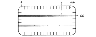
図2に示すように、デバイスホール5では、デバイスホール5を横切るようにして、幅広配線パターン(配線パターン)16が設けられ、幅広配線パターン16とソルダーレジスト3との境界付近からデバイスホール5の内側に向かってインナーリード4が露出して設けられている。
As shown in FIG. 2, in the
上記幅広配線パターン16には、開口部7が設けられており、また、図3に示すように、開口部7を介して互いに対向する配線パターンにおける幅広配線パターン16同士を架橋する架橋部8が設けられている。本実施の形態では、幅広配線パターン16は開口部7を備えているため、幅広配線パターン16の抵抗を高めることなく、フレキシブル配線基板1上に半導体チップを良好に電気的に接続することができる。以下、図4〜9を用いて、Au−Sn共晶合金接続により、フレキシブル配線基板1上に半導体チップを電気的に接続した構造(以下、接続構造と記す)について詳細に説明する。
The
尚、開口部7は、フレキシブル基板2は貫通せず、配線パターン6(幅広配線パターン16)のみを貫通して形成されている。つまり、配線パターン6(幅広配線パターン16)のみを開口して設けられている。また、言い換えれば、開口部7とは、フレキシブル基板2上における配線パターン6を構成する配線によって囲まれた領域のことである。
The
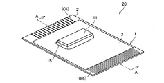
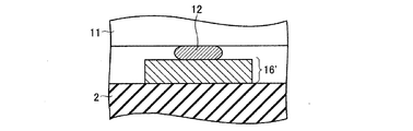
図4は、本実施の形態に係る接続構造の概略構成を示す斜視図であり、図5は、図4におけるA−A’線矢視断面図であり、図6は、図4の接続構造における幅広配線パターン16と突起電極との接続状態を示す断面図である。また、図7は、幅広配線パターン16に開口部を設けない場合における幅広パターンと突起電極との接続状態を示す断面図である。また、図8は、フレキシブル配線基板1の裏面側から見た場合の図4の接続構造における開口部7の概略構成を示す平面図であり、図9は、図8におけるB−B’線矢視断面図である。
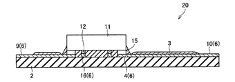
4 is a perspective view showing a schematic configuration of the connection structure according to the present embodiment, FIG. 5 is a cross-sectional view taken along line AA ′ in FIG. 4, and FIG. 6 is the connection structure of FIG. It is sectional drawing which shows the connection state of the
図4に示すように、本実施の形態に係る接続構造20は、フレキシブル配線基板1上に半導体チップ11が搭載された構造を有する。半導体チップ11は、図5に示すように、その底面に突起電極12を備えており、突起電極12と幅広配線パターン16との接続を介してフレキシブル配線基板1と電気的に接続している。デバイスホール5と半導体チップ11との間のソルダーレジスト3に被覆されていない領域は、樹脂15によって保護されている。
As shown in FIG. 4, the
突起電極12と幅広配線パターン16とは、Au−Sn共晶合金により電気的に接続されている。具体的には、Snメッキを施した幅広配線パターン16上に、金(Au)からなる突起電極12を熱圧着することにより、Au−Sn共晶合金を形成し、突起電極12と幅広配線パターン16とを電気的に接続している。
The protruding
本実施の形態に係る接続構造20は、例えば、フレキシブル配線基板1上の配線パターン6(インナーリード4および幅広配線パターン16)と半導体チップ11とをAu−Sn共晶合金により電気的に接続し、ソルダーレジスト3が被覆していないデバイスホール5(図1参照)における配線パターン6(インナーリード4および幅広配線パターン16)の領域に、樹脂15を塗布し、キュアにて樹脂15を硬化させることにより作製することができる。尚、半導体チップ11とインナーリード4との接続と同時に、半導体チップ11と幅広配線パターン16との接続を行ってもよいし、それぞれ別々に行ってもよい。
In the
本実施の形態に係る接続構造20では、幅広配線パターン16が開口部7を備えているため、図6に示すように、突起電極12の一部を開口部7上に位置するように接続することにより、開口部7上に突起電極12の一部が露出する。このため、幅広配線パターン16と突起電極12との接続状態を、フレキシブル配線基板1の裏面(幅広配線パターン16が形成された面とは反対側の面)側から目視で確認することができる。具体的には、図8に示すように、突起電極12の一部が開口部7に露出するため、突起電極12の先端(トップ面)と幅広配線パターン16の上面(突起電極12側の面)および側面との間に形成したAu−Sn共晶合金13の状態を目視で確認することができる。また、露出した突起電極12の形状を目視で観察することによって、突起電極12が幅広配線パターン16に接触している度合いについて目視で確認することができる。
In the
特に、本実施の形態のようにAu−Sn共晶合金接続により、半導体チップ11と幅広配線パターン16とを電気的に接続する場合では、(a)Au−Sn共晶合金の状態、および(b)半導体チップ11の突起電極12と幅広配線パターン16との食い込み量(突起電極12における幅広配線パターン16の側面との接触した面積の割合)が重要な評価項目となる。このため、幅広配線パターン16が開口部7を有していないため、幅広配線パターン16と突起電極12との接続状態を目視で確認することができない従来技術の構成と比べて、本実施の形態の接続構造20では、上述したように、(a)Au−Sn共晶合金の状態、および(b)半導体チップ11の突起電極12と幅広配線パターン16との食い込み量、つまり、突起電極12が幅広配線パターン16に接触している度合いについて目視で確認することができる。このため、幅広配線パターン16の抵抗を高めることなく、半導体チップ11と幅広配線パターン16とを良好に電気的に接続させることができる。
In particular, when the
また、突起電極12の一部を上記開口部7に位置するように接触させることにより、開口部7に位置する突起電極12を、図6に示すように、開口部7と架橋部8(幅広配線パターン16)との境界領域を挟み込むようにして架橋部8と電気的に接続させることができる。突起電極12は、架橋部8における突起電極12側の面(架橋部8の上面)のみならず、その側面(架橋部8の側面)とも接続することができるため、突起電極12は、アンカー効果により、架橋部8と強固に電気的に接続することができる。従って、本実施の形態に係るフレキシブル配線基板1を用いることで、フレキシブル配線基板1上に、半導体チップ11を、強固に電気的に接続することができる。
Further, by contacting a part of the protruding
更には、突起電極12が、開口部7と架橋部8(幅広配線パターン16)との境界領域を挟み込むようにして接続するため、突起電極12が受ける負荷が低減する。つまり、突起電極12と架橋部8との接続時に、開口部7に位置する突起電極12の領域は圧縮されないため、突起電極12が架橋部8の上面のみと電気的に接続する場合と比べて、突起電極12が受ける負荷は全体として低減する。このため、突起電極12を介してフレキシブル配線基板1上に接続する半導体チップ11にかかる負荷は低減する。
Furthermore, since the protruding
言い換えれば、開口部7と架橋部8(幅広配線パターン16)との境界領域を挟み込むようにして成される突起電極12と架橋部8との接続は、半導体チップ11を架橋部8に接続する際に、半導体チップ11にかかる圧力を緩衝するように作用する。このため、半導体チップ11のパッド下積層構造へのダメージを抑制することができる。
In other words, the connection between the protruding
また、半導体チップ11を、幅広配線パターン16およびインナーリード4と一括で接続する場合、Snメッキの供給量をインナーリード4に合わせると、幅広配線パターン16では配線の幅が広いためSnが過剰にメッキされ易くなり、Au−Sn共晶合金が過剰に形成される。また、Snメッキの厚さや接続温度などが過剰な接続条件となった場合にも、形成されるAu−Sn共晶合金の量が過多となる。このような場合では、半導体チップ11の保護膜が不十分であると、液相のAu−Sn共晶合金が半導体チップ11の表面に流れ、ショート不良を引き起こす不具合が生じる。しかしながら、本実施の形態に係るフレキシブル配線基板1では、幅広配線パターン16に開口部7を設けているため、過剰の液相のAu−Sn共晶合金は、半導体チップ11の表面には流れて行かず、開口部7の側面に広がる。従って、本実施の形態に係る接続構造20では、半導体チップ11のショート不良などの不具合を抑制することができる。
Further, when the
図7に示すように、従来の幅広配線パターン16’を設けたフレキシブル配線基板上では、突起電極12を備えた半導体チップ11を電気的に接続する場合、突起電極12が幅広配線パターン16’によって隠れてしまうため、フレキシブル配線基板1の裏面側から、突起電極12の先端(トップ面)と幅広配線パターン16’の上面(突起電極12側の面)との間に形成したAu−Sn共晶合金の状態を目視で確認することができない。また、幅広配線パターン16’には開口部がないため、突起電極12は幅広配線パターン16’の上面とのみ接触して接続する。このため、フレキシブル配線基板と半導体チップ11との接続強度は不十分である。更には、突起電極12は幅広配線パターン16’の上面とのみ接触して接続するため、接続時における半導体チップ11にかかる負荷は大きく、接続時に半導体チップ11が破壊する恐れがある。
As shown in FIG. 7, on the flexible wiring board provided with the conventional
本実施の形態に係るフレキシブル配線基板1におけるフレキシブル基板2の材質としては、裏面側から開口部7を介して突起電極12を目視により確認できれば特には限定されず、従来公知の材料を用いることができる。具体的には、ポリイミド、ポリエステルなどが挙げられ、加工性、耐熱性、耐溶剤性および絶縁性に優れているため、ポリイミドがより好ましい。また、フレキシブル基板2の厚さは特には限定されず、例えば47μmtとすることができる。
The material of the
フレキシブル配線基板1の裏面側から、フレキシブル基板2を透過して、Au−Sn共晶合金の状態の確認を良好に行うことができるため、カプトン(登録商標)EN(東レデュポン製)を採用した、(株)住友金属鉱山社製の商品名「エスパーフレックス」を用いることがより好ましい。
Kapton (registered trademark) EN (manufactured by Toray DuPont) was adopted because the state of the Au—Sn eutectic alloy can be satisfactorily confirmed through the
幅広配線パターン16などの配線パターン6の材質としては、特には限定されず、従来公知の材料を用いることができる。具体的には、銅(Cu)などが挙げられる。配線パターン6の厚さは、特には限定されず、例えば8μmtに設定される。配線パターン6は、例えば、電解メッキなどにより形成することができる。また、配線パターン6の材質が銅(Cu)である場合、フレキシブル基板2と配線パターン6との間に、銅(Cu)の電解メッキのため、NiCr合金層(例えば、厚さ30nm)を設けてもかまわない。
The material of the
幅広配線パターン16の幅は、フレキシブル基板2の種類や、取り扱う電流の大きさなどにより適宜選択され、例えば、フレキシブル基板2として、厚さが8μmtのCuパターンを有する(株)住友金属鉱山社製の商品名「エスパーフレックス」を用い、約1Aの電流を扱う場合では、200μmに設定することができる。
Width of the
開口部7の形状は、幅広配線パターン16と突起電極12との接続状態が目視で確認できれば特には限定されず、円形であっても多角形であってもかまわない。また多角形である場合、角が丸まっていても(角にRを有していても)かまわない。更には、接続される突起電極12一箇所あたりの開口部7は何箇所であってもかまわない。
The shape of the
開口部7の幅w(架橋部8を取り除いた場合における開口部7の中心を通る一端から他端までの距離)は特には限定されないが、図8に示すように、架橋部8を備えている場合では、接続した突起電極12の幅f(開口部7の開口面と平行な方向における突起電極12の中心を通る一端から他端までの距離)よりも大きいことが好ましい。接続する突起電極12の幅fよりも開口部7の幅wが大きいことにより、架橋部8によって遮蔽される部分以外の突起電極12の部分を、開口部7から完全に露出させることができる。このため、幅広配線パターン16と突起電極12との接続状態の目視による確認を良好に行うことができる。
The width w of the opening 7 (the distance from one end to the other end passing through the center of the
架橋部8の材質としては、特には限定されず、幅広配線パターン16に用いられる上述した従来公知の材料を用いることができる。また、幅広配線パターン16と架橋部8とは材質が同じであってもよく、異なっていてもよい。
The material of the bridging
但し、幅広配線パターン16と架橋部8との材質が同じである場合には、上記架橋部8は幅広配線パターン16と一体化することになる。つまり、2つの開口部7を近接して設けることにより架橋部8を形成することができるため、通常のフレキシブル配線基板の製造工程(テープ作製工程)で用いられる配線パターンのフォトエッチング工程により架橋部8を形成することができる。従って、製造工程や製造時間を増加させることなく、架橋部を設けることができるため、製造コストを抑制することができる。
However, when the
架橋部8の幅d(架橋する方向に対して直行する方向における幅)は、図8に示すように、開口部7から突起電極12が露出するように、突起電極12の幅fよりも小さければ特には限定されず、例えば、突起電極12の幅fの1/4以上1/2以下の範囲内に設定することができる。また、架橋部8は厚さ方向(架橋部8の幅dの方向および架橋部8の架橋する方向に対して垂直の方向)における幅k(図6参照)が均一である必要はなく、例えば、フレキシブル基板2と接する面から架橋部8の表面側に向かって幅を狭くして、架橋部8の形状を断面が三角形となるような形状としてもかまわない。架橋部8をこのような形状にすることによって、架橋部8の強度を低下させることなく、突起電極12と架橋部8の側面との接触面積を最大化させることができる。従って、突起電極12を幅広配線パターン16とより強固に接続させることが可能となる。
The width d of the bridging portion 8 (width in a direction perpendicular to the bridging direction) should be smaller than the width f of the
尚、本実施の形態では、開口部7は、縦100μm横60μmの4つの角が丸まった長方形であり、幅20μmの架橋部8によって、縦100μm横20μmの大きさが同じ2つの長方形に分断するように架橋されている。
In the present embodiment, the
突起電極12の材質は、特には限定されず、従来公知の材料を用いることができる。具体的にはハンダや金(Au)などが挙げられる。突起電極12の材質が、本実施の形態のように金(Au)である場合、突起電極12は幅広配線パターン16とAu−Sn共晶合金接続により電気的に接続することができ、この場合には、幅広配線パターン16の表面はSnメッキされる。
The material of the protruding
突起電極12の材質が本実施の形態のように金(Au)である場合、架橋部8(幅広配線パターン16)の開口部7における側面はSnメッキされていることが好ましい。これにより、フレキシブル配線基板1と半導体チップ11とを接続する場合に、架橋部8(幅広配線パターン16)の上面のみならず、架橋部8の側面においてもAu−Sn共晶合金を形成させることができるため、半導体チップ11をより強固に電気的に接続することができる。
When the material of the protruding
本実施の形態に係る接続構造20では、図9に示すように、架橋部8は、突起電極12との接続前と比べて長さ(架橋方向における幅)が伸びていることが好ましい。言い換えれば、上記架橋部8は、フレキシブル基板2側に埋没していることが好ましい。これにより、架橋部8との接続により突起電極12が受ける負荷が緩和されるため、突起電極12を介してフレキシブル配線基板1上に接続する半導体チップ11にかかる負荷をより低減することができる。
In the
上記架橋部8のフレキシブル基板2側への埋没量は、突起電極12と架橋部8(幅広配線パターン16)との食い込み量(突起電極12における架橋部8の側面との接触した面積の割合)を制御することにより、調整することができる。例えば、320〜380℃の範囲内のボンディング温度で、0.0025〜0.0075g/μm2の範囲内のボンディング圧力で、0.3〜0.5秒の範囲内のボンディング時間の範囲内の条件で、突起電極12と架橋部8とを接続することにより、架橋部8を、フレキシブル基板2側へ1〜2μmの範囲内で埋没させることができる。
The amount of the bridging
本実施の形態に係る接続構造20は、例えば、出力アウターリード10を液晶パネル(図示せず)などのフラットパネルディスプレイ(以下、FPDと記す)に電気的に接続することにより、FPD用ドライバとして用いることができる。
The
このようなフレキシブル配線基板1を用いたFPD用ドライバは、(1)金(Au)突起電極を有する半導体チップ11を、配線にSnメッキしたフレキシブル配線基板1上に電気的に接続することにより、Au−Sn共晶合金接続によって全端子の一括接続を行うことが可能である、(2)FPD用ドライバより信号を受けるFPDの電極が櫛歯のように多数の電極が同一方向に延長されたFPDと同様に、櫛歯状の電極からなる出力端子を有しているため、ACF(異方性導電フィルム)によりFPDへの一括接続が可能である、(3)一般的なフォトエッチング工程により、半導体チップ11から出力アウターリード10までの配線を作製することができる、(4)FPD用ドライバをFPDに電気的に接続後、FPD用ドライバを構成するフレキシブル配線基板1を、FPDにおけるパネルエッジを基点に折り曲げることにより、ほぼ接続前のFPDの大きさを維持できる、などの有利な点を有している。つまり、フレキシブル配線基板1をFPD用ドライバとして用いる有利な点は、好適に多端子を結線することができ、FPDを小型化することができることである。これらのことに加えて、本実施の形態に係る接続構造20では、幅広配線パターン16が開口部7を有しているため、使用電圧を高めた場合であっても、幅広配線パターン16の抵抗を高めることなく、半導体チップ11との良好な電気的接続を確保することができる。
An FPD driver using such a flexible wiring board 1 (1) electrically connects a
尚、上述の説明では、幅広配線パターン16が架橋部8を備えた構成について説明したが、これに限るものではない。架橋部8を備えていなくてもよい。幅広配線パターン16が開口部7を備えていれば、本実施形態と略同様の効果が得られる。この場合、突起電極12のが配線パターンにおける開口部との境界領域と電気的に接続することにより(つまり、突起電極12の一部を上記開口部7に位置するように接続することにより)、その接続状態を、架橋部8を備えた場合と同様に、開口部7を介して、フレキシブル配線基板1の裏面側から目視で確認することができる。
In the above description, the configuration in which the
また、突起電極12を備えた半導体チップ11を電気的に接続する場合、突起電極12の一部を上記開口部7に位置するように接続することにより、開口部7に位置する突起電極12を、開口部7と幅広配線パターン16との境界領域を挟み込むようにして幅広配線パターン16に接続することができる。突起電極12は、幅広配線パターン16における突起電極12側の面(幅広配線パターン16の上面)のみならず、その側面(幅広配線パターン16の側面)とも接続することができるため、突起電極12をフレキシブル配線基板1の幅広配線パターン16上に強固に接続することができる。従って、フレキシブル配線基板1上に、半導体チップ11を、強固に電気的に接続することができる。
When electrically connecting the
更には、突起電極12を備えた半導体チップ11を電気的に接続する場合、架橋部8を備えた場合と同様に、突起電極12の一部を上記開口部7に位置するように接続することにより、開口部7に位置する突起電極12は、開口部7と幅広配線パターン16との境界領域を挟み込むようにして幅広配線パターン16と接続する。このため、突起電極12が幅広配線パターン16の上面のみと接続する場合と比べて、開口部7に位置する突起電極12の領域は圧縮されないため、突起電極12が受ける負荷は全体として低減する。
Furthermore, when electrically connecting the
但し、本実施形態のように、開口部7に架橋部8が設けられている構成では、突起電極12は、架橋部8における突起電極12側の面(架橋部8の上面)のみならず、その両側面(架橋部8の両側面)と接続することができるため、架橋部8を設けない場合と比較して、突起電極12は、幅広配線パターン16とより強固に接続することができる。また、突起電極12が、架橋部8の両側面から挟み込むようにして架橋部8と接続するため、突起電極12が受ける負荷はより低減される。つまり、突起電極12を介してフレキシブル配線基板1上に接続する半導体チップ11にかかる負荷をより低減することができる。
However, in the configuration in which the bridging
また、架橋部8を備えない場合であっても、例えば、開口部7がコ字型(開口部7を架橋せずに、一方の端部のみから開口部7の中心に突き出た形状)のような形状を有していれば、架橋部8を有している場合と略同様の効果を奏する。
Further, even when the
また、上述の説明では、開口部7一箇所あたりに架橋部8を一つ設けた場合について説明したが、これに限るものではない。開口部7一箇所あたり二つ以上の架橋部8を設けていてもよい。開口部7一箇所あたり二つ以上の架橋部8を設けていても本実施形態と略同様の効果が得られる。
In the above description, the case where one
また、上述の説明では、半導体チップ11とフレキシブル配線基板1とをAu−Sn共晶合金接続により電気的に接続した場合について説明したが、これに限るものではない。ハンダによる接続であってもよい。突起電極12が幅広配線パターン16と電気的に接続することができる構成であれば、本実施形態と略同様の効果が得られる。
In the above description, the case where the
但し、半導体チップ11とフレキシブル配線基板1とをAu−Sn共晶合金接続により接続した場合では、インナーリードボンディングで一般的に用いる材料と同じ材料を用いることができ、Snメッキなどを一括で形成させることができる。また、その接続も一括で行うことができる。このため、特殊な工程が不要で、従来から用いられている材料およびプロセスを適用することにより電気的に接続を行うことができる。
However, when the
〔実施の形態2〕
本発明の一実施形態について図10および図11に基づいて説明すると以下の通りである。但し、上述した実施の形態1における部材と同一の部材には同一の符号を付し、その説明は省略する。実施の形態1において、出力アウターリード10の代わりにプリンタヘッドを設けていること以外は、実施の形態1の構成と同じ構成で、接続構造が形成されている。
[Embodiment 2]
One embodiment of the present invention is described below with reference to FIGS. 10 and 11. However, the same members as those in the first embodiment described above are denoted by the same reference numerals, and the description thereof is omitted. In the first embodiment, a connection structure is formed with the same configuration as that of the first embodiment except that a printer head is provided instead of the output
図10は、本実施の形態に係る接続構造の概略構成を示す斜視図である。また、図11は、図10におけるC−C’線矢視断面図である。 FIG. 10 is a perspective view showing a schematic configuration of the connection structure according to the present embodiment. FIG. 11 is a cross-sectional view taken along line C-C ′ in FIG. 10.
図10に示すように、本実施の形態に係る接続構造40は、接続構造20における出力アウターリード10の代わりにプリンタヘッド50を備えている。プリンタヘッド50は、配線パターン6を介して半導体チップ11と電気的に接続している。
As shown in FIG. 10, the
プリンタヘッド50は圧電素子であるため、取り扱う電圧が高く、配線パターン6への負荷が大きい。このため、幅広配線パターン16を用いる必要がある。本実施の形態に係る接続構造40では、実施の形態1の接続構造20と同様に、幅広配線パターン16が開口部7を備えているため、幅広配線パターン16の幅をより広くした場合であっても、半導体チップ11をフレキシブル配線基板41上に良好に電気的に接続することができる。
Since the
このようにして得られる接続構造40は、プリンタヘッド50を備えているため、プリンタドライバとして用いることができる。本実施の形態に係る接続構造40も実施の形態1における接続構造20と同様に、信号源となる半導体チップ11の多端子と出力先であるプリンタヘッド50の多端子とをフレキシブル配線基板1上で結線しているため、モジュール化に好適であり、接続構造40からなるプリンタドライバを、筐体にコンパクトに収容して組み込むことができる。
Since the
本発明に係るフレキシブル配線基板は、開口を跨ぐパターンを配線パターン内に形成していたものであってもよい。また、上記フレキシブル配線基板では、開口を跨ぐパターンの側面にSnメッキしたことが好ましい。また、上記フレキシブル配線基板では、開口を跨ぐパターンは配線パターンと同一材料で且つ一体化していることが好ましい。 The flexible wiring board according to the present invention may be one in which a pattern straddling the opening is formed in the wiring pattern. Moreover, in the said flexible wiring board, it is preferable to Sn-plat on the side surface of the pattern straddling opening. Moreover, in the said flexible wiring board, it is preferable that the pattern straddling opening is the same material and integrated with the wiring pattern.
また、本発明に係る接続構造は、上記開口を跨ぐパターンに半導体チップの突起電極を接続したものであってもよい。上記接続構造では、接続された突起電極が開口により露出されていることが好ましい。また、上記接続構造では、開口を跨ぐパターンは接続された突起電極の幅よりその幅が狭いことが好ましい。また、上記接続構造では、開口を跨ぐパターンと突起電極との接続はAu−Su共晶であることが好ましい。また、上記接続構造では、Au−Sn共晶合金接続の液相合金は開口の側面に沿って広がることが好ましい。また、上記接続構造では、開口を跨ぐパターンが突起電極への接続後、元の長さより伸びたことが好ましい。また、上記接続構造では、開口を跨ぐパターンはフレキシブル配線基板の基材に埋没することが好ましい。 Further, the connection structure according to the present invention may be one in which the protruding electrode of the semiconductor chip is connected to the pattern straddling the opening. In the above connection structure, it is preferable that the connected protruding electrode is exposed through the opening. In the above connection structure, the width of the pattern straddling the opening is preferably narrower than the width of the connected protruding electrode. In the connection structure described above, the connection between the pattern straddling the opening and the protruding electrode is preferably an Au—Su eutectic. In the above connection structure, it is preferable that the liquid phase alloy connected to the Au—Sn eutectic alloy spreads along the side surface of the opening. Moreover, in the said connection structure, it is preferable that the pattern straddling opening was extended from the original length after the connection to a protruding electrode. Moreover, in the said connection structure, it is preferable that the pattern straddling opening is embed | buried in the base material of a flexible wiring board.
本発明は上述した各実施形態に限定されるものではなく、請求項に示した範囲で種々の変更が可能であり、異なる実施形態にそれぞれ開示された技術的手段を適宜組み合わせて得られる実施形態についても本発明の技術的範囲に含まれる。 The present invention is not limited to the above-described embodiments, and various modifications are possible within the scope shown in the claims, and embodiments obtained by appropriately combining technical means disclosed in different embodiments. Is also included in the technical scope of the present invention.
本発明のフレキシブル配線基板は、配線パターンが開口部を有しているため、配線パターンの抵抗が低く、半導体チップと良好に接続することができる。このため、液晶ドライバやプリンタドライバなどに好適に用いることができる。従って、本発明のフレキシブル配線基板は、家庭から工業設備にいたる様々な電子機器または電気製品の分野に好適に用いることができる。 In the flexible wiring board of the present invention, since the wiring pattern has an opening, the resistance of the wiring pattern is low, and it can be connected to the semiconductor chip satisfactorily. Therefore, it can be suitably used for a liquid crystal driver, a printer driver, and the like. Therefore, the flexible wiring board of the present invention can be suitably used in the fields of various electronic devices or electrical products from homes to industrial facilities.
1 フレキシブル配線基板
2 フレキシブル基板
6 配線
7 開口部
8 架橋部
11 半導体チップ
12 突起電極
16 幅広配線パターン(配線)
20 接続構造
40 接続構造
41 フレキシブル配線基板
DESCRIPTION OF
20
Claims (11)
配線パターンは、開口部を備えていることを特徴とするフレキシブル配線基板。 A flexible wiring board having a wiring pattern formed on a flexible board,
A flexible wiring board, wherein the wiring pattern includes an opening.
配線パターンは、開口部を備えており、
突起電極は、配線パターンにおける開口部との境界領域と電気的に接続していることを特徴とする接続構造。 A connection structure in which a semiconductor chip having a protruding electrode is electrically connected to a flexible wiring board having a wiring pattern formed on the flexible board,
The wiring pattern has an opening,
The projecting electrode is electrically connected to a boundary region with the opening in the wiring pattern.
上記突起電極は、上記架橋部と電気的に接続していることを特徴とする請求項5に記載の接続構造。 The wiring pattern further includes a bridging portion for bridging the wirings in the wiring pattern facing each other through the opening,
The connection structure according to claim 5, wherein the protruding electrode is electrically connected to the bridging portion.
Priority Applications (1)
| Application Number | Priority Date | Filing Date | Title |
|---|---|---|---|
| JP2006077793A JP2007258281A (en) | 2006-03-20 | 2006-03-20 | Flexible wiring board and connection structure thereof |
Applications Claiming Priority (1)
| Application Number | Priority Date | Filing Date | Title |
|---|---|---|---|
| JP2006077793A JP2007258281A (en) | 2006-03-20 | 2006-03-20 | Flexible wiring board and connection structure thereof |
Publications (1)
| Publication Number | Publication Date |
|---|---|
| JP2007258281A true JP2007258281A (en) | 2007-10-04 |
Family
ID=38632240
Family Applications (1)
| Application Number | Title | Priority Date | Filing Date |
|---|---|---|---|
| JP2006077793A Pending JP2007258281A (en) | 2006-03-20 | 2006-03-20 | Flexible wiring board and connection structure thereof |
Country Status (1)
| Country | Link |
|---|---|
| JP (1) | JP2007258281A (en) |
Cited By (2)
| Publication number | Priority date | Publication date | Assignee | Title |
|---|---|---|---|---|
| JP2021027264A (en) * | 2019-08-08 | 2021-02-22 | ローム株式会社 | Semiconductor device, manufacturing method of the same, and electronic device |
| CN114096054A (en) * | 2021-11-24 | 2022-02-25 | 京东方科技集团股份有限公司 | Flexible circuit board assembly, manufacturing method thereof and display device |
Citations (5)
| Publication number | Priority date | Publication date | Assignee | Title |
|---|---|---|---|---|
| JPH11204913A (en) * | 1998-01-09 | 1999-07-30 | Sony Corp | Circuit board, mounting method, and printed wiring board |
| JP2001035880A (en) * | 1990-07-09 | 2001-02-09 | Semiconductor Energy Lab Co Ltd | Method for manufacturing display device and image sensor device |
| JP2003197812A (en) * | 2001-12-28 | 2003-07-11 | Seiko Epson Corp | Wiring board and its manufacturing method, semiconductor device and its manufacturing method, circuit board, and electronic equipment |
| JP2004356568A (en) * | 2003-05-30 | 2004-12-16 | Optrex Corp | Flexible circuit board |
| JP2005317836A (en) * | 2004-04-30 | 2005-11-10 | Nitto Denko Corp | Wiring circuit board and manufacturing method thereof |
-
2006
- 2006-03-20 JP JP2006077793A patent/JP2007258281A/en active Pending
Patent Citations (5)
| Publication number | Priority date | Publication date | Assignee | Title |
|---|---|---|---|---|
| JP2001035880A (en) * | 1990-07-09 | 2001-02-09 | Semiconductor Energy Lab Co Ltd | Method for manufacturing display device and image sensor device |
| JPH11204913A (en) * | 1998-01-09 | 1999-07-30 | Sony Corp | Circuit board, mounting method, and printed wiring board |
| JP2003197812A (en) * | 2001-12-28 | 2003-07-11 | Seiko Epson Corp | Wiring board and its manufacturing method, semiconductor device and its manufacturing method, circuit board, and electronic equipment |
| JP2004356568A (en) * | 2003-05-30 | 2004-12-16 | Optrex Corp | Flexible circuit board |
| JP2005317836A (en) * | 2004-04-30 | 2005-11-10 | Nitto Denko Corp | Wiring circuit board and manufacturing method thereof |
Cited By (3)
| Publication number | Priority date | Publication date | Assignee | Title |
|---|---|---|---|---|
| JP2021027264A (en) * | 2019-08-08 | 2021-02-22 | ローム株式会社 | Semiconductor device, manufacturing method of the same, and electronic device |
| JP7454345B2 (en) | 2019-08-08 | 2024-03-22 | ローム株式会社 | Semiconductor devices and their manufacturing methods, and electronic equipment |
| CN114096054A (en) * | 2021-11-24 | 2022-02-25 | 京东方科技集团股份有限公司 | Flexible circuit board assembly, manufacturing method thereof and display device |
Similar Documents
| Publication | Publication Date | Title |
|---|---|---|
| US6441474B2 (en) | Semiconductor device and liquid crystal module adopting the same | |
| CN101060205B (en) | Flat display panel and connection structure | |
| JP2007305881A (en) | Tape carrier, semiconductor device, and semiconductor module device | |
| JP2004193223A (en) | Semiconductor device | |
| CN101136388A (en) | Chip film package and display panel assembly having the chip film package | |
| JP5445340B2 (en) | Substrate reinforcement structure, substrate assembly, and electronic device | |
| US20010054751A1 (en) | Semiconductor device and liquid crystal module | |
| JP4728782B2 (en) | Semiconductor device and manufacturing method thereof | |
| JP4717604B2 (en) | Wiring substrate and semiconductor device using the same | |
| JP2009224534A (en) | Power module | |
| JP4740708B2 (en) | Wiring board and semiconductor device | |
| US20230044345A1 (en) | Layout structure of flexible circuit board | |
| JP2004134653A (en) | Substrate connection structure and method of manufacturing electronic component having the substrate connection structure | |
| JP2005321707A (en) | Liquid crystal display | |
| JP2006324635A (en) | Semiconductor device and manufacturing method thereof | |
| JP2006128429A (en) | Circuit board and semiconductor device | |
| JP2003243821A (en) | Wiring board connection method and wiring board | |
| KR100833937B1 (en) | Anisotropic conductive adhesive | |
| JP6254807B2 (en) | Semiconductor device and electronic equipment | |
| JP4699089B2 (en) | Chip-on-film semiconductor device | |
| JP4770504B2 (en) | Printed circuit board and printed circuit board manufacturing method | |
| JP2008098285A (en) | Semiconductor device | |
| JP2005252134A (en) | Film substrate bonding method and film substrate bonding structure | |
| US9854677B2 (en) | Module component | |
| JP6842236B2 (en) | Magnetic sensor module |
Legal Events
| Date | Code | Title | Description |
|---|---|---|---|
| A621 | Written request for application examination |
Free format text: JAPANESE INTERMEDIATE CODE: A621 Effective date: 20080220 |
|
| A977 | Report on retrieval |
Free format text: JAPANESE INTERMEDIATE CODE: A971007 Effective date: 20100524 |
|
| A131 | Notification of reasons for refusal |
Free format text: JAPANESE INTERMEDIATE CODE: A131 Effective date: 20100615 |
|
| A02 | Decision of refusal |
Free format text: JAPANESE INTERMEDIATE CODE: A02 Effective date: 20101019 |