JP2007258497A - 半導体装置の製造方法および半導体装置 - Google Patents
半導体装置の製造方法および半導体装置 Download PDFInfo
- Publication number
- JP2007258497A JP2007258497A JP2006081844A JP2006081844A JP2007258497A JP 2007258497 A JP2007258497 A JP 2007258497A JP 2006081844 A JP2006081844 A JP 2006081844A JP 2006081844 A JP2006081844 A JP 2006081844A JP 2007258497 A JP2007258497 A JP 2007258497A
- Authority
- JP
- Japan
- Prior art keywords
- gate electrode
- insulating film
- storage layer
- charge storage
- region
- Prior art date
- Legal status (The legal status is an assumption and is not a legal conclusion. Google has not performed a legal analysis and makes no representation as to the accuracy of the status listed.)
- Granted
Links
- 239000004065 semiconductor Substances 0.000 title claims abstract description 124
- 238000004519 manufacturing process Methods 0.000 title claims abstract description 32
- 238000003860 storage Methods 0.000 claims abstract description 57
- 238000000034 method Methods 0.000 claims abstract description 25
- 241000293849 Cordylanthus Species 0.000 claims abstract description 11
- 239000000758 substrate Substances 0.000 claims description 58
- 230000005669 field effect Effects 0.000 claims description 21
- 229910021420 polycrystalline silicon Inorganic materials 0.000 claims description 11
- 229910052581 Si3N4 Inorganic materials 0.000 claims description 6
- 230000008569 process Effects 0.000 claims description 6
- HQVNEWCFYHHQES-UHFFFAOYSA-N silicon nitride Chemical compound N12[Si]34N5[Si]62N3[Si]51N64 HQVNEWCFYHHQES-UHFFFAOYSA-N 0.000 claims description 6
- 238000005530 etching Methods 0.000 claims description 3
- 238000000151 deposition Methods 0.000 claims 2
- 230000001590 oxidative effect Effects 0.000 claims 1
- 230000003647 oxidation Effects 0.000 abstract description 14
- 238000007254 oxidation reaction Methods 0.000 abstract description 14
- 229910052710 silicon Inorganic materials 0.000 abstract description 5
- 239000010703 silicon Substances 0.000 abstract description 5
- 239000013078 crystal Substances 0.000 abstract 2
- VYPSYNLAJGMNEJ-UHFFFAOYSA-N Silicium dioxide Chemical compound O=[Si]=O VYPSYNLAJGMNEJ-UHFFFAOYSA-N 0.000 description 14
- 229910052814 silicon oxide Inorganic materials 0.000 description 14
- 238000002955 isolation Methods 0.000 description 13
- 239000004020 conductor Substances 0.000 description 12
- 238000005229 chemical vapour deposition Methods 0.000 description 8
- 229910021332 silicide Inorganic materials 0.000 description 8
- FVBUAEGBCNSCDD-UHFFFAOYSA-N silicide(4-) Chemical group [Si-4] FVBUAEGBCNSCDD-UHFFFAOYSA-N 0.000 description 8
- 239000012535 impurity Substances 0.000 description 6
- OAICVXFJPJFONN-UHFFFAOYSA-N Phosphorus Chemical compound [P] OAICVXFJPJFONN-UHFFFAOYSA-N 0.000 description 4
- 229910052785 arsenic Inorganic materials 0.000 description 4
- RQNWIZPPADIBDY-UHFFFAOYSA-N arsenic atom Chemical compound [As] RQNWIZPPADIBDY-UHFFFAOYSA-N 0.000 description 4
- 230000015572 biosynthetic process Effects 0.000 description 4
- 238000001312 dry etching Methods 0.000 description 4
- 150000004767 nitrides Chemical class 0.000 description 4
- 229910052698 phosphorus Inorganic materials 0.000 description 4
- 239000011574 phosphorus Substances 0.000 description 4
- XUIMIQQOPSSXEZ-UHFFFAOYSA-N Silicon Chemical group [Si] XUIMIQQOPSSXEZ-UHFFFAOYSA-N 0.000 description 3
- 238000009825 accumulation Methods 0.000 description 3
- 238000005468 ion implantation Methods 0.000 description 3
- 238000001459 lithography Methods 0.000 description 3
- IJGRMHOSHXDMSA-UHFFFAOYSA-N Atomic nitrogen Chemical compound N#N IJGRMHOSHXDMSA-UHFFFAOYSA-N 0.000 description 2
- 230000002159 abnormal effect Effects 0.000 description 2
- 229910052782 aluminium Inorganic materials 0.000 description 2
- XAGFODPZIPBFFR-UHFFFAOYSA-N aluminium Chemical compound [Al] XAGFODPZIPBFFR-UHFFFAOYSA-N 0.000 description 2
- 230000004888 barrier function Effects 0.000 description 2
- 230000007547 defect Effects 0.000 description 2
- 230000005684 electric field Effects 0.000 description 2
- 239000012212 insulator Substances 0.000 description 2
- 230000010354 integration Effects 0.000 description 2
- 229910052751 metal Inorganic materials 0.000 description 2
- 239000002184 metal Substances 0.000 description 2
- 229910044991 metal oxide Inorganic materials 0.000 description 2
- 238000005498 polishing Methods 0.000 description 2
- WFKWXMTUELFFGS-UHFFFAOYSA-N tungsten Chemical compound [W] WFKWXMTUELFFGS-UHFFFAOYSA-N 0.000 description 2
- 229910052721 tungsten Inorganic materials 0.000 description 2
- 239000010937 tungsten Substances 0.000 description 2
- 229910015900 BF3 Inorganic materials 0.000 description 1
- ZOXJGFHDIHLPTG-UHFFFAOYSA-N Boron Chemical compound [B] ZOXJGFHDIHLPTG-UHFFFAOYSA-N 0.000 description 1
- 229910019044 CoSix Inorganic materials 0.000 description 1
- -1 Metal Oxide Nitride Chemical class 0.000 description 1
- 229910004298 SiO 2 Inorganic materials 0.000 description 1
- RTAQQCXQSZGOHL-UHFFFAOYSA-N Titanium Chemical compound [Ti] RTAQQCXQSZGOHL-UHFFFAOYSA-N 0.000 description 1
- NRTOMJZYCJJWKI-UHFFFAOYSA-N Titanium nitride Chemical compound [Ti]#N NRTOMJZYCJJWKI-UHFFFAOYSA-N 0.000 description 1
- 229910052796 boron Inorganic materials 0.000 description 1
- WTEOIRVLGSZEPR-UHFFFAOYSA-N boron trifluoride Chemical compound FB(F)F WTEOIRVLGSZEPR-UHFFFAOYSA-N 0.000 description 1
- 239000010941 cobalt Substances 0.000 description 1
- 229910017052 cobalt Inorganic materials 0.000 description 1
- GUTLYIVDDKVIGB-UHFFFAOYSA-N cobalt atom Chemical compound [Co] GUTLYIVDDKVIGB-UHFFFAOYSA-N 0.000 description 1
- 239000000470 constituent Substances 0.000 description 1
- 238000013500 data storage Methods 0.000 description 1
- 230000007423 decrease Effects 0.000 description 1
- 230000006866 deterioration Effects 0.000 description 1
- 230000000694 effects Effects 0.000 description 1
- 230000006870 function Effects 0.000 description 1
- 238000002513 implantation Methods 0.000 description 1
- 238000009413 insulation Methods 0.000 description 1
- 150000002500 ions Chemical class 0.000 description 1
- 230000014759 maintenance of location Effects 0.000 description 1
- 150000004706 metal oxides Chemical class 0.000 description 1
- 230000004048 modification Effects 0.000 description 1
- 238000012986 modification Methods 0.000 description 1
- 229910021421 monocrystalline silicon Inorganic materials 0.000 description 1
- 229910052757 nitrogen Inorganic materials 0.000 description 1
- 230000009467 reduction Effects 0.000 description 1
- 230000003252 repetitive effect Effects 0.000 description 1
- 239000000126 substance Substances 0.000 description 1
- 239000010936 titanium Substances 0.000 description 1
- 229910052719 titanium Inorganic materials 0.000 description 1
Images





Landscapes
- Non-Volatile Memory (AREA)
- Semiconductor Memories (AREA)
Abstract
【解決手段】第1領域上にゲート絶縁膜3を介して選択用nMIS(Qnc)の多結晶シリコンからなる選択ゲート電極CGを形成し、第1領域に隣接する第2領域上に絶縁膜6b,6tおよび電荷蓄積層CSLを介してメモリ用nMIS(Qnm)の多結晶シリコンからなる制御ゲート電極MGを形成した後、酸化処理を施すことにより、選択ゲート電極CGの上部と電荷蓄積層CSLとの間の絶縁膜6bをバーズビーク形状(絶縁膜6b1)とし、制御ゲート電極MGの上部と電荷蓄積層CSLとの間の絶縁膜6tをバーズビーク形状(絶縁膜6t1)とするものである。
【選択図】図2
Description
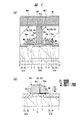
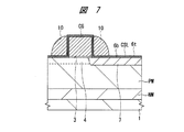
本発明の実施の形態1であるメモリセルの構造の一例を図1および図2によって説明する。図1はメモリセルの要部平面図、図2(a)はチャネルを制御ゲート電極に対して交差する方向(図1のA−A′線)に沿って切断したメモリセルの要部断面図、図2(b)は同図(a)のメモリセルの一部を拡大して示す要部断面図である。ここでは、スプリットゲート構造のサイドウォール方式制御ゲート電極乗り上げ型のメモリセルMC1を例示している。
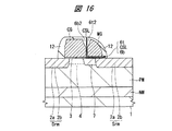
前述の実施の形態1と相違する点は、バーズビーク形状の絶縁膜6b1,6t1を形成する前に、選択ゲート電極CGの上部において選択ゲート電極CGと電荷蓄積層CSLとの間の絶縁膜6bおよび制御ゲート電極MGの上部において制御ゲート電極MGと電荷蓄積層CSLとの間の絶縁膜6tを後退させておき、その後、酸化処理を行うことにより絶縁膜6b2,6t2を形成することにある。
2a 半導体領域
2b 半導体領域
3 ゲート絶縁膜(第1絶縁膜)
4 半導体領域
6b,6b1,6b2 絶縁膜(第2絶縁膜)
6t,6t1,6t2 絶縁膜(第3絶縁膜)
7 半導体領域
10 サイドウォール
11 レジストパターン
12 サイドウォール(第4絶縁膜)
13 絶縁膜
14 シリサイド層
15 絶縁膜
15a 窒化シリコン膜
15b 酸化シリコン膜
ACT 活性領域
CG 選択ゲート電極(第1ゲート電極)
CNT コンタクトホール
CSL 電荷蓄積層
Drm ドレイン領域
M1 第1層配線
MC1 メモリセル
MG 制御ゲート電極(第2ゲート電極)
NW 埋め込みnウェル
PLG プラグ
PW pウェル
Qnc 選択用nMIS(第1電界効果トランジスタ)
Qnm メモリ用nMIS(第2電界効果トランジスタ)
SGI 素子分離部
Srm ソース領域
Claims (5)
- 半導体基板の主面の第1領域に第1電界効果トランジスタを含み、第2領域に前記第1電界効果トランジスタに隣接する第2電界効果トランジスタを含む不揮発性メモリセルを有する半導体装置の製造方法であって、以下の工程を有することを特徴とする半導体装置の製造方法;
(a)前記第1領域上に第1絶縁膜を形成する工程、
(b)前記第1領域上に前記第1絶縁膜を介して第1多結晶シリコンからなる前記第1電界効果トランジスタの第1ゲート電極を形成する工程、
(c)前記(b)工程の後、前記半導体基板上に第2絶縁膜、電荷蓄積層および第3絶縁膜を順次堆積する工程、
(d)前記第3絶縁膜上に第2多結晶シリコンを堆積する工程、
(e)前記第2領域上に前記第2絶縁膜、前記電荷蓄積層および前記第3絶縁膜を介して前記第2多結晶シリコンからなる前記第2電界効果トランジスタの第2ゲート電極を形成する工程、
(f)前記(e)工程の後、前記第2領域上の前記第2絶縁膜、前記電荷蓄積層および前記第3絶縁膜を残して、その他の領域上の前記第2絶縁膜、前記電荷蓄積層および前記第3絶縁膜を除去する工程、
(g)前記第1ゲート電極と前記半導体基板との間の露出する前記第1絶縁膜の側面、ならびに前記第2ゲート電極と前記半導体基板との間の露出する前記第2絶縁膜、前記電荷蓄積層および前記第3絶縁膜の側面を第4絶縁膜で覆う工程、
(h)前記第1ゲート電極の上部と前記電荷蓄積層との間の前記第2絶縁膜および前記第2ゲート電極の上部と前記電荷蓄積層との間の前記第3絶縁膜を酸化処理によりバーズビーク形状とする工程。 - 請求項1記載の半導体装置の製造方法において、前記(h)工程の前にさらに以下の工程を含むことを特徴とする半導体装置の製造方法;
(i)前記第1ゲート電極の上部と前記電荷蓄積層との間の前記第2絶縁膜および前記第2ゲート電極の上部と前記電荷蓄積層との間の前記第3絶縁膜を所定量エッチングする工程。 - 請求項1記載の半導体装置の製造方法において、前記(h)工程の後の前記第1ゲート電極の上部と前記第2ゲート電極の上部との間の距離が、前記第2ゲート電極と前記半導体基板との間の距離よりも長いことを特徴とする半導体装置の製造方法。
- 請求項1記載の半導体装置の製造方法において、前記電荷蓄積層は窒化シリコンを含むことを特徴とする半導体装置の製造方法。
- 半導体基板の主面の第1領域に第1電界効果トランジスタを含み、第2領域に前記第1電界効果トランジスタに隣接する第2電界効果トランジスタを含む不揮発性メモリセルを有する半導体装置であって、
前記第1領域上に形成された第1絶縁膜と、前記第1領域上に前記第1絶縁膜を介して形成された前記第1電界効果トランジスタの第1ゲート電極と、前記第2領域上に下層から順次形成された第2絶縁膜、電荷蓄積層および第3絶縁膜と、前記第2領域上に前記第2絶縁膜、前記電荷蓄積層および前記第3絶縁膜を介して形成された前記第2電界効果トランジスタの第2ゲート電極とを有し、
前記第1ゲート電極と前記第2ゲート電極との間に前記第2絶縁膜、前記電荷蓄積層および前記第3絶縁膜が形成されており、前記第1ゲート電極の上部と前記電荷蓄積層との間の前記第2絶縁膜および前記第2ゲート電極の上部と前記電荷蓄積層との間の前記第3絶縁膜がバーズビーク形状であることを特徴とする半導体装置。
Priority Applications (1)
| Application Number | Priority Date | Filing Date | Title |
|---|---|---|---|
| JP2006081844A JP5142476B2 (ja) | 2006-03-24 | 2006-03-24 | 半導体装置の製造方法 |
Applications Claiming Priority (1)
| Application Number | Priority Date | Filing Date | Title |
|---|---|---|---|
| JP2006081844A JP5142476B2 (ja) | 2006-03-24 | 2006-03-24 | 半導体装置の製造方法 |
Publications (2)
| Publication Number | Publication Date |
|---|---|
| JP2007258497A true JP2007258497A (ja) | 2007-10-04 |
| JP5142476B2 JP5142476B2 (ja) | 2013-02-13 |
Family
ID=38632424
Family Applications (1)
| Application Number | Title | Priority Date | Filing Date |
|---|---|---|---|
| JP2006081844A Expired - Lifetime JP5142476B2 (ja) | 2006-03-24 | 2006-03-24 | 半導体装置の製造方法 |
Country Status (1)
| Country | Link |
|---|---|
| JP (1) | JP5142476B2 (ja) |
Cited By (9)
| Publication number | Priority date | Publication date | Assignee | Title |
|---|---|---|---|---|
| KR101010437B1 (ko) | 2008-07-15 | 2011-01-21 | 주식회사 동부하이텍 | 플래시 메모리 소자 및 그 제조 방법 |
| JP2011103401A (ja) * | 2009-11-11 | 2011-05-26 | Renesas Electronics Corp | 半導体装置およびその製造方法 |
| JP2011114048A (ja) * | 2009-11-25 | 2011-06-09 | Renesas Electronics Corp | 半導体装置およびその製造方法 |
| JP2012248652A (ja) * | 2011-05-27 | 2012-12-13 | Renesas Electronics Corp | 半導体装置およびその製造方法 |
| JP2015095633A (ja) * | 2013-11-14 | 2015-05-18 | ルネサスエレクトロニクス株式会社 | 半導体装置およびその製造方法 |
| CN104851886A (zh) * | 2014-02-18 | 2015-08-19 | 台湾积体电路制造股份有限公司 | 分栅式存储器件及其制造方法 |
| CN104952875A (zh) * | 2014-03-27 | 2015-09-30 | 联华电子股份有限公司 | 存储单元以及其制作方法 |
| KR20160018417A (ko) | 2014-08-08 | 2016-02-17 | 르네사스 일렉트로닉스 가부시키가이샤 | 반도체 장치의 제조 방법 |
| US9450057B2 (en) | 2014-02-18 | 2016-09-20 | Taiwan Semiconductor Manufacturing Co., Ltd. | Split gate cells for embedded flash memory |
Citations (3)
| Publication number | Priority date | Publication date | Assignee | Title |
|---|---|---|---|---|
| JPS6135551A (ja) * | 1984-07-27 | 1986-02-20 | Hitachi Ltd | 半導体集積回路装置の製造方法 |
| JPS6325967A (ja) * | 1986-07-18 | 1988-02-03 | Hitachi Ltd | 半導体集積回路装置 |
| JP2006041227A (ja) * | 2004-07-28 | 2006-02-09 | Renesas Technology Corp | 半導体装置およびその製造方法 |
-
2006
- 2006-03-24 JP JP2006081844A patent/JP5142476B2/ja not_active Expired - Lifetime
Patent Citations (3)
| Publication number | Priority date | Publication date | Assignee | Title |
|---|---|---|---|---|
| JPS6135551A (ja) * | 1984-07-27 | 1986-02-20 | Hitachi Ltd | 半導体集積回路装置の製造方法 |
| JPS6325967A (ja) * | 1986-07-18 | 1988-02-03 | Hitachi Ltd | 半導体集積回路装置 |
| JP2006041227A (ja) * | 2004-07-28 | 2006-02-09 | Renesas Technology Corp | 半導体装置およびその製造方法 |
Cited By (20)
| Publication number | Priority date | Publication date | Assignee | Title |
|---|---|---|---|---|
| KR101010437B1 (ko) | 2008-07-15 | 2011-01-21 | 주식회사 동부하이텍 | 플래시 메모리 소자 및 그 제조 방법 |
| JP2011103401A (ja) * | 2009-11-11 | 2011-05-26 | Renesas Electronics Corp | 半導体装置およびその製造方法 |
| JP2011114048A (ja) * | 2009-11-25 | 2011-06-09 | Renesas Electronics Corp | 半導体装置およびその製造方法 |
| JP2012248652A (ja) * | 2011-05-27 | 2012-12-13 | Renesas Electronics Corp | 半導体装置およびその製造方法 |
| US9293604B2 (en) | 2013-11-14 | 2016-03-22 | Renesas Electronics Corporation | Semiconductor device and method of manufacturing same |
| JP2015095633A (ja) * | 2013-11-14 | 2015-05-18 | ルネサスエレクトロニクス株式会社 | 半導体装置およびその製造方法 |
| US9406813B2 (en) | 2013-11-14 | 2016-08-02 | Renesas Electronics Corporation | Semiconductor device and method of manufacturing same |
| KR101624423B1 (ko) | 2014-02-18 | 2016-05-25 | 타이완 세미콘덕터 매뉴팩쳐링 컴퍼니 리미티드 | 스플릿 게이트 메모리 디바이스 및 이것의 제조 방법 |
| CN104851886A (zh) * | 2014-02-18 | 2015-08-19 | 台湾积体电路制造股份有限公司 | 分栅式存储器件及其制造方法 |
| US9450057B2 (en) | 2014-02-18 | 2016-09-20 | Taiwan Semiconductor Manufacturing Co., Ltd. | Split gate cells for embedded flash memory |
| US9484351B2 (en) | 2014-02-18 | 2016-11-01 | Taiwan Semiconductor Manufacturing Co., Ltd. | Split gate memory device and method of fabricating the same |
| US10147794B2 (en) | 2014-02-18 | 2018-12-04 | Taiwan Semiconductor Manufacturing Co., Ltd. | Split gate memory device and method of fabricating the same |
| US10516026B2 (en) | 2014-02-18 | 2019-12-24 | Taiwan Semiconductor Manufacturing Co., Ltd. | Split gate memory device and method of fabricating the same |
| US11056566B2 (en) | 2014-02-18 | 2021-07-06 | Taiwan Semiconductor Manufacturing Co., Ltd. | Split gate memory device and method of fabricating the same |
| US11658224B2 (en) | 2014-02-18 | 2023-05-23 | Taiwan Semiconductor Manufacturing Company, Ltd. | Split gate memory device and method of fabricating the same |
| US12336229B2 (en) | 2014-02-18 | 2025-06-17 | Taiwan Semiconductor Manufacturing Company, Ltd. | Split gate memory device and method of fabricating the same |
| CN104952875A (zh) * | 2014-03-27 | 2015-09-30 | 联华电子股份有限公司 | 存储单元以及其制作方法 |
| CN104952875B (zh) * | 2014-03-27 | 2019-07-09 | 联华电子股份有限公司 | 存储单元以及其制作方法 |
| KR20160018417A (ko) | 2014-08-08 | 2016-02-17 | 르네사스 일렉트로닉스 가부시키가이샤 | 반도체 장치의 제조 방법 |
| US9349743B2 (en) | 2014-08-08 | 2016-05-24 | Renesas Electronics Corporation | Method of manufacturing semiconductor device |
Also Published As
| Publication number | Publication date |
|---|---|
| JP5142476B2 (ja) | 2013-02-13 |
Similar Documents
| Publication | Publication Date | Title |
|---|---|---|
| US9443991B2 (en) | Semiconductor device and method of manufacturing the same | |
| JP5734744B2 (ja) | 半導体装置およびその製造方法 | |
| US8461642B2 (en) | Semiconductor device having a nonvolatile memory cell with field effect transistors | |
| CN100369239C (zh) | 半导体器件的制造方法和半导体器件 | |
| JP2007281092A (ja) | 半導体装置およびその製造方法 | |
| JP2011114048A (ja) | 半導体装置およびその製造方法 | |
| JP2005244086A (ja) | 半導体装置及びその製造方法 | |
| JP5707224B2 (ja) | 半導体装置およびその製造方法 | |
| US9633859B2 (en) | Semiconductor device and a manufacturing method thereof | |
| US9583502B2 (en) | Method of manufacturing a semiconductor device | |
| JP2017183304A (ja) | 半導体装置およびその製造方法 | |
| US20080280407A1 (en) | Cmos device with dual polycide gates and method of manufacturing the same | |
| US7986001B2 (en) | Semiconductor memory device and method of manufacturing the same | |
| JP5118887B2 (ja) | 半導体装置およびその製造方法 | |
| JP5142476B2 (ja) | 半導体装置の製造方法 | |
| US10483273B2 (en) | Method of manufacturing semiconductor device | |
| JP5123536B2 (ja) | 半導体装置の製造方法 | |
| JP2014187132A (ja) | 半導体装置 | |
| JP2013004791A (ja) | 半導体装置およびその製造方法 | |
| JP2010205791A (ja) | 半導体装置およびその製造方法 | |
| JP6178129B2 (ja) | 半導体装置の製造方法 | |
| JP2008098567A (ja) | 不揮発性半導体記憶装置およびその製造方法 | |
| JP2011210777A (ja) | 半導体装置およびその製造方法 | |
| JP2013021171A (ja) | 半導体装置およびその製造方法 | |
| JP2004214327A (ja) | 半導体装置およびその製造方法 |
Legal Events
| Date | Code | Title | Description |
|---|---|---|---|
| A621 | Written request for application examination |
Free format text: JAPANESE INTERMEDIATE CODE: A621 Effective date: 20090309 |
|
| A711 | Notification of change in applicant |
Free format text: JAPANESE INTERMEDIATE CODE: A712 Effective date: 20100528 |
|
| A977 | Report on retrieval |
Free format text: JAPANESE INTERMEDIATE CODE: A971007 Effective date: 20110210 |
|
| A131 | Notification of reasons for refusal |
Free format text: JAPANESE INTERMEDIATE CODE: A131 Effective date: 20110308 |
|
| A521 | Request for written amendment filed |
Free format text: JAPANESE INTERMEDIATE CODE: A523 Effective date: 20110502 |
|
| A02 | Decision of refusal |
Free format text: JAPANESE INTERMEDIATE CODE: A02 Effective date: 20110719 |
|
| A521 | Request for written amendment filed |
Free format text: JAPANESE INTERMEDIATE CODE: A523 Effective date: 20111017 |
|
| A911 | Transfer to examiner for re-examination before appeal (zenchi) |
Free format text: JAPANESE INTERMEDIATE CODE: A911 Effective date: 20111024 |
|
| A912 | Re-examination (zenchi) completed and case transferred to appeal board |
Free format text: JAPANESE INTERMEDIATE CODE: A912 Effective date: 20111111 |
|
| A521 | Request for written amendment filed |
Free format text: JAPANESE INTERMEDIATE CODE: A523 Effective date: 20121001 |
|
| A01 | Written decision to grant a patent or to grant a registration (utility model) |
Free format text: JAPANESE INTERMEDIATE CODE: A01 |
|
| A61 | First payment of annual fees (during grant procedure) |
Free format text: JAPANESE INTERMEDIATE CODE: A61 Effective date: 20121120 |
|
| FPAY | Renewal fee payment (event date is renewal date of database) |
Free format text: PAYMENT UNTIL: 20151130 Year of fee payment: 3 |
|
| R150 | Certificate of patent or registration of utility model |
Ref document number: 5142476 Country of ref document: JP Free format text: JAPANESE INTERMEDIATE CODE: R150 Free format text: JAPANESE INTERMEDIATE CODE: R150 |
|
| S531 | Written request for registration of change of domicile |
Free format text: JAPANESE INTERMEDIATE CODE: R313531 |
|
| R350 | Written notification of registration of transfer |
Free format text: JAPANESE INTERMEDIATE CODE: R350 |