JP2007261004A - 回折光学素子の射出成形金型及び回折光学素子の製造方法 - Google Patents
回折光学素子の射出成形金型及び回折光学素子の製造方法 Download PDFInfo
- Publication number
- JP2007261004A JP2007261004A JP2006087273A JP2006087273A JP2007261004A JP 2007261004 A JP2007261004 A JP 2007261004A JP 2006087273 A JP2006087273 A JP 2006087273A JP 2006087273 A JP2006087273 A JP 2006087273A JP 2007261004 A JP2007261004 A JP 2007261004A
- Authority
- JP
- Japan
- Prior art keywords
- mold
- optical element
- molding
- injection
- diffractive optical
- Prior art date
- Legal status (The legal status is an assumption and is not a legal conclusion. Google has not performed a legal analysis and makes no representation as to the accuracy of the status listed.)
- Pending
Links
- 230000003287 optical effect Effects 0.000 title claims abstract description 75
- 238000001746 injection moulding Methods 0.000 title abstract description 7
- 238000004519 manufacturing process Methods 0.000 title abstract description 5
- 239000011347 resin Substances 0.000 claims abstract description 52
- 229920005989 resin Polymers 0.000 claims abstract description 52
- 239000000463 material Substances 0.000 claims abstract description 36
- 238000002347 injection Methods 0.000 claims description 13
- 239000007924 injection Substances 0.000 claims description 13
- 238000000465 moulding Methods 0.000 abstract description 5
- 238000012856 packing Methods 0.000 abstract 1
- 239000000243 solution Substances 0.000 abstract 1
- 239000013307 optical fiber Substances 0.000 description 14
- 238000004891 communication Methods 0.000 description 12
- 230000002457 bidirectional effect Effects 0.000 description 9
- 230000005540 biological transmission Effects 0.000 description 4
- 230000008602 contraction Effects 0.000 description 4
- 238000001816 cooling Methods 0.000 description 3
- 238000000034 method Methods 0.000 description 3
- 238000010586 diagram Methods 0.000 description 2
- 239000000835 fiber Substances 0.000 description 1
- 238000007493 shaping process Methods 0.000 description 1
Images


Landscapes
- Diffracting Gratings Or Hologram Optical Elements (AREA)
- Moulds For Moulding Plastics Or The Like (AREA)
Abstract
【解決手段】回折格子パターンが形成された第1の金型と、当該第1の金型に対向する第2の金型とにより形成された空間内に樹脂材を充填して回折光学素子を成形する回折光学素子の射出成形金型において、前記回折格子パターンは、直線状であり、第1の金型の回折格子パターンが形成される部位から第1の金型の樹脂流入部の中心に向かう方向に対して平行に設けられている。
【選択図】図5
Description
図1は、本実施形態に係る双方向光通信モジュールを半割にして、内部を示す斜視図である。図2は、本実施形態に係る双方向光通信モジュールの概略の断面図である。
[第1の実施形態]
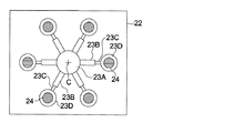
図4は、本実施形態に係る成形金型の断面図である。図4(a)に示すように、上型21と下型22とを合わせた状態で、型内には、上型21の上面から図の下方に向かって拡がるように延在する中央通路23Aと、中央通路23Aの下端近傍から放射状に伸びる分配通路23Bと、分配通路23Bの延長線上に配置されたキャビティ23Dと、キャビティ23Dと分配通路23Bとの間を結ぶ、分配通路23Bより断面積の小さいゲート通路23Cとが形成されている。
第1の実施形態とは、金型における中央通路23A、分配通路23B、ゲート通路23C及びキャビティ23Dの配置が異なっている以外は、基本的に第1の実施形態と同様である。第1の実施形態と同一の部分には同一の符号を付し、第1の実施形態と異なる部分についてのみ説明する。
第1の実施形態とは、金型における中央通路23A、分配通路23B、ゲート通路23C及びキャビティ23Dの配置が異なっている以外は、基本的に第1の実施形態と同様である。第1の実施形態と同一の部分には同一の符号を付し、第1の実施形態と異なる部分についてのみ説明する。
15 エシュロン格子
21 上型
22 下型
23A 中央通路
24 エシュロン格子パターン
34 光学素子素材
Claims (4)
- 回折格子パターンが形成された第1の金型と、当該第1の金型に対向する第2の金型とにより形成される空間内に樹脂材を充填して回折光学素子を成形する回折光学素子の射出成形金型において、
前記回折格子パターンは、直線状であり、前記第1の金型の前記回折格子パターンが形成される部位から前記第1の金型の樹脂流入部の中心に向かう方向に対して平行に設けられていることを特徴とする回折光学素子の射出成形金型。 - 前記第1の金型の前記回折格子パターンが形成される部位は、回転可能に構成されていることを特徴とする請求項1に記載の回折光学素子の射出成形金型。
- 回折格子パターンが形成された第1の金型と、当該第1の金型に対向する第2の金型とにより形成された空間内に樹脂材を充填して回折光学素子を成形する回折光学素子の射出成形金型において、
前記回折格子パターンは、直線状であり、前記第1の金型と前記第2の金型との型開き時に前記回折格子パターンと接触する樹脂材が収縮する方向に対して平行に設けられていることを特徴とする回折光学素子の射出成形金型。 - 請求項1〜3の何れか1項に記載の回折光学素子の射出成形金型を用いて回折光学素子を製造することを特徴とする回折光学素子の製造方法。
Priority Applications (1)
| Application Number | Priority Date | Filing Date | Title |
|---|---|---|---|
| JP2006087273A JP2007261004A (ja) | 2006-03-28 | 2006-03-28 | 回折光学素子の射出成形金型及び回折光学素子の製造方法 |
Applications Claiming Priority (1)
| Application Number | Priority Date | Filing Date | Title |
|---|---|---|---|
| JP2006087273A JP2007261004A (ja) | 2006-03-28 | 2006-03-28 | 回折光学素子の射出成形金型及び回折光学素子の製造方法 |
Publications (1)
| Publication Number | Publication Date |
|---|---|
| JP2007261004A true JP2007261004A (ja) | 2007-10-11 |
Family
ID=38634484
Family Applications (1)
| Application Number | Title | Priority Date | Filing Date |
|---|---|---|---|
| JP2006087273A Pending JP2007261004A (ja) | 2006-03-28 | 2006-03-28 | 回折光学素子の射出成形金型及び回折光学素子の製造方法 |
Country Status (1)
| Country | Link |
|---|---|
| JP (1) | JP2007261004A (ja) |
Cited By (1)
| Publication number | Priority date | Publication date | Assignee | Title |
|---|---|---|---|---|
| US10649157B2 (en) | 2018-08-17 | 2020-05-12 | Foxconn Interconnect Technology Limited | Freeform diffractive optical element (DOE) for use in an optical transmitter and method of designing and manufacturing the freeform DOE |
Citations (3)
| Publication number | Priority date | Publication date | Assignee | Title |
|---|---|---|---|---|
| JPH0455282Y2 (ja) * | 1988-06-03 | 1992-12-25 | ||
| JP2002090518A (ja) * | 2000-09-20 | 2002-03-27 | Olympus Optical Co Ltd | 回折光学素子及び回折光学素子の成形用金型 |
| JP2005274712A (ja) * | 2004-03-23 | 2005-10-06 | Sanyo Electric Co Ltd | 光学素子およびその作製方法 |
-
2006
- 2006-03-28 JP JP2006087273A patent/JP2007261004A/ja active Pending
Patent Citations (3)
| Publication number | Priority date | Publication date | Assignee | Title |
|---|---|---|---|---|
| JPH0455282Y2 (ja) * | 1988-06-03 | 1992-12-25 | ||
| JP2002090518A (ja) * | 2000-09-20 | 2002-03-27 | Olympus Optical Co Ltd | 回折光学素子及び回折光学素子の成形用金型 |
| JP2005274712A (ja) * | 2004-03-23 | 2005-10-06 | Sanyo Electric Co Ltd | 光学素子およびその作製方法 |
Cited By (1)
| Publication number | Priority date | Publication date | Assignee | Title |
|---|---|---|---|---|
| US10649157B2 (en) | 2018-08-17 | 2020-05-12 | Foxconn Interconnect Technology Limited | Freeform diffractive optical element (DOE) for use in an optical transmitter and method of designing and manufacturing the freeform DOE |
Similar Documents
| Publication | Publication Date | Title |
|---|---|---|
| JP5127546B2 (ja) | 光コネクタ | |
| KR100844068B1 (ko) | 광전송 모듈 및 그 제조방법 | |
| US9020352B2 (en) | Optical communication module | |
| KR101001277B1 (ko) | 파장 분할 다중화 광 모듈 | |
| JP4238600B2 (ja) | デマルチプレクサ及び波長多重光伝送モジュール | |
| KR101721851B1 (ko) | 양방향 광모듈 | |
| JP6518113B2 (ja) | 光電気変換コネクタ及びその製造方法 | |
| WO2012169586A1 (ja) | 光レセプタクルおよびこれを備えた光モジュール | |
| JP4221965B2 (ja) | 回折格子、波長合分波器及びこれらを用いた波長多重信号光伝送モジュール | |
| CN113835165A (zh) | 一种光发射组件、芯片、光模块及光通信设备 | |
| CN105849611B (zh) | 光插座及光模块 | |
| JP2007261004A (ja) | 回折光学素子の射出成形金型及び回折光学素子の製造方法 | |
| WO2015125729A1 (ja) | 光レセプタクルおよび光モジュール | |
| CN209913929U (zh) | 一种感光组件、拼版以及摄像模组 | |
| JP4894579B2 (ja) | レンズ筐体及び光モジュール | |
| US7391955B2 (en) | Optical element and optical element holder | |
| KR101896698B1 (ko) | 다채널 광수신모듈의 패키징 방법 및 그 패키지 | |
| JP5428913B2 (ja) | 光接続器及びその製造方法 | |
| JP4903112B2 (ja) | 光路変換部材およびその組立方法 | |
| JP2009047738A (ja) | 光モジュール及びその製造方法 | |
| JP5282988B2 (ja) | 光コネクタ | |
| JPWO2006134794A1 (ja) | 光双方向モジュール | |
| JP4806290B2 (ja) | レンズアレイ成形用金型およびそれを用いたレンズアレイの製造方法 | |
| US20250062591A1 (en) | Encapsulation of side-emitting laser packages by means of vacuum injection molding | |
| US7481587B2 (en) | Optical element, mold for the optical element, method for manufacturing the optical element and bidirectional optical communication module |
Legal Events
| Date | Code | Title | Description |
|---|---|---|---|
| A621 | Written request for application examination |
Free format text: JAPANESE INTERMEDIATE CODE: A621 Effective date: 20090310 |
|
| RD02 | Notification of acceptance of power of attorney |
Free format text: JAPANESE INTERMEDIATE CODE: A7422 Effective date: 20110210 |
|
| A977 | Report on retrieval |
Free format text: JAPANESE INTERMEDIATE CODE: A971007 Effective date: 20110916 |
|
| A131 | Notification of reasons for refusal |
Free format text: JAPANESE INTERMEDIATE CODE: A131 Effective date: 20110927 |
|
| A02 | Decision of refusal |
Free format text: JAPANESE INTERMEDIATE CODE: A02 Effective date: 20120214 |