JP2007281097A - 露光装置及びデバイス製造方法 - Google Patents
露光装置及びデバイス製造方法 Download PDFInfo
- Publication number
- JP2007281097A JP2007281097A JP2006103627A JP2006103627A JP2007281097A JP 2007281097 A JP2007281097 A JP 2007281097A JP 2006103627 A JP2006103627 A JP 2006103627A JP 2006103627 A JP2006103627 A JP 2006103627A JP 2007281097 A JP2007281097 A JP 2007281097A
- Authority
- JP
- Japan
- Prior art keywords
- substrate
- measurement
- shot
- exposure apparatus
- exposure
- Prior art date
- Legal status (The legal status is an assumption and is not a legal conclusion. Google has not performed a legal analysis and makes no representation as to the accuracy of the status listed.)
- Granted
Links
Images






Classifications
-
- H—ELECTRICITY
- H10—SEMICONDUCTOR DEVICES; ELECTRIC SOLID-STATE DEVICES NOT OTHERWISE PROVIDED FOR
- H10P—GENERIC PROCESSES OR APPARATUS FOR THE MANUFACTURE OR TREATMENT OF DEVICES COVERED BY CLASS H10
- H10P76/00—Manufacture or treatment of masks on semiconductor bodies, e.g. by lithography or photolithography
- H10P76/20—Manufacture or treatment of masks on semiconductor bodies, e.g. by lithography or photolithography of masks comprising organic materials
- H10P76/204—Manufacture or treatment of masks on semiconductor bodies, e.g. by lithography or photolithography of masks comprising organic materials of organic photoresist masks
- H10P76/2041—Photolithographic processes
-
- G—PHYSICS
- G03—PHOTOGRAPHY; CINEMATOGRAPHY; ANALOGOUS TECHNIQUES USING WAVES OTHER THAN OPTICAL WAVES; ELECTROGRAPHY; HOLOGRAPHY
- G03F—PHOTOMECHANICAL PRODUCTION OF TEXTURED OR PATTERNED SURFACES, e.g. FOR PRINTING, FOR PROCESSING OF SEMICONDUCTOR DEVICES; MATERIALS THEREFOR; ORIGINALS THEREFOR; APPARATUS SPECIALLY ADAPTED THEREFOR
- G03F7/00—Photomechanical, e.g. photolithographic, production of textured or patterned surfaces, e.g. printing surfaces; Materials therefor, e.g. comprising photoresists; Apparatus specially adapted therefor
- G03F7/70—Microphotolithographic exposure; Apparatus therefor
- G03F7/70691—Handling of masks or workpieces
- G03F7/70716—Stages
- G03F7/70725—Stages control
-
- G—PHYSICS
- G03—PHOTOGRAPHY; CINEMATOGRAPHY; ANALOGOUS TECHNIQUES USING WAVES OTHER THAN OPTICAL WAVES; ELECTROGRAPHY; HOLOGRAPHY
- G03F—PHOTOMECHANICAL PRODUCTION OF TEXTURED OR PATTERNED SURFACES, e.g. FOR PRINTING, FOR PROCESSING OF SEMICONDUCTOR DEVICES; MATERIALS THEREFOR; ORIGINALS THEREFOR; APPARATUS SPECIALLY ADAPTED THEREFOR
- G03F9/00—Registration or positioning of originals, masks, frames, photographic sheets or textured or patterned surfaces, e.g. automatically
- G03F9/70—Registration or positioning of originals, masks, frames, photographic sheets or textured or patterned surfaces, e.g. automatically for microlithography
- G03F9/7003—Alignment type or strategy, e.g. leveling, global alignment
-
- G—PHYSICS
- G03—PHOTOGRAPHY; CINEMATOGRAPHY; ANALOGOUS TECHNIQUES USING WAVES OTHER THAN OPTICAL WAVES; ELECTROGRAPHY; HOLOGRAPHY
- G03F—PHOTOMECHANICAL PRODUCTION OF TEXTURED OR PATTERNED SURFACES, e.g. FOR PRINTING, FOR PROCESSING OF SEMICONDUCTOR DEVICES; MATERIALS THEREFOR; ORIGINALS THEREFOR; APPARATUS SPECIALLY ADAPTED THEREFOR
- G03F9/00—Registration or positioning of originals, masks, frames, photographic sheets or textured or patterned surfaces, e.g. automatically
- G03F9/70—Registration or positioning of originals, masks, frames, photographic sheets or textured or patterned surfaces, e.g. automatically for microlithography
- G03F9/7003—Alignment type or strategy, e.g. leveling, global alignment
- G03F9/7023—Aligning or positioning in direction perpendicular to substrate surface
- G03F9/7034—Leveling
-
- G—PHYSICS
- G03—PHOTOGRAPHY; CINEMATOGRAPHY; ANALOGOUS TECHNIQUES USING WAVES OTHER THAN OPTICAL WAVES; ELECTROGRAPHY; HOLOGRAPHY
- G03F—PHOTOMECHANICAL PRODUCTION OF TEXTURED OR PATTERNED SURFACES, e.g. FOR PRINTING, FOR PROCESSING OF SEMICONDUCTOR DEVICES; MATERIALS THEREFOR; ORIGINALS THEREFOR; APPARATUS SPECIALLY ADAPTED THEREFOR
- G03F9/00—Registration or positioning of originals, masks, frames, photographic sheets or textured or patterned surfaces, e.g. automatically
- G03F9/70—Registration or positioning of originals, masks, frames, photographic sheets or textured or patterned surfaces, e.g. automatically for microlithography
- G03F9/7003—Alignment type or strategy, e.g. leveling, global alignment
- G03F9/7046—Strategy, e.g. mark, sensor or wavelength selection
-
- G—PHYSICS
- G03—PHOTOGRAPHY; CINEMATOGRAPHY; ANALOGOUS TECHNIQUES USING WAVES OTHER THAN OPTICAL WAVES; ELECTROGRAPHY; HOLOGRAPHY
- G03F—PHOTOMECHANICAL PRODUCTION OF TEXTURED OR PATTERNED SURFACES, e.g. FOR PRINTING, FOR PROCESSING OF SEMICONDUCTOR DEVICES; MATERIALS THEREFOR; ORIGINALS THEREFOR; APPARATUS SPECIALLY ADAPTED THEREFOR
- G03F9/00—Registration or positioning of originals, masks, frames, photographic sheets or textured or patterned surfaces, e.g. automatically
- G03F9/70—Registration or positioning of originals, masks, frames, photographic sheets or textured or patterned surfaces, e.g. automatically for microlithography
- G03F9/7073—Alignment marks and their environment
- G03F9/7084—Position of mark on substrate, i.e. position in (x, y, z) of mark, e.g. buried or resist covered mark, mark on rearside, at the substrate edge, in the circuit area, latent image mark, marks in plural levels
Landscapes
- Physics & Mathematics (AREA)
- General Physics & Mathematics (AREA)
- Exposure And Positioning Against Photoresist Photosensitive Materials (AREA)
- Exposure Of Semiconductors, Excluding Electron Or Ion Beam Exposure (AREA)
Abstract
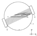
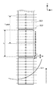
【解決手段】露光装置は、感光剤が塗布された基板の複数のショット領域を投影光学系を介して順に露光する。露光装置は、基板が走査駆動された状態で、連続する複数のショット領域内に定義された計測点の面位置を計測する計測器と、計測器による計測結果に基づいて、基板の被露光領域が投影光学系の像面に一致するように基板の面位置を制御する制御部とを備える。複数のショット領域401、402において、計測点を共通の配置とする。
【選択図】図4
Description
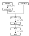
前記現像された基板を処理する処理工程とを含む。
K=INT((L−M)/P)
である。なお、INT( )は、小数点以下を切り捨てる演算記号とする。
D=Ypitch−K×P
である。
ΔT=T2−T1=(D−P)/S
となる。つまり、ショット領域内の最後の計測点を計測してから次のショット領域の最初の計測点を計測するまでに、ショット内計測時間隔T1にΔTを加えた時間を待つことになる。
2 原版
3 原版ステージ機構
4 基板
5 基板チャック
6 露光ステージ機構
7 定盤
8 照明光学系
9 基準面
10 光源
11 コリメータレンズ
12 スリット部材
13、16 光学系
14、15 ミラー
17 ストッパー絞り
18 補正光学系群
19 光電センサ
20 XYバーミラー
21 干渉計
22 計測ステージ機構
23 合焦用マーク
24 ハーフミラー
25 集光レンズ
26 検出器
27a、27b ステージバーミラー
28a、28b 干渉計
50 第1面位置検出ユニット
100 第2面位置検出ユニット
110 メイン制御部
120a、120b ドライバ
130 メモリ
Claims (9)
- 感光剤が塗布された基板の複数のショット領域を投影光学系を介して順に露光する露光装置であって、
基板が走査駆動された状態で、連続する複数のショット領域内に定義された計測点の面位置を計測する計測器と、
前記計測器による計測結果に基づいて、基板の被露光領域が前記投影光学系の像面に一致するように基板の面位置を制御する制御部とを備え、
複数のショット領域のそれぞれについて少なくとも1つの計測点が定義され、複数のショット領域において計測点の配置が共通していることを特徴とする露光装置。 - ショット領域の端から当該ショット領域内の計測点までの距離が複数のショット領域において共通していることを特徴とする請求項1に記載の露光装置。
- ショット領域内の隣接する計測点の間隔が共通の第1距離になり、ショット領域内の最後の計測点と次のショット内の最初の計測点との間隔が第2距離となるように、複数の計測点が定義されることを特徴とする請求項1又は2に記載の露光装置。
- 前記計測器は、基板が等速度で走査駆動された状態で、走査駆動方向に沿って連続して配列された少なくとも2つのショット領域内の計測点の高さを計測することを特徴とする請求項1乃至3のいずれか1項に記載の露光装置。
- 前記計測器は、基板が等速度で走査駆動された状態で、走査駆動方向に沿って連続して配列された第1および第2ショット領域内の計測点の高さを計測することを特徴とする請求項1乃至3のいずれか1項に記載の露光装置。
- 前記計測器は、
前記第1ショット領域内の隣接する計測点及び前記第2ショット領域内の隣接する計測点を共通の第1時間間隔で計測し、
前記第1ショット内の最後の計測点を計測する時刻と前記第2ショット内の最初の計測点を計測する時刻との間に第2時間間隔を確保する、
ことを特徴とする請求項5に記載の露光装置。 - 基板を保持し、かつ基板を露光するための露光ステーションと前記計測器による計測を実施するための計測ステーションとの間を移動する基板ステージを備えることを特徴とする請求項1乃至6のいずれか1項に記載の露光装置。
- 前記基板ステージを複数備え、前記露光ステーションでの基板の露光処理と、前記計測ステーションでの基板の計測処理とが並列に実施されることを特徴とする請求項7に記載の露光装置。
- デバイス製造方法であって、
請求項1乃至8のいずれか1項に記載の露光装置を用いて基板を露光する露光工程と、
前記露光された基板を現像する現像工程と、
前記現像された基板を処理する処理工程と、
を含むことを特徴とするデバイス製造方法。
Priority Applications (6)
| Application Number | Priority Date | Filing Date | Title |
|---|---|---|---|
| JP2006103627A JP4315455B2 (ja) | 2006-04-04 | 2006-04-04 | 露光装置及びデバイス製造方法 |
| US11/692,471 US7423726B2 (en) | 2006-04-04 | 2007-03-28 | Exposure apparatus and device manufacturing method |
| EP07105473A EP1843209A3 (en) | 2006-04-04 | 2007-04-02 | Exposure apparatus and device manufacturing method |
| TW096111915A TWI397778B (zh) | 2006-04-04 | 2007-04-03 | 曝光設備和製造裝置的方法 |
| KR1020070032613A KR100875008B1 (ko) | 2006-04-04 | 2007-04-03 | 노광장치 및 디바이스 제조방법 |
| US12/198,179 US8107052B2 (en) | 2006-04-04 | 2008-08-26 | Exposure apparatus and device manufacturing method |
Applications Claiming Priority (1)
| Application Number | Priority Date | Filing Date | Title |
|---|---|---|---|
| JP2006103627A JP4315455B2 (ja) | 2006-04-04 | 2006-04-04 | 露光装置及びデバイス製造方法 |
Related Child Applications (1)
| Application Number | Title | Priority Date | Filing Date |
|---|---|---|---|
| JP2009051286A Division JP5137879B2 (ja) | 2009-03-04 | 2009-03-04 | 露光装置及びデバイス製造方法 |
Publications (2)
| Publication Number | Publication Date |
|---|---|
| JP2007281097A true JP2007281097A (ja) | 2007-10-25 |
| JP4315455B2 JP4315455B2 (ja) | 2009-08-19 |
Family
ID=38239897
Family Applications (1)
| Application Number | Title | Priority Date | Filing Date |
|---|---|---|---|
| JP2006103627A Expired - Fee Related JP4315455B2 (ja) | 2006-04-04 | 2006-04-04 | 露光装置及びデバイス製造方法 |
Country Status (5)
| Country | Link |
|---|---|
| US (2) | US7423726B2 (ja) |
| EP (1) | EP1843209A3 (ja) |
| JP (1) | JP4315455B2 (ja) |
| KR (1) | KR100875008B1 (ja) |
| TW (1) | TWI397778B (ja) |
Cited By (3)
| Publication number | Priority date | Publication date | Assignee | Title |
|---|---|---|---|---|
| JP2011035333A (ja) * | 2009-08-05 | 2011-02-17 | Renesas Electronics Corp | 走査型露光装置、走査型露光方法、半導体装置の製造方法およびプログラム |
| TWI509369B (zh) * | 2012-07-31 | 2015-11-21 | 佳能股份有限公司 | 曝光方法、曝光設備、和製造裝置的方法 |
| JP2021128949A (ja) * | 2020-02-10 | 2021-09-02 | 株式会社デンソー | ワイドバンドギャップ半導体装置の製造方法 |
Families Citing this family (23)
| Publication number | Priority date | Publication date | Assignee | Title |
|---|---|---|---|---|
| JP4418699B2 (ja) * | 2004-03-24 | 2010-02-17 | キヤノン株式会社 | 露光装置 |
| JP4315455B2 (ja) * | 2006-04-04 | 2009-08-19 | キヤノン株式会社 | 露光装置及びデバイス製造方法 |
| JP2009117419A (ja) * | 2007-11-01 | 2009-05-28 | Canon Inc | 露光装置及びデバイス製造方法 |
| NL1036557A1 (nl) | 2008-03-11 | 2009-09-14 | Asml Netherlands Bv | Method and lithographic apparatus for measuring and acquiring height data relating to a substrate surface. |
| USD597608S1 (en) | 2008-05-19 | 2009-08-04 | Pharmedium Services, Llc | Drug administration safety label |
| JP2009295932A (ja) * | 2008-06-09 | 2009-12-17 | Canon Inc | 露光装置及びデバイス製造方法 |
| JP5335380B2 (ja) * | 2008-11-14 | 2013-11-06 | キヤノン株式会社 | 露光装置およびデバイス製造方法 |
| EP2228685B1 (en) * | 2009-03-13 | 2018-06-27 | ASML Netherlands B.V. | Level sensor arrangement for lithographic apparatus and device manufacturing method |
| US8675210B2 (en) | 2009-03-13 | 2014-03-18 | Asml Netherlands B.V. | Level sensor, lithographic apparatus, and substrate surface positioning method |
| US8488107B2 (en) | 2009-03-13 | 2013-07-16 | Asml Netherlands B.V. | Lithographic apparatus and device manufacturing method involving a level sensor having multiple projection units and detection units |
| US20110174086A1 (en) * | 2010-01-19 | 2011-07-21 | Divyasimha Harish | Capacitive sensor based structure and method with tilt compensation capability |
| NL2006130A (en) * | 2010-03-12 | 2011-09-13 | Asml Netherlands Bv | Lithographic apparatus and device manufacturing method. |
| CN102866587B (zh) * | 2011-07-08 | 2014-12-17 | 上海微电子装备有限公司 | 工件台 |
| US11885738B1 (en) | 2013-01-22 | 2024-01-30 | J.A. Woollam Co., Inc. | Reflectometer, spectrophotometer, ellipsometer or polarimeter system including sample imaging system that simultaneously meet the scheimpflug condition and overcomes keystone error |
| CN104111596A (zh) * | 2013-04-16 | 2014-10-22 | 上海微电子装备有限公司 | 用于光刻设备的全局调平的装置和方法 |
| JP6299111B2 (ja) * | 2013-08-28 | 2018-03-28 | オムロン株式会社 | レーザ加工装置 |
| US10812695B2 (en) * | 2015-09-14 | 2020-10-20 | Nikon Corporation | Three-dimensional positioning system using surface pattern recognition and interpolation |
| US9726987B2 (en) | 2014-04-17 | 2017-08-08 | Nikon Corporation | Positioning system using surface pattern recognition and interpolation |
| US11061338B2 (en) | 2014-04-17 | 2021-07-13 | Nikon Corporation | High-resolution position encoder with image sensor and encoded target pattern |
| JP6748461B2 (ja) * | 2016-03-22 | 2020-09-02 | キヤノン株式会社 | インプリント装置、インプリント装置の動作方法および物品製造方法 |
| CN114184621B (zh) * | 2020-09-14 | 2024-12-17 | 临颍县爬杆机器人有限公司 | 曲面零件外观缺陷检测方法及实施该方法的装置 |
| US11487210B1 (en) * | 2021-08-12 | 2022-11-01 | Taiwan Semiconductor Manufacturing Company Ltd. | Method and system of surface topography measurement for lithography |
| JP2023042984A (ja) * | 2021-09-15 | 2023-03-28 | キヤノン株式会社 | 露光装置、及び物品の製造方法 |
Family Cites Families (13)
| Publication number | Priority date | Publication date | Assignee | Title |
|---|---|---|---|---|
| JP3269343B2 (ja) | 1995-07-26 | 2002-03-25 | キヤノン株式会社 | ベストフォーカス決定方法及びそれを用いた露光条件決定方法 |
| US6559465B1 (en) | 1996-08-02 | 2003-05-06 | Canon Kabushiki Kaisha | Surface position detecting method having a detection timing determination |
| JP3335126B2 (ja) | 1998-07-06 | 2002-10-15 | キヤノン株式会社 | 面位置検出装置及びそれを用いた走査型投影露光装置 |
| JP3913079B2 (ja) | 2002-02-28 | 2007-05-09 | キヤノン株式会社 | 面位置検出装置及び方法並びに露光装置と該露光装置を用いたデバイスの製造方法 |
| KR100888472B1 (ko) | 2002-07-06 | 2009-03-12 | 삼성전자주식회사 | 이중키를 이용한 암호화방법 및 이를 위한 무선 랜 시스템 |
| JP2004071851A (ja) | 2002-08-07 | 2004-03-04 | Canon Inc | 半導体露光方法及び露光装置 |
| JP2004266342A (ja) | 2003-02-03 | 2004-09-24 | Sony Corp | 無線アドホック通信システム、端末、その端末における復号方法、暗号化方法及びブロードキャスト暗号鍵配布方法並びにそれらの方法を端末に実行させるためのプログラム |
| JP4652667B2 (ja) | 2003-02-13 | 2011-03-16 | キヤノン株式会社 | 面位置計測方法及び走査型露光装置 |
| JP4315420B2 (ja) | 2003-04-18 | 2009-08-19 | キヤノン株式会社 | 露光装置及び露光方法 |
| JP2005129674A (ja) | 2003-10-23 | 2005-05-19 | Canon Inc | 走査露光装置およびデバイス製造方法 |
| US7061579B2 (en) * | 2003-11-13 | 2006-06-13 | Asml Netherlands B.V. | Lithographic apparatus and device manufacturing method |
| JP4418699B2 (ja) | 2004-03-24 | 2010-02-17 | キヤノン株式会社 | 露光装置 |
| JP4315455B2 (ja) | 2006-04-04 | 2009-08-19 | キヤノン株式会社 | 露光装置及びデバイス製造方法 |
-
2006
- 2006-04-04 JP JP2006103627A patent/JP4315455B2/ja not_active Expired - Fee Related
-
2007
- 2007-03-28 US US11/692,471 patent/US7423726B2/en not_active Expired - Fee Related
- 2007-04-02 EP EP07105473A patent/EP1843209A3/en not_active Withdrawn
- 2007-04-03 KR KR1020070032613A patent/KR100875008B1/ko not_active Expired - Fee Related
- 2007-04-03 TW TW096111915A patent/TWI397778B/zh not_active IP Right Cessation
-
2008
- 2008-08-26 US US12/198,179 patent/US8107052B2/en not_active Expired - Fee Related
Cited By (4)
| Publication number | Priority date | Publication date | Assignee | Title |
|---|---|---|---|---|
| JP2011035333A (ja) * | 2009-08-05 | 2011-02-17 | Renesas Electronics Corp | 走査型露光装置、走査型露光方法、半導体装置の製造方法およびプログラム |
| TWI509369B (zh) * | 2012-07-31 | 2015-11-21 | 佳能股份有限公司 | 曝光方法、曝光設備、和製造裝置的方法 |
| JP2021128949A (ja) * | 2020-02-10 | 2021-09-02 | 株式会社デンソー | ワイドバンドギャップ半導体装置の製造方法 |
| JP7287304B2 (ja) | 2020-02-10 | 2023-06-06 | 株式会社デンソー | ワイドバンドギャップ半導体装置の製造方法 |
Also Published As
| Publication number | Publication date |
|---|---|
| EP1843209A2 (en) | 2007-10-10 |
| TWI397778B (zh) | 2013-06-01 |
| US8107052B2 (en) | 2012-01-31 |
| EP1843209A3 (en) | 2007-12-05 |
| TW200807164A (en) | 2008-02-01 |
| US20080316450A1 (en) | 2008-12-25 |
| US7423726B2 (en) | 2008-09-09 |
| JP4315455B2 (ja) | 2009-08-19 |
| US20070229788A1 (en) | 2007-10-04 |
| KR20070099464A (ko) | 2007-10-09 |
| KR100875008B1 (ko) | 2008-12-19 |
Similar Documents
| Publication | Publication Date | Title |
|---|---|---|
| JP4315455B2 (ja) | 露光装置及びデバイス製造方法 | |
| JP3376179B2 (ja) | 面位置検出方法 | |
| KR101444981B1 (ko) | 노광 장치, 노광 방법 및 디바이스 제조 방법 | |
| US7528966B2 (en) | Position detection apparatus and exposure apparatus | |
| JP3997068B2 (ja) | リトグラフ投影装置の較正方法およびそのような方法を適用できる装置 | |
| JPH07270122A (ja) | 変位検出装置、該変位検出装置を備えた露光装置およびデバイスの製造方法 | |
| KR102294481B1 (ko) | 이동체의 제어 방법, 노광 방법, 디바이스 제조 방법, 이동체 장치, 및 노광 장치 | |
| HK1225513A1 (zh) | 曝光装置及曝光方法、以及器件制造方法 | |
| JP5137879B2 (ja) | 露光装置及びデバイス製造方法 | |
| JP2001257157A (ja) | アライメント装置、アライメント方法、露光装置、及び露光方法 | |
| JP3335126B2 (ja) | 面位置検出装置及びそれを用いた走査型投影露光装置 | |
| US7852458B2 (en) | Exposure apparatus | |
| KR19980024115A (ko) | 투영 노광 방법 및 투영 노광 장치 | |
| JP2010258085A (ja) | 面位置検出方法 | |
| JP3441930B2 (ja) | 走査型露光装置およびデバイス製造方法 | |
| JP3428825B2 (ja) | 面位置検出方法および面位置検出装置 | |
| US20100110400A1 (en) | Scanning exposure apparatus, control method therefor, and device manufacturing method | |
| JPH104055A (ja) | 自動焦点合わせ装置及びそれを用いたデバイスの製造方法 | |
| JP7699458B2 (ja) | 露光装置、露光方法及び物品の製造方法 | |
| JP3420401B2 (ja) | 位置検出装置および方法、半導体露光装置ならびに半導体デバイスの製造方法 | |
| TW202418001A (zh) | 曝光設備及物品製造方法 | |
| JP2005116581A (ja) | 検出方法、露光方法、検出装置、露光装置、並びにデバイス製造方法 | |
| JP2006253469A (ja) | ステージ装置および露光装置 | |
| JPH1140488A (ja) | 位置合わせ方法 | |
| JP2016149405A (ja) | 計測装置、露光装置、デバイス製造方法、及び計測方法 |
Legal Events
| Date | Code | Title | Description |
|---|---|---|---|
| A621 | Written request for application examination |
Free format text: JAPANESE INTERMEDIATE CODE: A621 Effective date: 20071012 |
|
| RD03 | Notification of appointment of power of attorney |
Free format text: JAPANESE INTERMEDIATE CODE: A7423 Effective date: 20071012 |
|
| A977 | Report on retrieval |
Free format text: JAPANESE INTERMEDIATE CODE: A971007 Effective date: 20080411 |
|
| A131 | Notification of reasons for refusal |
Free format text: JAPANESE INTERMEDIATE CODE: A131 Effective date: 20080418 |
|
| A521 | Request for written amendment filed |
Free format text: JAPANESE INTERMEDIATE CODE: A523 Effective date: 20080609 |
|
| A02 | Decision of refusal |
Free format text: JAPANESE INTERMEDIATE CODE: A02 Effective date: 20090105 |
|
| A521 | Request for written amendment filed |
Free format text: JAPANESE INTERMEDIATE CODE: A523 Effective date: 20090304 |
|
| A911 | Transfer to examiner for re-examination before appeal (zenchi) |
Free format text: JAPANESE INTERMEDIATE CODE: A911 Effective date: 20090313 |
|
| TRDD | Decision of grant or rejection written | ||
| A01 | Written decision to grant a patent or to grant a registration (utility model) |
Free format text: JAPANESE INTERMEDIATE CODE: A01 Effective date: 20090515 |
|
| A01 | Written decision to grant a patent or to grant a registration (utility model) |
Free format text: JAPANESE INTERMEDIATE CODE: A01 |
|
| A61 | First payment of annual fees (during grant procedure) |
Free format text: JAPANESE INTERMEDIATE CODE: A61 Effective date: 20090518 |
|
| R150 | Certificate of patent or registration of utility model |
Ref document number: 4315455 Country of ref document: JP Free format text: JAPANESE INTERMEDIATE CODE: R150 Free format text: JAPANESE INTERMEDIATE CODE: R150 |
|
| FPAY | Renewal fee payment (event date is renewal date of database) |
Free format text: PAYMENT UNTIL: 20120529 Year of fee payment: 3 |
|
| FPAY | Renewal fee payment (event date is renewal date of database) |
Free format text: PAYMENT UNTIL: 20120529 Year of fee payment: 3 |
|
| FPAY | Renewal fee payment (event date is renewal date of database) |
Free format text: PAYMENT UNTIL: 20130529 Year of fee payment: 4 |
|
| FPAY | Renewal fee payment (event date is renewal date of database) |
Free format text: PAYMENT UNTIL: 20140529 Year of fee payment: 5 |
|
| LAPS | Cancellation because of no payment of annual fees |