JP2007281155A - 薄膜トランジスタ、及びその製造方法、並びにアクティブマトリクス型表示装置 - Google Patents
薄膜トランジスタ、及びその製造方法、並びにアクティブマトリクス型表示装置 Download PDFInfo
- Publication number
- JP2007281155A JP2007281155A JP2006104886A JP2006104886A JP2007281155A JP 2007281155 A JP2007281155 A JP 2007281155A JP 2006104886 A JP2006104886 A JP 2006104886A JP 2006104886 A JP2006104886 A JP 2006104886A JP 2007281155 A JP2007281155 A JP 2007281155A
- Authority
- JP
- Japan
- Prior art keywords
- insulating film
- conductive barrier
- barrier layer
- opening
- display device
- Prior art date
- Legal status (The legal status is an assumption and is not a legal conclusion. Google has not performed a legal analysis and makes no representation as to the accuracy of the status listed.)
- Granted
Links
Images




Classifications
-
- H—ELECTRICITY
- H10—SEMICONDUCTOR DEVICES; ELECTRIC SOLID-STATE DEVICES NOT OTHERWISE PROVIDED FOR
- H10D—INORGANIC ELECTRIC SEMICONDUCTOR DEVICES
- H10D30/00—Field-effect transistors [FET]
- H10D30/60—Insulated-gate field-effect transistors [IGFET]
- H10D30/67—Thin-film transistors [TFT]
- H10D30/6758—Thin-film transistors [TFT] characterised by the insulating substrates
-
- H—ELECTRICITY
- H10—SEMICONDUCTOR DEVICES; ELECTRIC SOLID-STATE DEVICES NOT OTHERWISE PROVIDED FOR
- H10D—INORGANIC ELECTRIC SEMICONDUCTOR DEVICES
- H10D30/00—Field-effect transistors [FET]
- H10D30/60—Insulated-gate field-effect transistors [IGFET]
- H10D30/67—Thin-film transistors [TFT]
- H10D30/6704—Thin-film transistors [TFT] having supplementary regions or layers in the thin films or in the insulated bulk substrates for controlling properties of the device
-
- H—ELECTRICITY
- H10—SEMICONDUCTOR DEVICES; ELECTRIC SOLID-STATE DEVICES NOT OTHERWISE PROVIDED FOR
- H10D—INORGANIC ELECTRIC SEMICONDUCTOR DEVICES
- H10D86/00—Integrated devices formed in or on insulating or conducting substrates, e.g. formed in silicon-on-insulator [SOI] substrates or on stainless steel or glass substrates
- H10D86/40—Integrated devices formed in or on insulating or conducting substrates, e.g. formed in silicon-on-insulator [SOI] substrates or on stainless steel or glass substrates characterised by multiple TFTs
- H10D86/481—Integrated devices formed in or on insulating or conducting substrates, e.g. formed in silicon-on-insulator [SOI] substrates or on stainless steel or glass substrates characterised by multiple TFTs integrated with passive devices, e.g. auxiliary capacitors
-
- H—ELECTRICITY
- H10—SEMICONDUCTOR DEVICES; ELECTRIC SOLID-STATE DEVICES NOT OTHERWISE PROVIDED FOR
- H10D—INORGANIC ELECTRIC SEMICONDUCTOR DEVICES
- H10D86/00—Integrated devices formed in or on insulating or conducting substrates, e.g. formed in silicon-on-insulator [SOI] substrates or on stainless steel or glass substrates
- H10D86/40—Integrated devices formed in or on insulating or conducting substrates, e.g. formed in silicon-on-insulator [SOI] substrates or on stainless steel or glass substrates characterised by multiple TFTs
- H10D86/60—Integrated devices formed in or on insulating or conducting substrates, e.g. formed in silicon-on-insulator [SOI] substrates or on stainless steel or glass substrates characterised by multiple TFTs wherein the TFTs are in active matrices
Landscapes
- Electroluminescent Light Sources (AREA)
- Devices For Indicating Variable Information By Combining Individual Elements (AREA)
- Thin Film Transistor (AREA)
Abstract
【解決手段】本発明の一態様にかかる薄膜トランジスタは、金属基板1と、金属基板1上に設けられ、金属基板1物質の拡散を防ぐ第1の導電性バリア層2と、第1の導電性バリア層2上に設けられた保護絶縁膜3と、保護絶縁膜3上に設けられ、ソース領域4c、ドレイン領域4a、及びチャネル領域4bを含む半導体層4と、半導体層4の上に設けられたゲート絶縁膜5と、ゲート絶縁膜5を介して半導体層4の上に設けられたゲート電極6とを備え、保護絶縁膜3に設けられた第1の開口部3aを介して第1の導電性バリア層2と半導体層4とが電気的に接続されているものである。
【選択図】図1
Description
Y. R. Luo et al.,"The Electrical Characteristics of Low Temperature Polycrystalline Silicon Thin Film Transistor Fabricated on Stainless Foil", Proceedings of AM-LCD'05, (2005), p.231 N. Young et al.,"LTPS on Passivated Stainless Steel Substrate for AMOLEDs and Other Applications", Proceedings of AM-LCD'05, (2005), p.239
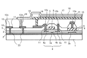
本発明の実施の形態1にかかる薄膜トランジスタを用いたアクティブマトリクス型表示装置について図1を参照して説明する。図1は、本実施の形態にかかるアクティブマトリクス型表示装置の構成を示す断面図である。ここでは、アクティブマトリクス型表示装置の一例として、コプラナ型のTFTを有する有機EL表示装置について説明する。ここでは、有機EL表示装置に用いられる駆動用TFT、及びその周辺の構成について説明する。もちろん、本実施の形態にかかるTFTは、有機EL表示装置の駆動用TFTに対する使用に限られるものではない。
・武山他、「ULSIにおける置換型複合窒化物合金バリヤを用いた一体型極微細Cu配線に関する研究」、NEDO平成14年度研究助成事業(2事業合同)成果報告会予稿集、情報通信技術、B−2、(プロジェクトID:00A22021a)
この文献を考慮して、第1の導電性バリア層2の材料として、高融点金属又は導電性の高融点金属窒化物であるTi、Ta、W、Mo、TiN、TaN、WN、MoN、ZrN、VN、HfN、NbN、TiZrN、ZrVNなどを選択することができる。
・M. Taketama et al., "Solid-Phase Reaction of Diffusion Barriers of Ti and TiN to Copper Layers on SiO2", Jpn. J. Appl. Phys., Vol. 35 (1996), p.4027-4033
・K. Huseyin et al., "TiN and TaN diffusion Brriers in copper interconnect technology: Towards a consistent testing methodology", Jounal of Electronic Materials,Apr 2001
したがって、第1の導電性バリア層2としては、TiN、TaN、ZrN、VNの単層膜や、TiN、TaN、ZrN、VNを上層として積層される複合膜を用いることが好ましい。
本発明の実施の形態2にかかるアクティブマトリクス型表示装置について図2を参照して説明する。図2は、本実施の形態にかかる有機EL表示装置の構成を示す断面図である。本実施の形態において、実施の形態1と異なる点は、保護絶縁膜3に形成された第1の開口部3aが第1の導電性バリア層2により埋め込まれている点である。図2において、図1と同一の構成要素には同一の符号を付し、説明を省略する。
本発明の実施の形態3にかかるアクティブマトリクス型表示装置について図3を参照して説明する。図3は、本実施の形態にかかる有機EL表示装置の構成を示す断面図である。本実施の形態において、実施の形態1、2と異なる点は、保護絶縁膜3に形成された第1の開口部3aの一部又は全部が第1の導電性バリア層2により埋め込まれ、さらに、保護絶縁膜3の上まで延在して設けられている点である。図3において、図1と同一の構成要素には同一の符号を付し、説明を省略する。
本発明の実施の形態4にかかるアクティブマトリクス型表示装置について図4を参照して説明する。図4は、本実施の形態にかかる有機EL表示装置の構成を示す断面図である。本実施の形態において、実施の形態1と異なる点は、キャパシタの構造である。図4において、図1と同一の構成要素には同一の符号を付し、説明を省略する。
本発明の実施の形態5にかかるアクティブマトリクス型表示装置について図5を参照して説明する。図5は、本実施の形態にかかる有機EL表示装置の構成を示す断面図である。本実施の形態において、実施の形態2と異なる点は、キャパシタの構造である。図5において、図1と同一の構成要素には同一の符号を付し、説明を省略する。
本発明の実施の形態6にかかるアクティブマトリクス型表示装置について図6を参照して説明する。図6は、本実施の形態にかかる有機EL表示装置の構成を示す断面図である。本実施の形態において、実施の形態3と異なる点は、キャパシタの構造である。図6において、図1と同一の構成要素には同一の符号を付し、説明を省略する。
本発明の他の実施の形態にかかるアクティブマトリクス型表示装置について図7〜12を参照して説明する。TFT及びキャパシタの構造については、図7〜12はそれぞれ図1〜6に示す構造と略一致しており、異なる点は対向電極18が配線12dを介さず、直接第1の導電性バリア層2と電気的に接続されている点である。従って、図7〜12においては、実施の形態1において説明した配線12dが設けられていない構成となる。
2 第1の導電性バリア層
3 保護絶縁膜
3a 第1の開口部
3b 第2の開口部
4 半導体層
4a ドレイン領域
4b チャネル領域
4c ソース領域
5 ゲート絶縁膜
6 ゲート電極
7 第1のキャパシタ電極
8 キャパシタ絶縁膜
9 第2のキャパシタ電極
10 第1の層間絶縁膜
11 コンタクトホール
12 配線
13 第2の層間絶縁膜
14 コンタクトホール
15 画素電極
16 開口絶縁膜
17 発光層
18 対向電極
19 コンタクトホール
20 第2の導電性バリア層
21 ドレイン電極
22 ソース電極
23 コンタクトホール
Claims (20)
- 金属基板と、
前記金属基板上に設けられ、前記金属基板物質の拡散を防ぐ第1の導電性バリア層と、
前記第1の導電性バリア層上に設けられた保護絶縁膜と、
前記保護絶縁膜上に設けられ、ソース領域、ドレイン領域、及びチャネル領域を含む半導体層と、
前記半導体層の上に設けられたゲート絶縁膜と、
前記ゲート絶縁膜を介して前記半導体層の上に設けられたゲート電極とを備え、
前記保護絶縁膜に設けられた開口部を介して前記第1の導電性バリア層と前記半導体層とが電気的に接続されている薄膜トランジスタ。 - 前記保護絶縁膜に設けられた開口部の少なくとも一部に、前記第1の導電性バリア層が埋め込まれている請求項1に記載の薄膜トランジスタ。
- 前記開口部に埋め込まれた第1の導電性バリア層が、前記保護絶縁膜の上に延在して設けられている請求項2に記載の薄膜トランジスタ。
- 前記第1の導電性バリア層は、高融点金属又は導電性の高融点金属窒化物を含んでいる請求項1乃至3に記載の薄膜トランジスタ。
- 前記第1の導電性バリア層は、Ti、Ta、W、Mo、TiN、TaN、W、MoN、ZrN、VN、HfN、NbN、TiZrN、ZrVNのうちの一つ以上を含む膜である請求項1乃至4のいずれかに記載の薄膜トランジスタ。
- 前記保護絶縁膜は、シリコン酸化膜、シリコン窒化膜及びシリコン窒化酸化膜の内の一つ以上を含む単層膜又は複合膜である請求項1乃至5のいずれか1項記載の薄膜トランジスタ。
- 請求項1乃至6のいずれか1項に記載の薄膜トランジスタと、
前記金属基板上に設けられ、第1のキャパシタ電極と第2のキャパシタ電極とを有するキャパシタとを備えるアクティブマトリクス型表示装置。 - 前記第1のキャパシタ電極が前記半導体層と同一の材料で形成されている請求項7に記載のアクティブマトリクス型表示装置。
- 前記第1のキャパシタ電極と前記保護絶縁膜との間に、第2の導電性バリア層が設けられている請求項7又は8に記載のアクティブマトリクス型表示装置。
- 前記保護絶縁膜には第2の開口部が設けられ、
前記第2の開口部に対応する位置に前記キャパシタが形成され、第1のキャパシタ電極が前記第1の導電性バリア層により形成されている請求項7に記載のアクティブマトリクス型表示装置。 - 前記第1の開口部及び前記第2の開口部それぞれの少なくとも一部には、前記第1の導電性バリア層が埋め込まれている請求項10に記載のアクティブマトリクス型表示装置。
- 前記第1のキャパシタ電極と前記第2のキャパシタ電極との間に配置されたキャパシタ絶縁膜が、前記ゲート絶縁膜と同一の物質で形成されている請求項7乃至11のいずれかに記載のアクティブマトリクス型表示装置。
- 前記ゲート電極と前記第2のキャパシタ電極とは同一の物質で構成されている請求項7乃至12に記載のアクティブマトリクス型表示装置。
- 前記薄膜トランジスタ及び前記キャパシタを覆う第1の層間絶縁膜と、
前記第1の層間絶縁膜に設けられたコンタクトホールを介して前記第1の導電性バリア層と電気的に接続されている配線と、
前記第1の層間絶縁膜及び前記配線を覆う第2の層間絶縁膜と、
前記第2の層間絶縁膜に設けられたコンタクトホールを介して前記ドレイン領域と電気的に接続された画素電極とをさらに備える請求項7乃至13のいずれかに記載のアクティブマトリクス型表示装置。 - 前記第2の層間絶縁膜の表面粗さは100μm2領域のRMS値で50nm以下である請求項14のいずれか1項に記載のアクティブマトリクス型表示装置。
- 前記画素電極の表面粗さは100μm2領域のRMS値で50nm以下である請求項14又は15に記載のアクティブマトリクス型表示装置。
- 前記画素電極に対して発光層を挟んで対向する対向電極を備え、
前記対向電極は前記第2の層間絶縁膜に形成された開口部を介して前記配線若しくは前記第1の導電性バリア層と電気的に接続されている請求項14乃至16のいずれか1項に記載のアクティブマトリクス型表示装置。 - 金属基板上に前記金属基板物質の拡散を防ぐ第1の導電性バリア層を形成し、
前記第1の導電性バリア層の上に、開口部を有する保護絶縁層を形成し、
前記保護絶縁層の開口部を介して前記第1の導電性バリア層と接続される半導体層を形成し、
前記半導体層の上に、ゲート絶縁膜を形成し、
前記ゲート絶縁膜の上にゲート電極を形成する薄膜トランジスタの製造方法。 - 前記保護絶縁膜に設けられた開口部の一部に前記第1の導電性バリア層が埋め込まれている請求項18に記載の薄膜トランジスタの製造方法。
- 前記保護絶縁膜に設けられた開口部の一部、前記半導体層の一部が埋め込まれている請求項18に記載の薄膜トランジスタの製造方法。
Priority Applications (3)
| Application Number | Priority Date | Filing Date | Title |
|---|---|---|---|
| JP2006104886A JP5090658B2 (ja) | 2006-04-06 | 2006-04-06 | 薄膜トランジスタ、及びその製造方法、並びにアクティブマトリクス型表示装置 |
| TW096111768A TW200805670A (en) | 2006-04-06 | 2007-04-03 | Thin film transistor, its manufacturing method, and active matrix display device |
| US11/697,073 US7550771B2 (en) | 2006-04-06 | 2007-04-05 | Thin film transistor, manufacturing method thereof, and active matrix display apparatus |
Applications Claiming Priority (1)
| Application Number | Priority Date | Filing Date | Title |
|---|---|---|---|
| JP2006104886A JP5090658B2 (ja) | 2006-04-06 | 2006-04-06 | 薄膜トランジスタ、及びその製造方法、並びにアクティブマトリクス型表示装置 |
Publications (2)
| Publication Number | Publication Date |
|---|---|
| JP2007281155A true JP2007281155A (ja) | 2007-10-25 |
| JP5090658B2 JP5090658B2 (ja) | 2012-12-05 |
Family
ID=38574292
Family Applications (1)
| Application Number | Title | Priority Date | Filing Date |
|---|---|---|---|
| JP2006104886A Expired - Fee Related JP5090658B2 (ja) | 2006-04-06 | 2006-04-06 | 薄膜トランジスタ、及びその製造方法、並びにアクティブマトリクス型表示装置 |
Country Status (3)
| Country | Link |
|---|---|
| US (1) | US7550771B2 (ja) |
| JP (1) | JP5090658B2 (ja) |
| TW (1) | TW200805670A (ja) |
Cited By (17)
| Publication number | Priority date | Publication date | Assignee | Title |
|---|---|---|---|---|
| JP2009212483A (ja) * | 2008-02-29 | 2009-09-17 | Samsung Mobile Display Co Ltd | フレキシブル基板、その製造方法及びそれを用いた薄膜トランジスタ |
| KR101065412B1 (ko) * | 2009-10-06 | 2011-09-16 | 삼성모바일디스플레이주식회사 | 유기 발광 표시 장치 및 그 제조 방법 |
| KR101074803B1 (ko) * | 2009-11-24 | 2011-10-19 | 삼성모바일디스플레이주식회사 | 유기 발광 표시 장치 및 그 제조 방법 |
| JP2012181445A (ja) * | 2011-03-02 | 2012-09-20 | Seiko Epson Corp | 電気装置 |
| JP2012528488A (ja) * | 2009-05-28 | 2012-11-12 | コヴィオ インコーポレイテッド | 拡散バリアで被覆された基板上の半導体デバイス及びその形成方法 |
| JP2013165132A (ja) * | 2012-02-09 | 2013-08-22 | Semiconductor Energy Lab Co Ltd | 半導体装置 |
| JPWO2013080247A1 (ja) * | 2011-11-29 | 2015-04-27 | パナソニック株式会社 | 薄膜トランジスタおよび薄膜トランジスタの製造方法 |
| KR20160038172A (ko) * | 2014-09-29 | 2016-04-07 | 삼성디스플레이 주식회사 | 박막트랜지스터 기판, 이를 구비한 디스플레이 장치, 박막트랜지스터 기판 제조방법 및 디스플레이 장치 제조방법 |
| KR20180068634A (ko) * | 2016-12-14 | 2018-06-22 | 엘지디스플레이 주식회사 | 유기 발광 표시 장치 |
| JP2019204967A (ja) * | 2019-07-29 | 2019-11-28 | 堺ディスプレイプロダクト株式会社 | 有機el表示装置及びその製造方法 |
| JP2019216236A (ja) * | 2019-05-15 | 2019-12-19 | 堺ディスプレイプロダクト株式会社 | 有機el表示装置及び有機el表示装置の製造方法 |
| JP2020024930A (ja) * | 2018-03-28 | 2020-02-13 | 堺ディスプレイプロダクト株式会社 | 有機el表示装置及びその製造方法 |
| KR20200062510A (ko) * | 2018-11-27 | 2020-06-04 | 엘지디스플레이 주식회사 | 표시 장치 |
| US10997906B2 (en) | 2018-03-28 | 2021-05-04 | Sakai Display Products Corporation | Organic EL display apparatus with reduced surface roughness and electrode having silver and ITO and manufacturing method therefor |
| US11094763B2 (en) | 2018-03-28 | 2021-08-17 | Sakai Display Products Corporation | Organic EL device with alternately lined source drain electrodes |
| US20210332476A1 (en) * | 2020-04-24 | 2021-10-28 | Asm Ip Holding B.V. | Method of forming vanadium nitride–containing layer and structure comprising the same |
| KR20220115708A (ko) * | 2021-02-09 | 2022-08-18 | 삼성디스플레이 주식회사 | 유기발광 디스플레이 장치 |
Families Citing this family (15)
| Publication number | Priority date | Publication date | Assignee | Title |
|---|---|---|---|---|
| US7781306B2 (en) * | 2007-06-20 | 2010-08-24 | Semiconductor Energy Laboratory Co., Ltd. | Semiconductor substrate and method for manufacturing the same |
| US8692251B2 (en) * | 2007-11-02 | 2014-04-08 | Sharp Kabushiki Kaisha | Circuit board and display device |
| US9183973B2 (en) | 2009-05-28 | 2015-11-10 | Thin Film Electronics Asa | Diffusion barrier coated substrates and methods of making the same |
| KR101193197B1 (ko) * | 2010-07-07 | 2012-10-19 | 삼성디스플레이 주식회사 | 유기 발광 표시 장치 및 이의 제조 방법 |
| TWI451179B (zh) * | 2011-11-17 | 2014-09-01 | 友達光電股份有限公司 | 畫素結構及其製造方法 |
| CN105336871A (zh) * | 2014-08-12 | 2016-02-17 | 群创光电股份有限公司 | 显示面板 |
| TWI575732B (zh) * | 2016-05-25 | 2017-03-21 | 友達光電股份有限公司 | 畫素結構及其顯示面板 |
| KR20180004488A (ko) * | 2016-07-04 | 2018-01-12 | 삼성디스플레이 주식회사 | 유기 발광 표시 장치 및 그 제조 방법 |
| US11114517B2 (en) | 2018-03-28 | 2021-09-07 | Sakai Display Products Corporation | Organic EL display apparatus and method of manufacturing organic EL display apparatus |
| US11011593B2 (en) * | 2018-03-28 | 2021-05-18 | Sakai Display Products Corporation | Organic EL display device and manufacturing method for organic EL display device |
| WO2020086532A1 (en) | 2018-10-22 | 2020-04-30 | Thin Film Electronics Asa | Barrier stacks for printed and/or thin film electronics methods of manufacturing the same, and method of controlling a threshold voltage of a thin film transistor |
| JP2020173309A (ja) * | 2019-04-09 | 2020-10-22 | シャープ株式会社 | 液晶パネル |
| KR102899769B1 (ko) * | 2019-12-31 | 2025-12-12 | 엘지디스플레이 주식회사 | 표시 패널 및 이를 이용한 표시 장치 |
| CN111446264B (zh) * | 2020-04-15 | 2023-03-24 | Tcl华星光电技术有限公司 | 阵列基板及其制造方法 |
| KR102942090B1 (ko) * | 2020-07-16 | 2026-03-20 | 삼성디스플레이 주식회사 | 표시 장치 |
Citations (1)
| Publication number | Priority date | Publication date | Assignee | Title |
|---|---|---|---|---|
| JP2003152086A (ja) * | 2001-11-15 | 2003-05-23 | Semiconductor Energy Lab Co Ltd | 半導体装置 |
Family Cites Families (11)
| Publication number | Priority date | Publication date | Assignee | Title |
|---|---|---|---|---|
| JP3831028B2 (ja) | 1996-12-03 | 2006-10-11 | シチズン時計株式会社 | 液晶表示装置 |
| US6300241B1 (en) * | 1998-08-19 | 2001-10-09 | National Semiconductor Corporation | Silicon interconnect passivation and metallization process optimized to maximize reflectance |
| US6568978B2 (en) * | 2000-03-31 | 2003-05-27 | Sharp Kabushiki Kaisha | Electrode substrate, method for producing the same, and display device including the same |
| US6956324B2 (en) * | 2000-08-04 | 2005-10-18 | Semiconductor Energy Laboratory Co., Ltd. | Semiconductor device and manufacturing method therefor |
| JP2002093586A (ja) | 2000-09-19 | 2002-03-29 | Semiconductor Energy Lab Co Ltd | 発光装置およびその作製方法 |
| JP4583568B2 (ja) | 2000-09-19 | 2010-11-17 | 株式会社半導体エネルギー研究所 | 発光装置の作製方法 |
| JP4566475B2 (ja) | 2000-08-04 | 2010-10-20 | 株式会社半導体エネルギー研究所 | 発光装置の作製方法 |
| US6455370B1 (en) * | 2000-08-16 | 2002-09-24 | Micron Technology, Inc. | Method of patterning noble metals for semiconductor devices by electropolishing |
| US6906344B2 (en) * | 2001-05-24 | 2005-06-14 | Semiconductor Energy Laboratory Co., Ltd. | Thin film transistor with plural channels and corresponding plural overlapping electrodes |
| US6743643B2 (en) * | 2001-11-29 | 2004-06-01 | Symetrix Corporation | Stacked memory cell having diffusion barriers |
| KR100604762B1 (ko) * | 2004-04-23 | 2006-07-26 | 일진디스플레이(주) | 액정 디스플레이 패널 및 그 제조 방법 |
-
2006
- 2006-04-06 JP JP2006104886A patent/JP5090658B2/ja not_active Expired - Fee Related
-
2007
- 2007-04-03 TW TW096111768A patent/TW200805670A/zh unknown
- 2007-04-05 US US11/697,073 patent/US7550771B2/en not_active Expired - Fee Related
Patent Citations (1)
| Publication number | Priority date | Publication date | Assignee | Title |
|---|---|---|---|---|
| JP2003152086A (ja) * | 2001-11-15 | 2003-05-23 | Semiconductor Energy Lab Co Ltd | 半導体装置 |
Cited By (33)
| Publication number | Priority date | Publication date | Assignee | Title |
|---|---|---|---|---|
| JP2009212483A (ja) * | 2008-02-29 | 2009-09-17 | Samsung Mobile Display Co Ltd | フレキシブル基板、その製造方法及びそれを用いた薄膜トランジスタ |
| JP2012528488A (ja) * | 2009-05-28 | 2012-11-12 | コヴィオ インコーポレイテッド | 拡散バリアで被覆された基板上の半導体デバイス及びその形成方法 |
| US8698251B2 (en) | 2009-10-06 | 2014-04-15 | Samsung Display Co., Ltd. | Organic light emitting diode display and method of manufacturing the same |
| KR101065412B1 (ko) * | 2009-10-06 | 2011-09-16 | 삼성모바일디스플레이주식회사 | 유기 발광 표시 장치 및 그 제조 방법 |
| KR101074803B1 (ko) * | 2009-11-24 | 2011-10-19 | 삼성모바일디스플레이주식회사 | 유기 발광 표시 장치 및 그 제조 방법 |
| US8461591B2 (en) | 2009-11-24 | 2013-06-11 | Samsung Display Co., Ltd. | Organic light emitting display apparatus and method of manufacturing the same |
| US9332634B2 (en) | 2011-03-02 | 2016-05-03 | Seiko Epson Corporation | Electrical device |
| US9288895B2 (en) | 2011-03-02 | 2016-03-15 | Seiko Epson Corporation | Electrical device |
| US9288896B2 (en) | 2011-03-02 | 2016-03-15 | Seiko Epson Corporation | Electrical device |
| JP2012181445A (ja) * | 2011-03-02 | 2012-09-20 | Seiko Epson Corp | 電気装置 |
| JPWO2013080247A1 (ja) * | 2011-11-29 | 2015-04-27 | パナソニック株式会社 | 薄膜トランジスタおよび薄膜トランジスタの製造方法 |
| JP2013165132A (ja) * | 2012-02-09 | 2013-08-22 | Semiconductor Energy Lab Co Ltd | 半導体装置 |
| US9755084B2 (en) | 2012-02-09 | 2017-09-05 | Semiconductor Energy Laboratory Co., Ltd. | Multi-level stacked transistor device including capacitor and different semiconductor materials |
| KR20160038172A (ko) * | 2014-09-29 | 2016-04-07 | 삼성디스플레이 주식회사 | 박막트랜지스터 기판, 이를 구비한 디스플레이 장치, 박막트랜지스터 기판 제조방법 및 디스플레이 장치 제조방법 |
| KR102329267B1 (ko) * | 2014-09-29 | 2021-11-22 | 삼성디스플레이 주식회사 | 박막트랜지스터 기판, 이를 구비한 디스플레이 장치, 박막트랜지스터 기판 제조방법 및 디스플레이 장치 제조방법 |
| KR20180068634A (ko) * | 2016-12-14 | 2018-06-22 | 엘지디스플레이 주식회사 | 유기 발광 표시 장치 |
| KR102773737B1 (ko) | 2016-12-14 | 2025-02-27 | 엘지디스플레이 주식회사 | 유기 발광 표시 장치 |
| US11195457B2 (en) | 2018-03-28 | 2021-12-07 | Sakai Display Products Corporation | Organic EL display device with reduced surface roughness and manufacturing method therefor |
| US10997906B2 (en) | 2018-03-28 | 2021-05-04 | Sakai Display Products Corporation | Organic EL display apparatus with reduced surface roughness and electrode having silver and ITO and manufacturing method therefor |
| US11094763B2 (en) | 2018-03-28 | 2021-08-17 | Sakai Display Products Corporation | Organic EL device with alternately lined source drain electrodes |
| JP2020024930A (ja) * | 2018-03-28 | 2020-02-13 | 堺ディスプレイプロダクト株式会社 | 有機el表示装置及びその製造方法 |
| US11812643B2 (en) | 2018-03-28 | 2023-11-07 | Sakai Display Products Corporation | Organic-EL display apparatus with zig-zag source drain electrodes and manufacturing method thereof |
| US11335752B2 (en) | 2018-03-28 | 2022-05-17 | Sakai Display Products Corporation | Organic-EL display device with alternately lined source drain electrodes and manufacturing method thereof |
| KR20200062510A (ko) * | 2018-11-27 | 2020-06-04 | 엘지디스플레이 주식회사 | 표시 장치 |
| KR102578350B1 (ko) | 2018-11-27 | 2023-09-13 | 엘지디스플레이 주식회사 | 표시 장치 |
| JP2019216236A (ja) * | 2019-05-15 | 2019-12-19 | 堺ディスプレイプロダクト株式会社 | 有機el表示装置及び有機el表示装置の製造方法 |
| JP2019204967A (ja) * | 2019-07-29 | 2019-11-28 | 堺ディスプレイプロダクト株式会社 | 有機el表示装置及びその製造方法 |
| JP7139504B2 (ja) | 2019-10-11 | 2022-09-20 | 堺ディスプレイプロダクト株式会社 | 有機el表示装置及びその製造方法 |
| JP2021182555A (ja) * | 2019-10-11 | 2021-11-25 | 堺ディスプレイプロダクト株式会社 | 有機el表示装置及びその製造方法 |
| US11898243B2 (en) * | 2020-04-24 | 2024-02-13 | Asm Ip Holding B.V. | Method of forming vanadium nitride-containing layer |
| US20210332476A1 (en) * | 2020-04-24 | 2021-10-28 | Asm Ip Holding B.V. | Method of forming vanadium nitride–containing layer and structure comprising the same |
| KR20220115708A (ko) * | 2021-02-09 | 2022-08-18 | 삼성디스플레이 주식회사 | 유기발광 디스플레이 장치 |
| KR102953776B1 (ko) * | 2021-02-09 | 2026-04-16 | 삼성디스플레이 주식회사 | 유기발광 디스플레이 장치 |
Also Published As
| Publication number | Publication date |
|---|---|
| TW200805670A (en) | 2008-01-16 |
| US20070235777A1 (en) | 2007-10-11 |
| US7550771B2 (en) | 2009-06-23 |
| JP5090658B2 (ja) | 2012-12-05 |
Similar Documents
| Publication | Publication Date | Title |
|---|---|---|
| JP5090658B2 (ja) | 薄膜トランジスタ、及びその製造方法、並びにアクティブマトリクス型表示装置 | |
| CN100470830C (zh) | 场致发光器件及其制造方法 | |
| CN104078424B (zh) | 低温多晶硅tft阵列基板及其制备方法、显示装置 | |
| JP5266188B2 (ja) | 有機電界発光表示装置及びその製造方法 | |
| US7211826B2 (en) | Organic electroluminescent display | |
| US8278665B2 (en) | Organic light emitting diode display | |
| KR102596361B1 (ko) | 박막 트랜지스터 및 이를 포함하는 표시 장치 | |
| US11018263B2 (en) | Display device and method of manufacturing the same | |
| US8227808B2 (en) | Method for manufacturing thin film transistor (TFT) and OLED display having TFTS manufactured by the same | |
| US7541646B2 (en) | Thin film transistor device and method of manufacturing the same | |
| CN115810634A (zh) | 显示装置 | |
| KR100647599B1 (ko) | 유기 전계 발광 표시장치 및 그 제조 방법 | |
| US7208873B2 (en) | Organic electroluminescence display device and method for fabricating the same | |
| CN112447764B (zh) | 用于显示设备的氢陷阱层及显示设备 | |
| EP2144291A1 (en) | Organic light emitting display and method of fabricating the same | |
| CN101123276A (zh) | 薄膜晶体管阵列基板、其制造方法和显示装置 | |
| US20200243629A1 (en) | Organic el display device and manufacturing method for organic el display device | |
| TW201145522A (en) | Semiconductor device | |
| KR100647102B1 (ko) | 반도체 장치와 그 제조 방법, 집적 회로, 전기 광학 장치및 전자 기기 | |
| CN105552035A (zh) | 低温多晶硅tft阵列基板的制作方法及其结构 | |
| US20210335921A1 (en) | Display panel and manufacturing method thereof | |
| US20080054268A1 (en) | Display device and method of manufacturing the display device | |
| KR100623720B1 (ko) | 유기전계 발광소자 및 그 제조 방법 | |
| US9224988B2 (en) | Method for manufacturing display device | |
| JP2007036032A (ja) | 配線基板、電気光学装置、電子機器、配線基板の製造方法、電気光学装置の製造方法、および電子機器の製造方法 |
Legal Events
| Date | Code | Title | Description |
|---|---|---|---|
| A621 | Written request for application examination |
Free format text: JAPANESE INTERMEDIATE CODE: A621 Effective date: 20081008 |
|
| A977 | Report on retrieval |
Free format text: JAPANESE INTERMEDIATE CODE: A971007 Effective date: 20120330 |
|
| A131 | Notification of reasons for refusal |
Free format text: JAPANESE INTERMEDIATE CODE: A131 Effective date: 20120508 |
|
| A521 | Request for written amendment filed |
Free format text: JAPANESE INTERMEDIATE CODE: A523 Effective date: 20120615 |
|
| A131 | Notification of reasons for refusal |
Free format text: JAPANESE INTERMEDIATE CODE: A131 Effective date: 20120703 |
|
| A521 | Request for written amendment filed |
Free format text: JAPANESE INTERMEDIATE CODE: A523 Effective date: 20120823 |
|
| TRDD | Decision of grant or rejection written | ||
| A01 | Written decision to grant a patent or to grant a registration (utility model) |
Free format text: JAPANESE INTERMEDIATE CODE: A01 Effective date: 20120911 |
|
| A01 | Written decision to grant a patent or to grant a registration (utility model) |
Free format text: JAPANESE INTERMEDIATE CODE: A01 |
|
| A61 | First payment of annual fees (during grant procedure) |
Free format text: JAPANESE INTERMEDIATE CODE: A61 Effective date: 20120913 |
|
| FPAY | Renewal fee payment (event date is renewal date of database) |
Free format text: PAYMENT UNTIL: 20150921 Year of fee payment: 3 |
|
| FPAY | Renewal fee payment (event date is renewal date of database) |
Free format text: PAYMENT UNTIL: 20150921 Year of fee payment: 3 |
|
| R250 | Receipt of annual fees |
Free format text: JAPANESE INTERMEDIATE CODE: R250 |
|
| R250 | Receipt of annual fees |
Free format text: JAPANESE INTERMEDIATE CODE: R250 |
|
| LAPS | Cancellation because of no payment of annual fees |