JP2007281274A - 半導体装置 - Google Patents
半導体装置 Download PDFInfo
- Publication number
- JP2007281274A JP2007281274A JP2006107161A JP2006107161A JP2007281274A JP 2007281274 A JP2007281274 A JP 2007281274A JP 2006107161 A JP2006107161 A JP 2006107161A JP 2006107161 A JP2006107161 A JP 2006107161A JP 2007281274 A JP2007281274 A JP 2007281274A
- Authority
- JP
- Japan
- Prior art keywords
- solder
- freezing point
- semiconductor
- semiconductor element
- lead
- Prior art date
- Legal status (The legal status is an assumption and is not a legal conclusion. Google has not performed a legal analysis and makes no representation as to the accuracy of the status listed.)
- Granted
Links
Images




Classifications
-
- H—ELECTRICITY
- H10—SEMICONDUCTOR DEVICES; ELECTRIC SOLID-STATE DEVICES NOT OTHERWISE PROVIDED FOR
- H10W—GENERIC PACKAGES, INTERCONNECTIONS, CONNECTORS OR OTHER CONSTRUCTIONAL DETAILS OF DEVICES COVERED BY CLASS H10
- H10W72/00—Interconnections or connectors in packages
- H10W72/30—Die-attach connectors
- H10W72/381—Auxiliary members
-
- H—ELECTRICITY
- H10—SEMICONDUCTOR DEVICES; ELECTRIC SOLID-STATE DEVICES NOT OTHERWISE PROVIDED FOR
- H10W—GENERIC PACKAGES, INTERCONNECTIONS, CONNECTORS OR OTHER CONSTRUCTIONAL DETAILS OF DEVICES COVERED BY CLASS H10
- H10W72/00—Interconnections or connectors in packages
- H10W72/851—Dispositions of multiple connectors or interconnections
- H10W72/874—On different surfaces
- H10W72/884—Die-attach connectors and bond wires
-
- H—ELECTRICITY
- H10—SEMICONDUCTOR DEVICES; ELECTRIC SOLID-STATE DEVICES NOT OTHERWISE PROVIDED FOR
- H10W—GENERIC PACKAGES, INTERCONNECTIONS, CONNECTORS OR OTHER CONSTRUCTIONAL DETAILS OF DEVICES COVERED BY CLASS H10
- H10W90/00—Package configurations
- H10W90/701—Package configurations characterised by the relative positions of pads or connectors relative to package parts
- H10W90/751—Package configurations characterised by the relative positions of pads or connectors relative to package parts of bond wires
- H10W90/756—Package configurations characterised by the relative positions of pads or connectors relative to package parts of bond wires between a chip and a stacked lead frame, conducting package substrate or heat sink
Landscapes
- Die Bonding (AREA)
Abstract
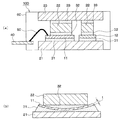
【解決手段】各半導体素子11、12と第1のリード21との間には、第1のはんだ31が介在しており、この第1のはんだ31を介して、各半導体素子11、12と第1のリード21とがはんだ接続され、各半導体素子11、12の上には、第2のはんだ32を介して、それぞれ第2の導体部材としてのターミナル22が搭載され、第2のはんだ32によりはんだ接続されており、第1のはんだ31の凝固点T1は第2のはんだ32の凝固点T2よりも低い。
【選択図】図1
Description
図8(a)は、本発明の他の実施形態にかかる半導体装置の要部の概略断面構成を示す図であり、図8(b)は(a)に示される構成の形成方法を示す概略断面図である。なお、この図8(a)において、図示しない部分は上記第1実施形態の半導体装置と同様である。
21…第1の導体部材としての第1のリード、21a…突起、
22…第2の導体部材としてのターミナル、
23…第3の導体部材としての第3のリード、
31…第1のはんだ、32…第2のはんだ、33…第3のはんだ。
Claims (4)
- 第1の導体部材(21)の上に第1のはんだ(31)を介して半導体素子(11、12)を搭載し、この半導体素子(11、12)の上に第2のはんだ(32)を介して第2の導体部材(22)を搭載した状態で、前記第1および第2のはんだ(31、32)をリフローさせることにより、前記半導体素子(11、12)と前記両導体部材(21、22)とをはんだ接続するようにした半導体装置において、
前記第1のはんだ(31)の凝固点が、前記第2のはんだ(32)の凝固点よりも低いことを特徴とする半導体装置。 - 前記半導体素子(11、12)の厚さは150μm以内であることを特徴とする請求項1に記載の半導体装置。
- 前記第2の導体部材(22)の上に第3のはんだ(33)を介して第3の導体部材(23)がはんだ接続されており、
前記第3のはんだ(33)の凝固点は、前記第1のはんだ(31)の凝固点および前記第2のはんだ(32)の凝固点よりも低いことを特徴とする請求項1または2に記載の半導体装置。 - 前記第1の導体部材(21)の上面のうち前記半導体素子(11、12)の端部が重なる部位には、突起(21a)が設けられていることを特徴とする請求項1ないし3のいずれか1つに記載の半導体装置。
Priority Applications (1)
| Application Number | Priority Date | Filing Date | Title |
|---|---|---|---|
| JP2006107161A JP4730181B2 (ja) | 2006-04-10 | 2006-04-10 | 半導体装置 |
Applications Claiming Priority (1)
| Application Number | Priority Date | Filing Date | Title |
|---|---|---|---|
| JP2006107161A JP4730181B2 (ja) | 2006-04-10 | 2006-04-10 | 半導体装置 |
Publications (2)
| Publication Number | Publication Date |
|---|---|
| JP2007281274A true JP2007281274A (ja) | 2007-10-25 |
| JP4730181B2 JP4730181B2 (ja) | 2011-07-20 |
Family
ID=38682405
Family Applications (1)
| Application Number | Title | Priority Date | Filing Date |
|---|---|---|---|
| JP2006107161A Expired - Fee Related JP4730181B2 (ja) | 2006-04-10 | 2006-04-10 | 半導体装置 |
Country Status (1)
| Country | Link |
|---|---|
| JP (1) | JP4730181B2 (ja) |
Cited By (8)
| Publication number | Priority date | Publication date | Assignee | Title |
|---|---|---|---|---|
| WO2010004609A1 (ja) * | 2008-07-07 | 2010-01-14 | 三菱電機株式会社 | 電力用半導体装置 |
| DE102009040444A1 (de) | 2009-03-23 | 2010-10-07 | Mitsubishi Electric Corp. | Leistungsmodul |
| JP2014135527A (ja) * | 2014-04-30 | 2014-07-24 | Rohm Co Ltd | 半導体パワーモジュールおよびその製造方法 |
| US8981542B2 (en) | 2010-09-29 | 2015-03-17 | Rohm Co., Ltd. | Semiconductor power module and method of manufacturing the same |
| JP2015095561A (ja) * | 2013-11-12 | 2015-05-18 | 株式会社デンソー | 半導体装置及びその製造方法 |
| JP2016219479A (ja) * | 2015-05-15 | 2016-12-22 | トヨタ自動車株式会社 | 半導体装置の製造方法及び半導体装置 |
| JP2018148169A (ja) * | 2017-03-09 | 2018-09-20 | トヨタ自動車株式会社 | 半導体装置 |
| EP3063697B1 (fr) * | 2013-10-30 | 2022-04-06 | Banks and Acquirers International Holding | Assemblage de lecture de carte à mémoire comprenant des protections anti-intrusion |
Families Citing this family (2)
| Publication number | Priority date | Publication date | Assignee | Title |
|---|---|---|---|---|
| JP6750263B2 (ja) | 2016-03-18 | 2020-09-02 | 富士電機株式会社 | 電力用半導体モジュール |
| JP7027751B2 (ja) | 2017-09-15 | 2022-03-02 | 富士電機株式会社 | 半導体モジュール |
Citations (3)
| Publication number | Priority date | Publication date | Assignee | Title |
|---|---|---|---|---|
| JPS52127160A (en) * | 1976-04-19 | 1977-10-25 | Toshiba Corp | Semiconductor device |
| JPH08139243A (ja) * | 1994-11-07 | 1996-05-31 | Rohm Co Ltd | 半導体装置の製造方法 |
| JP2001274177A (ja) * | 2000-03-24 | 2001-10-05 | Denso Corp | 半導体装置及びその製造方法 |
-
2006
- 2006-04-10 JP JP2006107161A patent/JP4730181B2/ja not_active Expired - Fee Related
Patent Citations (3)
| Publication number | Priority date | Publication date | Assignee | Title |
|---|---|---|---|---|
| JPS52127160A (en) * | 1976-04-19 | 1977-10-25 | Toshiba Corp | Semiconductor device |
| JPH08139243A (ja) * | 1994-11-07 | 1996-05-31 | Rohm Co Ltd | 半導体装置の製造方法 |
| JP2001274177A (ja) * | 2000-03-24 | 2001-10-05 | Denso Corp | 半導体装置及びその製造方法 |
Cited By (11)
| Publication number | Priority date | Publication date | Assignee | Title |
|---|---|---|---|---|
| WO2010004609A1 (ja) * | 2008-07-07 | 2010-01-14 | 三菱電機株式会社 | 電力用半導体装置 |
| JPWO2010004609A1 (ja) * | 2008-07-07 | 2011-12-22 | 三菱電機株式会社 | 電力用半導体装置 |
| DE102009040444A1 (de) | 2009-03-23 | 2010-10-07 | Mitsubishi Electric Corp. | Leistungsmodul |
| US7848104B2 (en) | 2009-03-23 | 2010-12-07 | Mitsubishi Electric Corporation | Power module |
| DE102009040444B4 (de) * | 2009-03-23 | 2012-11-08 | Mitsubishi Electric Corp. | Leistungsmodul |
| US8981542B2 (en) | 2010-09-29 | 2015-03-17 | Rohm Co., Ltd. | Semiconductor power module and method of manufacturing the same |
| EP3063697B1 (fr) * | 2013-10-30 | 2022-04-06 | Banks and Acquirers International Holding | Assemblage de lecture de carte à mémoire comprenant des protections anti-intrusion |
| JP2015095561A (ja) * | 2013-11-12 | 2015-05-18 | 株式会社デンソー | 半導体装置及びその製造方法 |
| JP2014135527A (ja) * | 2014-04-30 | 2014-07-24 | Rohm Co Ltd | 半導体パワーモジュールおよびその製造方法 |
| JP2016219479A (ja) * | 2015-05-15 | 2016-12-22 | トヨタ自動車株式会社 | 半導体装置の製造方法及び半導体装置 |
| JP2018148169A (ja) * | 2017-03-09 | 2018-09-20 | トヨタ自動車株式会社 | 半導体装置 |
Also Published As
| Publication number | Publication date |
|---|---|
| JP4730181B2 (ja) | 2011-07-20 |
Similar Documents
| Publication | Publication Date | Title |
|---|---|---|
| JP6206494B2 (ja) | 半導体装置 | |
| JP4302607B2 (ja) | 半導体装置 | |
| US11071212B2 (en) | Semiconductor device manufacturing method | |
| US20250183125A1 (en) | Electronic device and method for manufacturing electronic device | |
| JP4730181B2 (ja) | 半導体装置 | |
| US11164846B2 (en) | Semiconductor device manufacturing method and soldering support jig | |
| CN105518857B (zh) | 半导体装置、以及半导体装置的制造方法 | |
| JP5732880B2 (ja) | 半導体装置及びその製造方法 | |
| JP4228926B2 (ja) | 半導体装置 | |
| JP2005340268A (ja) | トランジスタパッケージ | |
| CN103201829B (zh) | 电路装置及其制造方法 | |
| JP6008750B2 (ja) | 半導体装置 | |
| CN102842555B (zh) | 半导体器件及其制造方法 | |
| JP2006190728A (ja) | 電力用半導体装置 | |
| JP2009147123A (ja) | 半導体装置及びその製造方法 | |
| JP7347047B2 (ja) | 半導体装置 | |
| JP4214880B2 (ja) | 半導体装置 | |
| JP4797492B2 (ja) | 半導体装置 | |
| JP4861200B2 (ja) | パワーモジュール | |
| JP4882394B2 (ja) | 半導体装置 | |
| JP2008270846A (ja) | 半導体装置の製造方法 | |
| JP2003133337A (ja) | 半導体実装構造および半導体実装方法 | |
| JP2014120717A (ja) | 電子装置およびその製造方法 | |
| JP2024174656A (ja) | 半導体装置および半導体装置の製造方法 | |
| JP2016030281A (ja) | 接合材料及び半導体装置 |
Legal Events
| Date | Code | Title | Description |
|---|---|---|---|
| A621 | Written request for application examination |
Free format text: JAPANESE INTERMEDIATE CODE: A621 Effective date: 20080512 |
|
| A977 | Report on retrieval |
Free format text: JAPANESE INTERMEDIATE CODE: A971007 Effective date: 20101224 |
|
| A131 | Notification of reasons for refusal |
Free format text: JAPANESE INTERMEDIATE CODE: A131 Effective date: 20110111 |
|
| A521 | Request for written amendment filed |
Free format text: JAPANESE INTERMEDIATE CODE: A523 Effective date: 20110301 |
|
| TRDD | Decision of grant or rejection written | ||
| A01 | Written decision to grant a patent or to grant a registration (utility model) |
Free format text: JAPANESE INTERMEDIATE CODE: A01 Effective date: 20110322 |
|
| A61 | First payment of annual fees (during grant procedure) |
Free format text: JAPANESE INTERMEDIATE CODE: A61 Effective date: 20110404 |
|
| FPAY | Renewal fee payment (event date is renewal date of database) |
Free format text: PAYMENT UNTIL: 20140428 Year of fee payment: 3 |
|
| R151 | Written notification of patent or utility model registration |
Ref document number: 4730181 Country of ref document: JP Free format text: JAPANESE INTERMEDIATE CODE: R151 |
|
| FPAY | Renewal fee payment (event date is renewal date of database) |
Free format text: PAYMENT UNTIL: 20140428 Year of fee payment: 3 |
|
| R250 | Receipt of annual fees |
Free format text: JAPANESE INTERMEDIATE CODE: R250 |
|
| R250 | Receipt of annual fees |
Free format text: JAPANESE INTERMEDIATE CODE: R250 |
|
| R250 | Receipt of annual fees |
Free format text: JAPANESE INTERMEDIATE CODE: R250 |
|
| R250 | Receipt of annual fees |
Free format text: JAPANESE INTERMEDIATE CODE: R250 |
|
| R250 | Receipt of annual fees |
Free format text: JAPANESE INTERMEDIATE CODE: R250 |
|
| R250 | Receipt of annual fees |
Free format text: JAPANESE INTERMEDIATE CODE: R250 |
|
| R250 | Receipt of annual fees |
Free format text: JAPANESE INTERMEDIATE CODE: R250 |
|
| R250 | Receipt of annual fees |
Free format text: JAPANESE INTERMEDIATE CODE: R250 |
|
| LAPS | Cancellation because of no payment of annual fees |