JP2007299534A - Transparent conductive film and touch panel using the same - Google Patents
Transparent conductive film and touch panel using the same Download PDFInfo
- Publication number
- JP2007299534A JP2007299534A JP2006123836A JP2006123836A JP2007299534A JP 2007299534 A JP2007299534 A JP 2007299534A JP 2006123836 A JP2006123836 A JP 2006123836A JP 2006123836 A JP2006123836 A JP 2006123836A JP 2007299534 A JP2007299534 A JP 2007299534A
- Authority
- JP
- Japan
- Prior art keywords
- refractive index
- transparent conductive
- layer
- film
- conductive film
- Prior art date
- Legal status (The legal status is an assumption and is not a legal conclusion. Google has not performed a legal analysis and makes no representation as to the accuracy of the status listed.)
- Pending
Links
Images


Landscapes
- Non-Insulated Conductors (AREA)
- Laminated Bodies (AREA)
- Position Input By Displaying (AREA)
Abstract
【課題】ニュートラルな反射・透過色調を実現する透明導電性フィルム及びこれを用いたタッチパネルを提供する。
【解決手段】透明フィルム104の一方の面に、酸素欠損金属酸化物層111、第1の高屈折率層112、第1の低屈折率層113、第2の高屈折率層114、第2の低屈折率層115、透明導電層116がこの順に積層された6層の積層膜が形成される。高透明で、ニュートラルな色調を有するタッチパネル用透明導電性フィルムが得られる。
【選択図】図1A transparent conductive film realizing a neutral reflection / transmission color tone and a touch panel using the transparent conductive film are provided.
An oxygen-deficient metal oxide layer, a first high-refractive index layer, a first low-refractive index layer, a second high-refractive index layer, and a second layer are formed on one surface of a transparent film. A six-layer film in which the low refractive index layer 115 and the transparent conductive layer 116 are laminated in this order is formed. A transparent conductive film for a touch panel having a highly transparent and neutral color tone can be obtained.
[Selection] Figure 1
Description
本発明は、表示装置の表示面上に設置されて使用される抵抗膜方式、静電容量方式などによるタッチパネルに用いて好適な透明導電性フィルム及びこれを用いたタッチパネルに関する。 The present invention relates to a transparent conductive film suitable for use in a touch panel by a resistive film system, a capacitive system, or the like that is used on a display surface of a display device, and a touch panel using the transparent conductive film.
近年、有機EL(エレクトロルミネッセンス)ディスプレイや液晶ディスプレイなどのディスプレイの表面に、ペン状の指示体又は指での押圧により情報を入力するパネルを設けるいわゆるタッチパネル(又はタッチスクリーン)が、電子手帳、携帯電話等の携帯端末や交通機関のチケット販売用入力機など、種々多様に使用されている。
一般に、タッチパネルの透明導電性フィルムに用いられる透明導電層は、屈折率が1.9から2.1程度であり、透明フィルムの屈折率1.45〜1.65に比べて高いことから、空気との界面において反射が発生し透過率が低下する。さらに透明導電層の反射率は波長依存性があることから、特定の波長の光の反射によって透明導電性フィルムが着色したように見え、有機ELディスプレイや液晶ディスプレイなどの表示装置の明るさや色調を損なうという問題がある。
In recent years, so-called touch panels (or touch screens) in which a panel for inputting information by pressing with a pen-shaped indicator or a finger is provided on the surface of a display such as an organic EL (electroluminescence) display or a liquid crystal display, are electronic notebooks, mobile phones, and the like. It is used in various ways, such as mobile terminals such as telephones and ticket sales input machines for transportation.
Generally, a transparent conductive layer used for a transparent conductive film of a touch panel has a refractive index of about 1.9 to 2.1 and is higher than the refractive index of 1.45 to 1.65 of a transparent film. Reflection occurs at the interface between the two and the transmittance decreases. Furthermore, since the reflectance of the transparent conductive layer is wavelength-dependent, the transparent conductive film appears to be colored by the reflection of light of a specific wavelength, and the brightness and color tone of display devices such as organic EL displays and liquid crystal displays can be adjusted. There is a problem of losing.
この問題の解決策として、透明基材と透明導電層の間に高屈折率層と低屈折率層を複数組み合わせることにより透過率を向上させようとする技術が提案されている(例えば特許文献1及び2参照。)。
また、透明フィルムの上に透過率の高い導電層を形成する技術も提案されている(例えば特許文献3参照。)。
As a solution to this problem, a technique for improving the transmittance by combining a plurality of high refractive index layers and low refractive index layers between a transparent substrate and a transparent conductive layer has been proposed (for example, Patent Document 1). And 2).
A technique for forming a conductive layer having a high transmittance on a transparent film has also been proposed (see, for example, Patent Document 3).
しかしながら、上記特許文献1及び2に開示の方法による場合は、透明基材としてガラス基板を使用しているため、ガラスよりも耐熱性が低く吸水性の高い透明フィルム上に同じ手法で形成しようとする場合、成膜中の熱によりフィルムがダメージを受けることや、フィルムのアウトガスにより透明導電膜の電気的特性が安定しないこと、またフィルムと積層膜の密着性が十分にとれないという問題点がある。
また、上記特許文献3に開示の方法では、可視領域の特定の波長に透過率のピークをもつ構造であるため、ある程度透過率の向上には寄与するものの、表示装置の表示波長領域全域にわたり高透過率を確保し、同時に、ニュートラルな反射・透過色調、すなわち特定の色が反射されないいわゆる無色透明の色調を両立させる技術は実現できていない。
すなわち、従来の透明導電性フィルムにおいては、透明導電層の屈折率が高いために、透過率の低下、反射の増大、色調の変化が発生することから、これを用いたタッチパネルにおいて、表示品質を著しく損なうという問題がある。
However, in the case of the methods disclosed in
Further, the method disclosed in
That is, in the conventional transparent conductive film, since the refractive index of the transparent conductive layer is high, the transmittance decreases, the reflection increases, and the color tone changes. There is a problem of significant damage.
上述の問題に鑑みて、本発明は、透過率を損なうことなく使用する光の波長領域にわたって反射率を抑え、ニュートラルな反射・透過色調を実現する透明導電性フィルム及びこれを用いたタッチパネルを提供することを目的とする。 In view of the above problems, the present invention provides a transparent conductive film that suppresses the reflectance over the wavelength region of light used without impairing the transmittance and realizes neutral reflection / transmission color tone, and a touch panel using the same. The purpose is to do.
上記課題を解決するため、本発明による透明導電性フィルムは、透明フィルムの一方の面に、酸素欠損金属酸化物層、第1の高屈折率層、第1の低屈折率層、第2の高屈折率層、第2の低屈折率層、透明導電層がこの順に積層された6層の積層膜が形成されて成る構成とする。 In order to solve the above-mentioned problems, the transparent conductive film according to the present invention has an oxygen deficient metal oxide layer, a first high refractive index layer, a first low refractive index layer, and a second layer on one surface of the transparent film. A six-layer film in which a high refractive index layer, a second low refractive index layer, and a transparent conductive layer are stacked in this order is formed.
上述の本発明構成の透明導電性フィルムによれば、高屈折率層と低屈折率層を順次積層しているため、界面における光干渉効果を利用して透過率を飛躍的に向上させることが可能であるとともに、反射率をより広い波長帯域において低下させることができるので、従来に比してよりニュートラルな反射・透過色調を実現することができる。 According to the transparent conductive film having the above-described configuration of the present invention, since the high refractive index layer and the low refractive index layer are sequentially laminated, the transmittance can be drastically improved by utilizing the optical interference effect at the interface. In addition, the reflectance can be lowered in a wider wavelength band, so that a more neutral reflection / transmission color tone can be realized as compared with the prior art.
本発明によれば、透過率を損なうことなく使用する光の波長領域にわたって反射率を抑え、ニュートラルな反射・透過色調を実現する透明導電性フィルム及びこれを用いたタッチパネルを提供することができる。 ADVANTAGE OF THE INVENTION According to this invention, a transparent conductive film which suppresses a reflectance over the wavelength range of the light to be used without impairing the transmittance, and realizes a neutral reflection / transmission color tone and a touch panel using the same can be provided.
以下本発明を実施するための最良の形態の例を説明するが、本発明は以下の例に限定されるものではない。
図1は、本発明の一実施形態例に係る透明導電性フィルム100の概略断面構成図である。図1に示すように、本発明の透明導電性フィルム100は、透明フィルム104の一方の面に、酸素欠損金属酸化物層111、第1の高屈折率層112、第1の低屈折率層113、第2の高屈折率層114、第2の低屈折率層115、透明導電層116がこの順に積層された6層の積層膜110が形成されて構成される。図示の例においては、透明フィルム基材101の両面にハードコート102及び103が形成されて透明フィルム104が構成された例を示す。
Examples of the best mode for carrying out the present invention will be described below, but the present invention is not limited to the following examples.
FIG. 1 is a schematic cross-sectional configuration diagram of a transparent
この場合、透明フィルム基材101の材料としては、表示装置の表示面上に設置するものとしての機能を満たすものであれば特に限定されることはないが、透明性、屈折率、分散、複屈折などの光学特性、さらには耐衝撃性、耐熱性、耐久性などの諸特性からみて、特にポリメチルメタアクリレート、メチルメタクリレートと他のアルキル(メタ)アクリレート、スチレンなどといったビニルモノマーとの共重合体などの(メタ)アクリル樹脂を用いることが可能である。また、ポリカーボネート、ジエチレングリコールビスアリルカーボネート(CR−39)などのポリカーボネート系樹脂を用いてもよい。更にまた、(臭素化)ビスフェノールA型のジ(メタ)アクリレートの単独重合体ないし共重合体、(臭素化)ビスフェノールA、モノ(メタ)アクリレートのウレタン変性モノマーの重合体及び共重合体などといった熱硬化性(メタ)アクリル系樹脂も適用可能である。その他、ポリエステル特にポリエチレンテレフタレート、ポリエチレンナフタレート及び不飽和ポリエステル、アクリロニトリル−スチレン共重合体、ポリ塩化ビニル、ポリウレタン、エポキシ樹脂、ポリアリレート、ポリエーテルスルホン、ポリエーテルケトン、シクロオレフィンポリマー、例えばアートン(JSR(株)製、登録商標)やゼオノア(日本ゼオン(株)製、登録商標)などを用いることが好ましい。また、耐熱性を考慮したアラミド系樹脂の使用も可能である。
In this case, the material of the
透明フィルム基材101はこれらの樹脂を延伸、あるいは溶剤に希釈後フィルム状に成膜して乾燥するなどの方法で得ることができ、厚さは通常25μm〜500μm程度であり、本発明の透明導電性フィルムに用いる場合も同様の厚さとすることができる。
またこの透明フィルム基材101は、その表面の表面エネルギー、塗布性、すべり性、平面性等を改善するために、表面処理として下塗り層を設ける場合がある。下塗り層はオルガノアルコキシメタル化合物やポリエステル、アクリル変性ポリエステル、ポリウレタンなどが挙げられる。また、コロナ放電、UV照射処理を行うことにより同様の効果を得る方法もある。
The
The
本例においては、この透明フィルム基材101の表面、図示の例ではその両面にハードコート102及び103を設ける構成とする。このように、表面にハードコートを設けることにより、透明フィルム基材101の表面の表面硬度、耐薬品性、耐擦傷性、耐久性の諸物性を向上させることが可能である。
ハードコート102及び103の材料としては、例えば特公昭50−28092号公報、特公昭50−28446号公報、特公昭51−24368号公報、特開昭52−112698号公報、特公昭57−2735号公報、特開2001−301095号公報に開示されているような、メチルトリエトキシシラン、フェニルトリエトキシシラン等のオルガノシラン系熱硬化型樹脂、エーテル化メチロールメラミン等のメラミン系熱硬化樹脂、ポリオールアクリレート、ポリエステルアクリレート、ウレタンアクリレート、エポキシアクリレート等の多官能アクリレート系紫外線硬化樹脂等より成る材料を用いることができる。また、必要に応じて特許3361857号公報、特開平11−140207号公報に開示されているように、微粒子を混合させた樹脂を用いることにより、有機ELパネル、液晶パネル等の表示装置の表示性能を損なわない程度の光散乱効果を持つものであってもよい。このハードコート102及び103の厚さとしては、通常1μm以上20μm以下程度とされ、本発明の透明導電性フィルムに用いる場合においても同様である。またハードコート102の表面をプラズマで処理することにより酸素欠損金属酸化物層111との密着性を向上させることが可能である。
In this example,
Examples of the material for the
酸素欠損金属酸化物層111は、ハードコート102とこの上の第1の高屈折率層112から透明導電層116に至る積層膜110との密着性を向上させる機能を有する。他にも、透明フィルム基材101、あるいはハードコート102の含有水分により透明導電膜116の抵抗値が経時変化することを防止する効果を持つ。酸素欠損金属酸化物層111はこのような機能を満たすものであればその製造方法に制限はないが、Arガス及び必要に応じて酸素ガス、二酸化炭素ガス、オゾンガス等を導入した減圧環境下においてSi、Ti、Cr等の金属陰極にDC(直流)又はAC(交流)電圧を印加することによりプラズマを発生させて成膜するマグネトロンスパッタ法により成膜することが最も好ましい。酸素欠損金属酸化物層111は、通常化学量論組成に比較して酸素量が20%〜80%にあることが望ましい。酸素欠損金属酸化物層の厚さは厚いほうが効果は上がるが、その一方で厚過ぎると透過率が下がるため、本発明においては1nm以上20nm以下の範囲、特に3nm以上5nm以下とすることが好ましい。
The oxygen-deficient
第1の高屈折率層112は、この上に形成される第1の低屈折率層113、第2の高屈折率層114、第2の低屈折率層115及び透明導電層116と共に、光干渉効果により透過率を向上させる他、透過と反射の色調をニュートラルにする効果を有する。第1の高屈折率層112の材料としては、目的とする波長帯域、すなわち可視光の波長帯域において透明であることが望ましい。また、この第1の高屈折率層112と第2の高屈折率層114の屈折率n(H)は、第1及び第2の低屈折率層113及び115の屈折率n(L)との比n(H)/n(L)が、
n(H)/n(L)≧1.4 ・・・(1)
であることが望ましい。これは、上述の光干渉効果を十分に得るためである。
この第1及び第2の高屈折率層112及び114の材料及び製造方法は上記式(1)を満たす材料及び製造方法であれば特に制限されるものではないが、Arガス及び必要に応じて酸素ガス、二酸化炭素ガス、オゾンガス等を導入した減圧環境下においてNb、Ti、Ta等を主成分とする金属あるいはセラミック陰極にDC又はAC電圧を印加することによりプラズマを発生させて成膜するマグネトロンスパッタ法により成膜することが最も好ましい。第1の高屈折率層112の光学膜厚nd1としては、上述の光干渉効果を良好に得て、かつ透過率の低下を回避するためには、20nm<nd1<70nmであればよく、35nm<nd1<55nmの範囲とすることがより好ましい。
The first high-
n (H) / n (L) ≧ 1.4 (1)
It is desirable that This is to sufficiently obtain the above-described optical interference effect.
The material and manufacturing method of the first and second high-refractive index layers 112 and 114 are not particularly limited as long as they are materials and manufacturing methods that satisfy the above formula (1). A magnetron that forms a film by generating a plasma by applying a DC or AC voltage to a metal or ceramic cathode containing Nb, Ti, Ta or the like as a main component in a reduced pressure environment in which oxygen gas, carbon dioxide gas, ozone gas, or the like is introduced. Most preferably, the film is formed by sputtering. The optical film thickness nd1 of the first high-
第1の低屈折率層113は、第1及び第2の高屈折率層112及び114、第2の低屈折率層115及び透明導電層116と共に、光干渉効果により透過率を向上させる他、透過と反射の色調をニュートラルにする効果を有する。第1の低屈折率層113の材料としては、透明であること及び第1及び第2の高屈折率層112及び114の屈折率と比較して、その比n(H)/n(L)が上記式(1)を満足するものであれば特に制限されるものではないが、Arガス及び必要に応じて酸素ガス、二酸化炭素ガス、オゾンガス等を導入した減圧環境下においてSiを主成分とする金属あるいはセラミック陰極にDC、AC又はRf(高周波)電圧を印加することによりプラズマを発生させて成膜するマグネトロンスパッタ法により成膜するのが最も好ましい。第1の低屈折率層113の光学膜厚nd2としては、上述の光干渉効果を良好に得て、かつ透過率の低下を回避するためには、10nm<nd2<90nmであればよく、20nm<nd2<40nmの範囲とすることがより好ましい。
The first low-
第2の高屈折率層114は、第1の高屈折率層112と第1及び第2の低屈折率層113及び115、透明導電層116と共に、光干渉効果により透過率を向上させる他、透過と反射の色調をニュートラルにする効果を有する。第2の高屈折率層114の材料及び製造方法としては、第1の高屈折率層112と同じ材料及び製造方法とすることが好ましい。第2の高屈折率層114の光学膜厚nd3としては、上述の光干渉効果を良好に得て、かつ透過率の低下を回避するためには、90nm<nd3<190nmであればよく、120nm<nd3<160nmの範囲とすることがより好ましい。
The second high-
第2の低屈折率層115は、第1及び第2の高屈折率層112及び114、第1の屈折率層113、透明導電層116と共に光干渉効果により透過率を向上させる他、透過と反射の色調をニュートラルにする効果を有する。第2の低屈折率層115の材料及び製造方法としては、第1の低屈折率層113と同じ材料及び製造方法とすることが好ましい。第2の低屈折率層115の光学膜厚nd4としては、上述の光干渉効果を良好に得て、かつ透過率の低下を回避するためには、40nm<nd4<120nmであればよく、60nm<nd4<100nmの範囲とすることがより好ましい。
The second low-
透明導電層116は、第1及び第2の高屈折率層及び低屈折率層112〜115と共に光干渉効果により透過率を向上させ、透過と反射の色調をニュートラルにする他、所定の電気抵抗を付与する効果を有する。この透明導電層116の材料としては、透明であることと屈折率が1.8以上2.1以下程度の範囲で所定の電気抵抗が得られれば特に制限されるものではないが、Arガス及び必要に応じて酸素ガス、二酸化炭素ガス、オゾンガス等を導入した減圧環境下においてITO(インジウム−スズ複合酸化物)を主成分とするセラミック陰極、ITを主成分とする金属陰極、Znを主成分とする金属あるいはセラミック陰極にDC、AC又はRf電圧を印加することによりプラズマを発生させて成膜するマグネトロンスパッタ法により成膜することが最も好ましい。透明導電層116の物理膜厚d5としては、十分な導電性、光干渉効果を得て、かつ透過率の低下を回避するためには、5nm<d5<80nmであればよく、10nm<d5<30nmの範囲とすることがより好ましい。
The transparent
図2は、上述した酸素欠損金属酸化物層111、第1の高屈折率層112、第1の低屈折率層113、第2の高屈折率層114、第2の低屈折率層115及び透明導電層116を透明フィルム104上に成膜するのに適したロール・ツー・ロールの真空スパッタ装置の一例の概略構成図である。図2に示すように、この真空スパッタ装置200には、中央部に冷却ドラム202が配置され、巻き出し機203から引き出された透明フィルム104はガイドロール214及び215を介して冷却ドラム202に巻きつけられ、ガイドロール216及び217を介して巻き取り機204に巻き取られる。図示の例では、巻き出し機203から冷却ドラム202に至る間のガイドロール214及び215間おいて、プラズマ処理部201が設けられる。また、冷却ドラム202の周囲には、第1〜第6の電極205〜210が冷却ドラム202に巻きつけられた透明フィルム104に対向して順に配置される。この第1〜第6の電極205〜210はそれぞれ、酸素欠損金属酸化物層成膜用、第1の高屈折率層成膜用、第1の低屈折率層成膜用、第2の高屈折率層成膜用、第2の低屈折率層成膜用、透明導電層成膜用として用いることができる。また、この真空スパッタ装置200には、例えば二つのガス導入口212及び213と真空ポンプ等の排気手段(図示せず)に連結される排気口211とが設けられ、矢印a3で示すように排気されて所定の真空度に保たれる。
このような装置200を用いて、プラズマ処理部201において透明フィルム104の表面をプラズマ処理した後、例えばガス導入口212及び213から矢印a1及びa2で示すようにArガス及び酸素ガス、また必要に応じてその他のガスを導入しながら、第1〜第6の電極にDC又はAC電圧を印加することによりプラズマを発生させて成膜するマグネトロンスパッタ法により図1に示す積層膜110の各層を連続的に成膜することができる。
2 shows the oxygen deficient
After plasma processing the surface of the
このようにして製造した本発明構成の透明導電性フィルムを用いてタッチパネルを構成し、表示装置上に配置した場合の概略構成図を図3に示す。この場合、図3に示すように、2枚の透明導電性フィルムを下部電極フィルム301及び上部電極フィルム302として、その透明導電層が形成された導電膜面が対向するように、スペーサ、図示の例ではドットスペーサ303を介して積層し、周囲を貼り合わせ材304で接着、粘着等により固定して、この場合抵抗膜式のタッチパネル300が構成される。また、図示しないが静電容量式タッチパネルの電極フィルムとしても使用することができる。
FIG. 3 shows a schematic configuration diagram when the touch panel is configured using the transparent conductive film of the present invention manufactured as described above and disposed on the display device. In this case, as shown in FIG. 3, the two transparent conductive films are used as the
次に、上述の図2に示す真空スパッタ装置を用いて実施例1及び比較例1〜5による透明導電性フィルムを作製し、その機械的特性(透明フィルムと積層膜との密着性)、電気的特性及び光学的特性について測定した結果について説明する。尚、本発明は以下に示す実施例1における構成に限定されるものではない。 Next, a transparent conductive film according to Example 1 and Comparative Examples 1 to 5 was prepared using the vacuum sputtering apparatus shown in FIG. 2 described above, and its mechanical properties (adhesion between the transparent film and the laminated film), electrical The measurement results of the optical characteristics and the optical characteristics will be described. In addition, this invention is not limited to the structure in Example 1 shown below.
〔1〕実施例1
この例においては、図1に示す透明フィルム基材101として、厚さ100μmのシクロオレフィンポリマー例えばゼオノア(日本ゼオン(株)製、登録商標)を用い、その両面に4μmの厚さでポリエステルアクリルレート系の樹脂を塗布した後UV乾燥炉で硬化させてハードコート102及び103を形成し、透明フィルム104を作製する。
次にこの透明フィルム104を図2において説明した真空スパッタ装置200にセットした後、真空ポンプ211で10−4Pa程度まで排気した後、Arガスを10−2Paまで導入する。
[1] Example 1
In this example, as the
Next, the
透明フィルム104を0.8m/分で走行させながら、プラズマ処理部201で透明フィルム104の表面を改質させた。第1の電極205(酸素欠損金属酸化物層成膜用)には金属Siを装着し、250kHzのAC電圧を印加してSiOx(x=1.0)膜を成膜した。印加電力はSiOx膜の物理膜厚が5nmになるように調整した。
第2の電極206(第1の高屈折率層成膜用)には金属Nbを装着し、Arガスと酸素ガスとの流量比(Ar/O2と記す)がAr/O2=2となるようにArガス及び酸素ガスを導入し、さらに250kHzのAC電圧を印加して第1の高屈折率層としてNb2O5膜を成膜した。このとき印加電力はNb2O5膜の光学膜厚が46nmになるよう調整した。
第3の電極207(第1の低屈折率層成膜用)には金属Siを装着し、Ar/O2=3となるように酸素ガスを導入し、さらに250kHzのAC電圧を印加してSiO2膜を成膜した。印加電力はSiO2膜の光学膜厚が29nmになるよう調整した。
第4の電極208(第2の高屈折率層成膜用)には金属Nbを装着し、Ar/O2=2となるように酸素ガスを導入し、さらに250kHzのAC電圧を印加してNb2O5膜を成膜した。印加電力はNb2O5膜の光学膜厚が139nmになるように調整した。
第5の電極209(第2の低屈折率層成膜用)には金属Siを装着し、Ar/O2=3となるように酸素ガスを導入し、さらに250kHzのAC電圧を印加してSiO2膜を成膜した。印加電力はSiO2膜の光学膜厚が80nmになるように調整した。
第6の電極210(透明導電層成膜用)にはITOを装着し、Arの1.0%程度の流量の酸素ガスを導入し、さらに250kHzのAC電圧を印加してITO膜を成膜した。印加電力はITO膜の表面抵抗が500Ω/sqになるよう調整したところ、ITOの物理膜厚は15nmであった。この場合の各層の材料、屈折率、物理膜厚、光学膜厚を以下の表1に示す。
While the
The second electrode 206 (for the first high refractive index layer deposition) fitted with a metal Nb, flow ratio of Ar gas and oxygen gas (referred to as Ar / O 2) is the
The third electrode 207 (for forming the first low refractive index layer) is provided with metal Si, oxygen gas is introduced so that Ar / O 2 = 3, and an AC voltage of 250 kHz is applied. A SiO 2 film was formed. The applied power was adjusted so that the optical film thickness of the SiO 2 film was 29 nm.
A metal Nb is attached to the fourth electrode 208 (for forming the second high refractive index layer), oxygen gas is introduced so that Ar / O 2 = 2, and an AC voltage of 250 kHz is applied. An Nb 2 O 5 film was formed. The applied power was adjusted so that the optical film thickness of the Nb 2 O 5 film was 139 nm.
The fifth electrode 209 (for forming the second low-refractive index layer) is provided with metal Si, oxygen gas is introduced so that Ar / O 2 = 3, and an AC voltage of 250 kHz is applied. It was a SiO 2 film. The applied power was adjusted so that the optical film thickness of the SiO 2 film was 80 nm.
ITO is attached to the sixth electrode 210 (for forming a transparent conductive layer), oxygen gas having a flow rate of about 1.0% of Ar is introduced, and an AC voltage of 250 kHz is further applied to form an ITO film. did. When the applied power was adjusted so that the surface resistance of the ITO film was 500 Ω / sq, the physical film thickness of ITO was 15 nm. The material, refractive index, physical film thickness, and optical film thickness of each layer in this case are shown in Table 1 below.

〔2〕比較例1
上述の実施例1における酸素欠損金属酸化物層としてのSiOx層をなくした他は、上記実施例1と同様の構成とした。この場合の各層の材料、屈折率、物理膜厚、光学膜厚を以下の表2に示す。
[2] Comparative Example 1
The configuration was the same as in Example 1 except that the SiOx layer as the oxygen-deficient metal oxide layer in Example 1 was eliminated. The material, refractive index, physical film thickness, and optical film thickness of each layer in this case are shown in Table 2 below.
〔3〕比較例2
上述の実施例1における酸素欠損金属酸化物層の成膜時に、Arガスと酸素がストの流量比がAr/O2=2となるように酸素ガスを導入することにより、SiOx(x=1.0)ではなくSiO2膜として構成した。SiO2膜の物理膜厚が5nmになるよう印加電力を調整した。この場合の各層の材料、屈折率、物理膜厚、光学膜厚を以下の表3に示す。
[3] Comparative Example 2
When forming the oxygen-deficient metal oxide layer in Example 1 described above, by introducing oxygen gas so that the flow rate ratio of Ar gas to oxygen strikes Ar / O 2 = 2, SiOx (x = 1) .0), not SiO 2 film. The applied power was adjusted so that the physical film thickness of the SiO 2 film was 5 nm. The material, refractive index, physical film thickness, and optical film thickness of each layer in this case are shown in Table 3 below.
〔4〕比較例3
上述の実施例1において、6層構成ではなく、下記の表4に示すように、高屈折率層及び低屈折率層をそれぞれ1層とする4層構成とし、透過率のピークが550nmとなるようにその膜厚を調整して構成した。この場合の各層の材料、屈折率、物理膜厚、光学膜厚を以下の表4に示す。
[4] Comparative Example 3
In Example 1 described above, instead of a 6-layer structure, as shown in Table 4 below, a high-refractive index layer and a low-refractive index layer are each formed into a 4-layer structure, and the transmittance peak is 550 nm. In this way, the film thickness was adjusted. The material, refractive index, physical film thickness, and optical film thickness of each layer in this case are shown in Table 4 below.
〔5〕比較例4
上述の比較例3と同様に、下記の表5に示すように、高屈折率層及び低屈折率層をそれぞれ1層とする4層構成とし、透過率のピークが450nmとなるように構成した。この場合の各層の材料、屈折率、物理膜厚、光学膜厚を以下の表5に示す。
[5] Comparative Example 4
Similar to Comparative Example 3 described above, as shown in Table 5 below, a high-refractive-index layer and a low-refractive-index layer were each composed of four layers, and the transmittance peak was 450 nm. . The material, refractive index, physical film thickness, and optical film thickness of each layer in this case are shown in Table 5 below.
〔6〕比較例5
上述の実施例1における第2及び第4の電極206及び208に金属Siを装着し、O2の代わりにN2ガスを導入し、さらに250kHzのAC電圧を印加してSiN膜を成膜した。この場合、高屈折率層と低屈折率層との屈折率比はn(H)/n(L)=1.34となっている。印加電力は第1の高屈折率層の光学膜厚が39nm、第2の高屈折率層の光学膜厚が137nmとなるように調整した。さらに、第1の低屈折率層の光学膜厚を44nmとすることにより色調を最適化した。この場合の各層の材料、屈折率、物理膜厚、光学膜厚を以下の表6に示す。
[6] Comparative Example 5
Metal Si was attached to the second and
このようにして作製した実施例1及び比較例1〜5による透明導電性フィルムについて、機械特性及び電気特性を測定した結果を下記の表7に示し、また光学特性を調べた結果を表8、図4及び図5に示す。機械特性についてはJIS K5600に準じた碁盤目剥離試験を行い、積層膜と透明フィルムとの密着性について調べた。試料25個中剥離の生じなかった個数を示す。電気特性については4端子プローブ(三菱化学(株)のロレスタMCP−T360、商品名)で評価した。光学特性のうち反射特性についてはフィルムの裏面に黒テープを貼ることにより裏面反射の影響を除去して分光光度計(V−560、JASCO Inc.社製、商品名)で測定した。 About the transparent conductive film by Example 1 and Comparative Examples 1-5 produced in this way, the result of having measured the mechanical property and the electrical property is shown in the following Table 7, and the result of examining the optical property is shown in Table 8, It shows in FIG.4 and FIG.5. As for the mechanical properties, a cross-cut peel test according to JIS K5600 was conducted to examine the adhesion between the laminated film and the transparent film. The number in which no peeling occurred in 25 samples is shown. The electrical characteristics were evaluated with a 4-terminal probe (Loresta MCP-T360, trade name, manufactured by Mitsubishi Chemical Corporation). Of the optical properties, the reflection property was measured with a spectrophotometer (V-560, product name, manufactured by JASCO Inc.) after removing the influence of back surface reflection by applying a black tape to the back surface of the film.
表7は実施例1と比較例1及び2における機械特性と電気特性の違いを示したものである。比較例1では実施例1と比べ酸素欠損金属酸化物層がないため、特に、温度60℃湿度90%24時間の高温高湿試験後の密着性が悪く、剥離の生じない試料は見られなかった。また、同様の高温高湿試験後の電気抵抗についても大幅に増大し、安定しないことが分かる。比較例2では酸素欠損金属酸化物層ではなく完全な酸化物層で代用したものである。この場合でも高温高湿試験後の密着性が悪い他、電気抵抗も安定しないことが分かる。
したがって、透明フィルムと第1の高屈折率層との間に酸素欠損金属酸化物層を設けない場合、また、酸素欠損金属酸化物層に換えて金属酸化物層を設ける場合においては、機械特性及び電気特性において劣化が見られることがわかる。
Table 7 shows the difference in mechanical properties and electrical properties between Example 1 and Comparative Examples 1 and 2. Since Comparative Example 1 does not have an oxygen-deficient metal oxide layer as compared with Example 1, in particular, no adhesion was observed after a high-temperature and high-humidity test at a temperature of 60 ° C. and a humidity of 90% for 24 hours, and no sample was observed. It was. It can also be seen that the electrical resistance after the same high-temperature and high-humidity test greatly increases and is not stable. In Comparative Example 2, a complete oxide layer is used instead of the oxygen-deficient metal oxide layer. Even in this case, it is understood that the adhesion after the high temperature and high humidity test is not good and the electric resistance is not stable.
Therefore, when no oxygen-deficient metal oxide layer is provided between the transparent film and the first high refractive index layer, or when a metal oxide layer is provided instead of the oxygen-deficient metal oxide layer, mechanical properties are It can also be seen that the electrical characteristics are degraded.
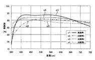
表8、図4及び5は実施例と比較例3〜5の光学特性の違いを示したものである。図4及図5から、実施例1においては可視光域とりわけ表示体の表示域において94%程度の高透過率が得られ、また表示装置の表示域である波長450nm以上600nm以下の波長帯域において低反射率であることが分かる。
また、表8から明らかなように、L*a*b*表色系(1976年国際照明委員会(CIE)で規格化、JIS(JISZ8729))のL*a*b*色空間で定義される(a*,b*)において、透過色調は、(a*)2+(b*)2=0.17であることから、
(a*)2+(b*)2≦1 ・・・(2)
を満たし、反射色調は、(a*)2+(b*)2=89.91であり、
(a*)2+(b*)2≦100・・・(3)
を満たし、ニュートラルな透過・反射色調を維持しているため、表示装置の前面に配置しても表示特性にほとんど影響を与えないことが分かる。
また、液晶ディスプレイにおいては、その色再現性を評価する上で透過色調の色温度は最も重要な数値であり、6450K以上6550以下であることが望ましい。表8より、実施例においては透過色調の色温度は6544Kであることから、この透明導電性フィルムは、液晶ディスプレイに用いる場合に好適であることが分かる。
Table 8, FIGS. 4 and 5 show the difference in optical characteristics between the examples and the comparative examples 3 to 5. 4 and 5, in Example 1, a high transmittance of about 94% is obtained in the visible light region, particularly in the display region of the display body, and in the wavelength range of 450 nm to 600 nm which is the display region of the display device. It can be seen that the reflectance is low.
As is clear from Table 8, it is defined in the L * a * b * color space of the L * a * b * color system (standardized by the International Commission on Illumination (CIE) in 1976, JIS (JISZ8729)). that (a *, b *) in the transmission color tone, because it is (a *) 2 + (b *) 2 = 0.17,
(A * ) 2 + (b * ) 2 ≦ 1 (2)
And the reflection color tone is (a * ) 2 + (b * ) 2 = 89.91,
(A * ) 2 + (b * ) 2 ≦ 100 (3)
Since the neutral transmission / reflection color tone is satisfied, it can be seen that even if it is arranged on the front surface of the display device, the display characteristics are hardly affected.
Further, in the liquid crystal display, the color temperature of the transmitted color tone is the most important numerical value for evaluating the color reproducibility, and is desirably 6450K or more and 6550 or less. From Table 8, it can be seen that the transparent conductive film is suitable for use in a liquid crystal display since the color temperature of the transmitted color tone is 6544 K in the examples.
これに対し、比較例3では積層数を減らしているため、図4及び図5に示すように、光干渉効果を最大限利用しても全波長帯域で反射率が比較的高く、また透過率が低い。更に、表8に示すように、透過色は黄色く、反射色は強い赤紫色になる。この場合、L*a*b*色空間で定義される(a*,b*)において、透過色調は、
(a*)2+(b*)2=4.10>1
となり、反射色調においても、
(a*)2+(b*)2=406.93>100
となってしまい、上記式(2)及び(3)を満たさない。このようなフィルムを表示装置の前面に設置した場合色調が変化してしまうため好ましくない。
また、透過色調の色温度も6408Kとなり、液晶ディスプレイに用いる透明導電性フィルムとしては不適切であることが分かる。
On the other hand, since the number of stacked layers is reduced in Comparative Example 3, as shown in FIGS. 4 and 5, even if the optical interference effect is used to the maximum, the reflectance is relatively high in all wavelength bands, and the transmittance is also high. Is low. Furthermore, as shown in Table 8, the transmitted color is yellow and the reflected color is a strong red-purple color. In this case, in (a * , b * ) defined in the L * a * b * color space, the transmission color tone is
(A * ) 2 + (b * ) 2 = 4.10> 1
In the reflection color tone,
(A *) 2 + (b *) 2 = 406.93> 100
Thus, the above formulas (2) and (3) are not satisfied. When such a film is installed on the front surface of the display device, the color tone changes, which is not preferable.
In addition, the color temperature of the transmitted color tone is 6408K, which proves inappropriate as a transparent conductive film used for a liquid crystal display.
また比較例4は、比較例3の構成で膜厚を調整することにより、透過色調を重視した例である。図4及び図5に示すように、透過率は低下してしまい、反射率は波長帯域によって高くなり、表8に示すように、透過色調こそ薄い青色であるが、反射色調は強い黄色となってしまう。この場合、L*a*b*色空間で定義される(a*,b*)において、透過色調は、
(a*)2+(b*)2=1.01>1
となり、反射色調においても、
(a*)2+(b*)2=160.73>100
となってしまい、上記式(2)及び(3)を満たさない。このようなフィルムを表示装置の全面に設置した場合、透過は暗く、反射は黄色くなるので好ましくない。
透過色調の色温度も6607Kであり、比較例3と同様に、液晶ディスプレイに用いる場合には適さないことが分かる。
Comparative Example 4 is an example in which the transmission color tone is emphasized by adjusting the film thickness with the configuration of Comparative Example 3. As shown in FIG. 4 and FIG. 5, the transmittance decreases and the reflectance increases depending on the wavelength band. As shown in Table 8, the transmitted color tone is light blue, but the reflected color tone is strong yellow. End up. In this case, in (a * , b * ) defined in the L * a * b * color space, the transmission color tone is
(A *) 2 + (b *) 2 = 1.01> 1
In the reflection color tone,
(A * ) 2 + (b * ) 2 = 160.73> 100
Thus, the above formulas (2) and (3) are not satisfied. When such a film is installed on the entire surface of the display device, transmission is dark and reflection is yellow, which is not preferable.
The color temperature of the transmission color tone is also 6607 K, and it can be seen that, similarly to Comparative Example 3, it is not suitable for use in a liquid crystal display.
比較例5では高屈折率材料としてNb2O5(n=2.32)ではなくSiN(n=1.95)を使用している、従って高屈折率膜と低屈折率膜の比をn(H)/n(L)=1.59から1.34にしたものである。積層数は同じであるため表示装置の表示域である450nm以上600nm以下の波長帯域において、図4及び図5に示すようにフラットな透過及び反射特性実現しているものの、屈折率比が低いため光干渉効果を十分活かすことができず、透過率が下がり、反射率がやや上昇する。表8に示すように、上記式(2)及び(3)は満たしており、また、透過色調の色温度は6482Kであって液晶ディスプレイに適用可能な範囲ではあるものの、全光線透過率(JIS K7361)は93%未満となってしまう。このようなフィルムを表示装置の前面に設置した場合、表示面が暗くなってしまうため好ましくない。
したがって、本発明の透明導電性フィルムにおいては、上述の構成とすることにより全光線透過率(JIS K7361)が93%以上であり、かつその色調が上記式(2)及び(3)を満たし、良好な光学特性を得ることができることが分かる。また透過色調の色温度が液晶ディスプレイに用いる場合に最適な範囲であることが分かる。
In Comparative Example 5, SiN (n = 1.95) is used as the high refractive index material instead of Nb 2 O 5 (n = 2.32). Therefore, the ratio of the high refractive index film to the low refractive index film is set to n. (H) / n (L) = 1.59 to 1.34. Since the number of layers is the same, flat transmission and reflection characteristics are realized as shown in FIGS. 4 and 5 in the wavelength band of 450 nm to 600 nm, which is the display area of the display device, but the refractive index ratio is low. The light interference effect cannot be fully utilized, the transmittance is lowered, and the reflectance is slightly increased. As shown in Table 8, the above formulas (2) and (3) are satisfied, and the color temperature of the transmission color tone is 6482K, which is within the range applicable to the liquid crystal display, but the total light transmittance (JIS). K7361) is less than 93%. When such a film is installed on the front surface of the display device, the display surface becomes dark, which is not preferable.
Therefore, in the transparent conductive film of the present invention, the total light transmittance (JIS K7361) is 93% or more by the above-described configuration, and the color tone satisfies the above formulas (2) and (3), It can be seen that good optical properties can be obtained. It can also be seen that the color temperature of the transmitted color tone is in the optimum range when used in a liquid crystal display.
以上の結果から明らかなように、本発明構成の透明導電性フィルムによれば、2層の高屈折率層と低屈折率層を交互に積層しているため、界面における光干渉効果を利用して透過率を飛躍的に向上させることが可能であるとともに、さらに透明フィルム基材の上に酸素欠損金属酸化物層を介して積層するため、タッチパネル用透明導電フィルムに要求される、強い機械特性と、安定した電気抵抗特性を得ることが可能である。
また本発明の透明導電性フィルムを抵抗膜式タッチパネル、静電容量式タッチパネルに適用することで、表示装置の表示性能を損なうことなく、実用的に十分な機械特性と電気特性を有するタッチパネルを得ることができる。
As is clear from the above results, according to the transparent conductive film of the configuration of the present invention, since the two high refractive index layers and low refractive index layers are alternately laminated, the light interference effect at the interface is utilized. It is possible to drastically improve the transmittance, and furthermore, because it is laminated on the transparent film substrate via an oxygen-deficient metal oxide layer, strong mechanical properties required for transparent conductive films for touch panels Thus, stable electric resistance characteristics can be obtained.
Further, by applying the transparent conductive film of the present invention to a resistive touch panel and a capacitive touch panel, a touch panel having practically sufficient mechanical and electrical characteristics can be obtained without impairing the display performance of the display device. be able to.
特に、本発明の透明導電性フィルムにおいて、第1及び第2の高屈折率層の屈折率n(H)と、第1及び第2の低屈折率層の屈折率n(L)の屈折率比n(H)/n(L)を1.4以上とすることによって、上述の光干渉効果を確実に得ることができ、可視光の広い領域に渡り高い透過率と低反射を実現することが可能である。
また、本発明の透明導電性フィルムの表面抵抗値として200Ω/sq以上10kΩ/sq以下とすることによって、抵抗膜式タッチパネル及び静電容量式タッチパネルとしては実用上適切な表面抵抗値とし、良好な電気特性とすることができる。
また更に、本発明の透明導電性フィルムにおいて、全光線透過率(JIS K7361)が93%以上であり、かつその色調が、CIE(1976)L*a*b*色空間で定義される(a*,b*)において、透過色調及び反射色調を、上記式(2)及び(3)を満たす範囲とすることによって、確実に可視域、特に表示体の表示波長域において高透過及びニュートラルな透過・反射色調を実現できるため、タッチパネルに用いた場合においても表示装置の色調を損なわない、光学特性に優れた透明導電性フィルムを得ることが可能である。
In particular, in the transparent conductive film of the present invention, the refractive index n (H) of the first and second high refractive index layers and the refractive index n (L) of the first and second low refractive index layers. By setting the ratio n (H) / n (L) to 1.4 or more, the above-described optical interference effect can be obtained reliably, and high transmittance and low reflection can be realized over a wide area of visible light. Is possible.
In addition, by setting the surface resistance value of the transparent conductive film of the present invention to 200 Ω / sq or more and 10 kΩ / sq or less, the surface resistance value suitable for practical use as a resistive film type touch panel and a capacitance type touch panel is obtained. It can be electrical characteristics.
Furthermore, in the transparent conductive film of the present invention, the total light transmittance (JIS K7361) is 93% or more, and the color tone is defined by CIE (1976) L * a * b * color space (a * , B * ), the transmission color tone and the reflection color tone are within the range satisfying the above formulas (2) and (3), thereby ensuring high transmission and neutral transmission in the visible range, particularly in the display wavelength range of the display body. -Since a reflective color tone can be realized, it is possible to obtain a transparent conductive film excellent in optical characteristics that does not impair the color tone of a display device even when used for a touch panel.
更に、本発明の透明導電性フィルムにおいて、第1及び第2の高屈折率層をNb2O5又はTiO2より構成し、第1及び第2の低屈折率層をSiO2より構成し、透明導電層をITO又はZnを主成分とする合金酸化物より構成し、また酸素欠損金属酸化物層を、Si、Ti、Crを主成分とする酸素欠損金属酸化物より構成することによって、確実に、機械特性、抵抗安定性、高い透過率とニュートラルな色調をもつ透明導電性フィルムを得ることが可能である。
また、本発明の透明導電性フィルムにおいて、透明フィルムを冷却させながら、6層の積層膜をロール・ツー・ロールのスパッタ法で製造することによって、耐熱性の低いフィルム基材上にも、透明導電性フィルムを容易に量産することが可能である。
Furthermore, in the transparent conductive film of the present invention, the first and second high refractive index layers are composed of Nb 2 O 5 or TiO 2 , and the first and second low refractive index layers are composed of SiO 2 , The transparent conductive layer is made of an alloy oxide containing ITO or Zn as a main component, and the oxygen deficient metal oxide layer is made of an oxygen deficient metal oxide containing Si, Ti, or Cr as main components. In addition, it is possible to obtain a transparent conductive film having mechanical properties, resistance stability, high transmittance, and neutral color tone.
In addition, in the transparent conductive film of the present invention, a transparent film is cooled, and a six-layer laminated film is produced by a roll-to-roll sputtering method, so that it is transparent even on a film substrate having low heat resistance. It is possible to easily mass-produce the conductive film.
なお、本発明は、上述の各例において説明した材料及び構成に限定されるものではなく、本発明構成を逸脱しない範囲において種々の変形、変更が可能であることはいうまでもない。 In addition, this invention is not limited to the material and structure demonstrated in each above-mentioned example, It cannot be overemphasized that a various deformation | transformation and change are possible in the range which does not deviate from this invention structure.
100.透明導電性フィルム、101.透明フィルム基材、102.ハードコート、103.ハードコート、104.透明フィルム、110.積層膜、111.酸素欠損金属酸化物層、112.第1の高屈折率層、113.第1の低屈折率層、114.第2の高屈折率層、115.第2の高屈折率層、116.透明導電層、200.真空スパッタ装置、201.プラズマ処理部、202.冷却ドラム、203.巻き出し機、204.巻き取り機、205.第1の電極、206.第2の電極、207.第3の電極、208.第4の電極、209.第5の電極、210.第6の電極、211.排気口、212.ガス導入口、213.ガス導入口、214〜217.ガイドロール、300.タッチパネル、301.下部電極フィルム、302.上部電極フィルム、303.ドットスペーサ、304.貼り合わせ材、307.基材、308.液晶パネル、309.バックライト、310.表示装置
100. 101. transparent conductive film Transparent film substrate, 102. Hard coat, 103. Hard coat, 104. Transparent film, 110. Laminated film, 111. Oxygen deficient metal oxide layer, 112. First high-refractive-index layer, 113. First low refractive index layer, 114. Second high refractive index layer, 115. Second high refractive index layer, 116. Transparent conductive layer, 200. 201. Vacuum sputtering apparatus. Plasma processing unit, 202. Cooling drum, 203. Unwinding machine, 204. Winding machine, 205. First electrode, 206. Second electrode, 207. Third electrode, 208.
Claims (10)
ことを特徴とする透明導電性フィルム。 On one surface of the transparent film, an oxygen-deficient metal oxide layer, a first high refractive index layer, a first low refractive index layer, a second high refractive index layer, a second low refractive index layer, a transparent conductive layer A transparent conductive film characterized in that a six-layered film is formed by laminating layers in this order.
(a*)2+(b*)2≦1
を満たし、反射色調は、
(a*)2+(b*)2≦100
を満たすことを特徴とする請求項1記載の透明導電性フィルム。 Total light transmittance (JIS K7361) is not less than 93%, and its color tone, CIE1976 (JIS Z 8729) of the L * a * b * defined in the color space (a *, b *) in the transmission color Is
(A * ) 2 + (b * ) 2 ≦ 1
And the reflection color tone is
(A * ) 2 + (b * ) 2 ≦ 100
The transparent conductive film according to claim 1, wherein:
前記上部電極フィルム及び/又は下部電極フィルムは、
透明フィルムの一方の面に、酸素欠損金属酸化物層、第1の高屈折率層、第1の低屈折率層、第2の高屈折率層、第2の低屈折率層、透明導電層がこの順に積層された6層の積層膜が形成されて成る
ことを特徴とするタッチパネル。 A touch panel that is disposed on a display surface of a display device and is formed by laminating an upper electrode film and a lower electrode film while maintaining a predetermined interval,
The upper electrode film and / or the lower electrode film is
On one surface of the transparent film, an oxygen-deficient metal oxide layer, a first high refractive index layer, a first low refractive index layer, a second high refractive index layer, a second low refractive index layer, a transparent conductive layer A touch panel characterized by comprising a laminated film of 6 layers laminated in this order.
Priority Applications (1)
| Application Number | Priority Date | Filing Date | Title |
|---|---|---|---|
| JP2006123836A JP2007299534A (en) | 2006-04-27 | 2006-04-27 | Transparent conductive film and touch panel using the same |
Applications Claiming Priority (1)
| Application Number | Priority Date | Filing Date | Title |
|---|---|---|---|
| JP2006123836A JP2007299534A (en) | 2006-04-27 | 2006-04-27 | Transparent conductive film and touch panel using the same |
Publications (1)
| Publication Number | Publication Date |
|---|---|
| JP2007299534A true JP2007299534A (en) | 2007-11-15 |
Family
ID=38768869
Family Applications (1)
| Application Number | Title | Priority Date | Filing Date |
|---|---|---|---|
| JP2006123836A Pending JP2007299534A (en) | 2006-04-27 | 2006-04-27 | Transparent conductive film and touch panel using the same |
Country Status (1)
| Country | Link |
|---|---|
| JP (1) | JP2007299534A (en) |
Cited By (18)
| Publication number | Priority date | Publication date | Assignee | Title |
|---|---|---|---|---|
| JP2010152809A (en) * | 2008-12-26 | 2010-07-08 | Smk Corp | Transparent panel body and touch panel |
| JP2010182562A (en) * | 2009-02-06 | 2010-08-19 | Toppan Printing Co Ltd | Transparent conductive film |
| JP2010182472A (en) * | 2009-02-04 | 2010-08-19 | Toppan Printing Co Ltd | Transparent conductive film |
| JP2010186642A (en) * | 2009-02-12 | 2010-08-26 | Hitachi Maxell Ltd | Transparent conductive sheet and method of manufacturing the same |
| JP2011145593A (en) * | 2010-01-18 | 2011-07-28 | Nippon Zeon Co Ltd | Hard coat film and image display element |
| JP2012020425A (en) * | 2010-07-12 | 2012-02-02 | Tdk Corp | Transparent conductor and touch panel using the same |
| JP2012118936A (en) * | 2010-12-03 | 2012-06-21 | Dainippon Printing Co Ltd | Touch panel sensor with transparent sheet |
| JP2012206307A (en) * | 2011-03-29 | 2012-10-25 | Toppan Printing Co Ltd | Transparent conductive laminate and touch panel using the same |
| CN103337279A (en) * | 2013-06-26 | 2013-10-02 | 汕头万顺包装材料股份有限公司光电薄膜分公司 | Transparent conductive film and touch panel employing same |
| JP2014146365A (en) * | 2009-03-31 | 2014-08-14 | Dainippon Printing Co Ltd | Touch panel sensor, laminated body for creating touch panel sensor, and method for manufacturing touch panel sensor |
| JP2014525069A (en) * | 2012-05-14 | 2014-09-25 | ナンチャン オー−フィルム テック カンパニー リミテッド | A new process for manufacturing double-sided conductive films. |
| CN104882495A (en) * | 2015-05-07 | 2015-09-02 | 厦门神科太阳能有限公司 | Transparent conductive window layer for solar cell, and CIGS-base thin-film solar cell |
| US9189033B2 (en) | 2010-09-29 | 2015-11-17 | Dai Nippon Printing Co., Ltd. | Touchscreen panel sensor film and manufacturing method thereof |
| WO2016052158A1 (en) * | 2014-09-29 | 2016-04-07 | コニカミノルタ株式会社 | Transparent conductor and touch panel including same |
| JP2016162454A (en) * | 2015-02-27 | 2016-09-05 | ティーピーケイ タッチ ソリューションズ(シアメン)インコーポレーテッド | Touch panel |
| CN110042359A (en) * | 2019-05-14 | 2019-07-23 | 南京汇金锦元光电材料有限公司 | Flexible transparent electromagnetic shielding film and preparation method |
| JP2020134752A (en) * | 2019-02-21 | 2020-08-31 | 三菱電機株式会社 | Liquid crystal display device |
| CN115893866A (en) * | 2022-10-28 | 2023-04-04 | 四川旭虹光电科技有限公司 | A method and system for continuously preparing AG film, AR film and AF film |
Citations (4)
| Publication number | Priority date | Publication date | Assignee | Title |
|---|---|---|---|---|
| JP2003004902A (en) * | 2001-06-14 | 2003-01-08 | Applied Vacuum Coating Technologies Co Ltd | Antireflective conductive multilayered thin film having transparent conductive film as outermost layer |
| JP2003080624A (en) * | 2001-09-07 | 2003-03-19 | Nof Corp | Transparent conductive material and touch panel |
| JP2003255104A (en) * | 2002-03-05 | 2003-09-10 | Dainippon Printing Co Ltd | Transparent laminated film and method for producing the same |
| JP2004021550A (en) * | 2002-06-14 | 2004-01-22 | Sony Corp | Touch panel, display, anti-reflection film, and method for producing these |
-
2006
- 2006-04-27 JP JP2006123836A patent/JP2007299534A/en active Pending
Patent Citations (4)
| Publication number | Priority date | Publication date | Assignee | Title |
|---|---|---|---|---|
| JP2003004902A (en) * | 2001-06-14 | 2003-01-08 | Applied Vacuum Coating Technologies Co Ltd | Antireflective conductive multilayered thin film having transparent conductive film as outermost layer |
| JP2003080624A (en) * | 2001-09-07 | 2003-03-19 | Nof Corp | Transparent conductive material and touch panel |
| JP2003255104A (en) * | 2002-03-05 | 2003-09-10 | Dainippon Printing Co Ltd | Transparent laminated film and method for producing the same |
| JP2004021550A (en) * | 2002-06-14 | 2004-01-22 | Sony Corp | Touch panel, display, anti-reflection film, and method for producing these |
Cited By (19)
| Publication number | Priority date | Publication date | Assignee | Title |
|---|---|---|---|---|
| JP2010152809A (en) * | 2008-12-26 | 2010-07-08 | Smk Corp | Transparent panel body and touch panel |
| JP2010182472A (en) * | 2009-02-04 | 2010-08-19 | Toppan Printing Co Ltd | Transparent conductive film |
| JP2010182562A (en) * | 2009-02-06 | 2010-08-19 | Toppan Printing Co Ltd | Transparent conductive film |
| JP2010186642A (en) * | 2009-02-12 | 2010-08-26 | Hitachi Maxell Ltd | Transparent conductive sheet and method of manufacturing the same |
| JP2014146365A (en) * | 2009-03-31 | 2014-08-14 | Dainippon Printing Co Ltd | Touch panel sensor, laminated body for creating touch panel sensor, and method for manufacturing touch panel sensor |
| JP2011145593A (en) * | 2010-01-18 | 2011-07-28 | Nippon Zeon Co Ltd | Hard coat film and image display element |
| JP2012020425A (en) * | 2010-07-12 | 2012-02-02 | Tdk Corp | Transparent conductor and touch panel using the same |
| US9189033B2 (en) | 2010-09-29 | 2015-11-17 | Dai Nippon Printing Co., Ltd. | Touchscreen panel sensor film and manufacturing method thereof |
| JP2012118936A (en) * | 2010-12-03 | 2012-06-21 | Dainippon Printing Co Ltd | Touch panel sensor with transparent sheet |
| JP2012206307A (en) * | 2011-03-29 | 2012-10-25 | Toppan Printing Co Ltd | Transparent conductive laminate and touch panel using the same |
| JP2014525069A (en) * | 2012-05-14 | 2014-09-25 | ナンチャン オー−フィルム テック カンパニー リミテッド | A new process for manufacturing double-sided conductive films. |
| CN103337279A (en) * | 2013-06-26 | 2013-10-02 | 汕头万顺包装材料股份有限公司光电薄膜分公司 | Transparent conductive film and touch panel employing same |
| WO2016052158A1 (en) * | 2014-09-29 | 2016-04-07 | コニカミノルタ株式会社 | Transparent conductor and touch panel including same |
| JP2016162454A (en) * | 2015-02-27 | 2016-09-05 | ティーピーケイ タッチ ソリューションズ(シアメン)インコーポレーテッド | Touch panel |
| CN104882495A (en) * | 2015-05-07 | 2015-09-02 | 厦门神科太阳能有限公司 | Transparent conductive window layer for solar cell, and CIGS-base thin-film solar cell |
| CN104882495B (en) * | 2015-05-07 | 2017-01-11 | 厦门神科太阳能有限公司 | Transparent conductive window layer for solar cell, and CIGS-base thin-film solar cell |
| JP2020134752A (en) * | 2019-02-21 | 2020-08-31 | 三菱電機株式会社 | Liquid crystal display device |
| CN110042359A (en) * | 2019-05-14 | 2019-07-23 | 南京汇金锦元光电材料有限公司 | Flexible transparent electromagnetic shielding film and preparation method |
| CN115893866A (en) * | 2022-10-28 | 2023-04-04 | 四川旭虹光电科技有限公司 | A method and system for continuously preparing AG film, AR film and AF film |
Similar Documents
| Publication | Publication Date | Title |
|---|---|---|
| JP2007299534A (en) | Transparent conductive film and touch panel using the same | |
| CN113728251B (en) | Optical laminate and article | |
| US9860981B2 (en) | Transparent conductive film and method for producing same | |
| KR100779441B1 (en) | Transparent conductive laminate | |
| JP5803062B2 (en) | Transparent conductor and touch panel using the same | |
| US20120057237A1 (en) | Electrode film and coordinate detecting apparatus | |
| JP5692859B2 (en) | Transparent conductive laminated film, method for producing the same, and touch panel including the same | |
| KR102155622B1 (en) | Hard coat film and its application | |
| WO2006028131A9 (en) | Touch panel and method for manufacturing film material for touch panel | |
| JP5958476B2 (en) | Transparent conductor and touch panel | |
| CN107533402B (en) | Transparent conductor, method for manufacturing same, and touch panel | |
| JP2011167914A (en) | Laminated film and transparent conductive laminated film using the same, transparent conductive laminated sheet and touch panel | |
| US6235398B1 (en) | Transparent laminate and filter for plasma display panel using the transparent laminate | |
| JP5297125B2 (en) | Gas barrier film with transparent conductive film and touch panel using the same | |
| CN106132686B (en) | Laminated body, transparent conductive laminate and touch panel | |
| JP2004214069A (en) | Transparent conductive film, transparent conductive laminate, and touch panel | |
| CN104641332A (en) | Transparent conductive film, manufacturing method of transparent conductive film, and touch panel | |
| US20070281178A1 (en) | PDP filter having multi-layer thin film and method of manufacturing the same | |
| EP4254022A1 (en) | Optical laminate and article | |
| JP2000147245A (en) | Optical filter | |
| KR102887447B1 (en) | Optical laminates and articles | |
| JP5463680B2 (en) | Transparent conductive film | |
| JP2024048953A (en) | Anti-reflection film, its manufacturing method, and image display device | |
| JP2013174787A (en) | Optical member | |
| US12619009B2 (en) | Optical laminate and article |
Legal Events
| Date | Code | Title | Description |
|---|---|---|---|
| A621 | Written request for application examination |
Free format text: JAPANESE INTERMEDIATE CODE: A621 Effective date: 20090424 |
|
| A977 | Report on retrieval |
Free format text: JAPANESE INTERMEDIATE CODE: A971007 Effective date: 20110228 |
|
| A131 | Notification of reasons for refusal |
Free format text: JAPANESE INTERMEDIATE CODE: A131 Effective date: 20110315 |
|
| A521 | Written amendment |
Free format text: JAPANESE INTERMEDIATE CODE: A523 Effective date: 20110509 |
|
| A02 | Decision of refusal |
Free format text: JAPANESE INTERMEDIATE CODE: A02 Effective date: 20110816 |