JP2007335441A - 静電破壊保護装置 - Google Patents
静電破壊保護装置 Download PDFInfo
- Publication number
- JP2007335441A JP2007335441A JP2006162002A JP2006162002A JP2007335441A JP 2007335441 A JP2007335441 A JP 2007335441A JP 2006162002 A JP2006162002 A JP 2006162002A JP 2006162002 A JP2006162002 A JP 2006162002A JP 2007335441 A JP2007335441 A JP 2007335441A
- Authority
- JP
- Japan
- Prior art keywords
- terminal
- voltage
- region
- electrostatic breakdown
- breakdown protection
- Prior art date
- Legal status (The legal status is an assumption and is not a legal conclusion. Google has not performed a legal analysis and makes no representation as to the accuracy of the status listed.)
- Granted
Links
Images









Classifications
-
- H—ELECTRICITY
- H10—SEMICONDUCTOR DEVICES; ELECTRIC SOLID-STATE DEVICES NOT OTHERWISE PROVIDED FOR
- H10D—INORGANIC ELECTRIC SEMICONDUCTOR DEVICES
- H10D8/00—Diodes
- H10D8/80—PNPN diodes, e.g. Shockley diodes or break-over diodes
-
- H—ELECTRICITY
- H10—SEMICONDUCTOR DEVICES; ELECTRIC SOLID-STATE DEVICES NOT OTHERWISE PROVIDED FOR
- H10D—INORGANIC ELECTRIC SEMICONDUCTOR DEVICES
- H10D8/00—Diodes
- H10D8/01—Manufacture or treatment
- H10D8/041—Manufacture or treatment of multilayer diodes
-
- H—ELECTRICITY
- H10—SEMICONDUCTOR DEVICES; ELECTRIC SOLID-STATE DEVICES NOT OTHERWISE PROVIDED FOR
- H10D—INORGANIC ELECTRIC SEMICONDUCTOR DEVICES
- H10D89/00—Aspects of integrated devices not covered by groups H10D84/00 - H10D88/00
- H10D89/60—Integrated devices comprising arrangements for electrical or thermal protection, e.g. protection circuits against electrostatic discharge [ESD]
- H10D89/601—Integrated devices comprising arrangements for electrical or thermal protection, e.g. protection circuits against electrostatic discharge [ESD] for devices having insulated gate electrodes, e.g. for IGFETs or IGBTs
- H10D89/711—Integrated devices comprising arrangements for electrical or thermal protection, e.g. protection circuits against electrostatic discharge [ESD] for devices having insulated gate electrodes, e.g. for IGFETs or IGBTs using bipolar transistors as protective elements
- H10D89/713—Integrated devices comprising arrangements for electrical or thermal protection, e.g. protection circuits against electrostatic discharge [ESD] for devices having insulated gate electrodes, e.g. for IGFETs or IGBTs using bipolar transistors as protective elements including a PNP transistor and a NPN transistor, wherein each of said transistors has its base region coupled to the collector region of the other transistor, e.g. silicon controlled rectifier [SCR] devices
-
- H—ELECTRICITY
- H10—SEMICONDUCTOR DEVICES; ELECTRIC SOLID-STATE DEVICES NOT OTHERWISE PROVIDED FOR
- H10D—INORGANIC ELECTRIC SEMICONDUCTOR DEVICES
- H10D62/00—Semiconductor bodies, or regions thereof, of devices having potential barriers
- H10D62/10—Shapes, relative sizes or dispositions of the regions of the semiconductor bodies; Shapes of the semiconductor bodies
- H10D62/102—Constructional design considerations for preventing surface leakage or controlling electric field concentration
- H10D62/103—Constructional design considerations for preventing surface leakage or controlling electric field concentration for increasing or controlling the breakdown voltage of reverse-biased devices
- H10D62/105—Constructional design considerations for preventing surface leakage or controlling electric field concentration for increasing or controlling the breakdown voltage of reverse-biased devices by having particular doping profiles, shapes or arrangements of PN junctions; by having supplementary regions, e.g. junction termination extension [JTE]
- H10D62/108—Constructional design considerations for preventing surface leakage or controlling electric field concentration for increasing or controlling the breakdown voltage of reverse-biased devices by having particular doping profiles, shapes or arrangements of PN junctions; by having supplementary regions, e.g. junction termination extension [JTE] having localised breakdown regions, e.g. built-in avalanching regions
-
- H—ELECTRICITY
- H10—SEMICONDUCTOR DEVICES; ELECTRIC SOLID-STATE DEVICES NOT OTHERWISE PROVIDED FOR
- H10W—GENERIC PACKAGES, INTERCONNECTIONS, CONNECTORS OR OTHER CONSTRUCTIONAL DETAILS OF DEVICES COVERED BY CLASS H10
- H10W42/00—Arrangements for protection of devices
- H10W42/80—Arrangements for protection of devices protecting against overcurrent or overload, e.g. fuses or shunts
Landscapes
- Semiconductor Integrated Circuits (AREA)
- Metal-Oxide And Bipolar Metal-Oxide Semiconductor Integrated Circuits (AREA)
- Bipolar Integrated Circuits (AREA)
Abstract
【解決手段】静電破壊保護回路は、第1の電源端子、第2の電源端子及び入出力端子を有する半導体装置の静電破壊保護装置であって、前記入力端子から前記第2の電源端子にサージ電流を流すサイリスタと、前記第1の電源端子から前記入力端子にサージ電流を流すバイポーラトランジスタとを有する。
【選択図】図6
Description
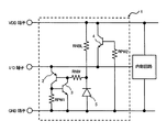
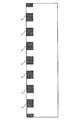
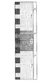
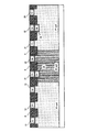
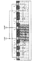
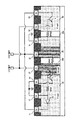
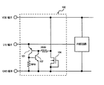
以下、図面を参照して本発明の実施の形態について説明する。実施の形態1にかかる静電破壊保護装置の回路図を図1に示す。図1に示すように、実施の形態1にかかる静電破壊保護装置1は、PNPトランジスタ(第2のバイポーラトランジスタ)2、NPNトランジスタ(第3のバイポーラトランジスタ)3、NPNトランジスタ(第1のバイポーラトランジスタ)4及びダイオード(トリガ素子)5を有している。また、静電破壊保護装置1は、第1の電源端子(以降、VDD端子と称す)、入出力端子(以降、I/O端子と称す)、第2の電源端子(以降、GND端子と称す)を有している。I/O端子は、半導体装置の内部回路と接続されている。内部回路は、例えばNMOSトランジスタとPMOSトランジスタとを用いた回路である。
また、NPNトランジスタ4のエミッタ端子の電圧は、接地電圧となり、ベース端子の電圧は接地電圧となるため、NPNトランジスタ3も動作しない。
NPNトランジスタ4のエミッタ端子の電圧は電源電圧となり、ベース端子の電圧は接地電圧となるため、NPNトランジスタ4も動作しない。
2 PNPトランジスタ
3、4 NPNトランジスタ
5 ダイオード
6 絶縁領域
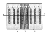
10、30、34a Pウェル領域
20、23a Nウェル領域
11 カソード領域
12 アノード領域
13、21、32 エミッタ領域
22、31 ベース領域
24 ディープNウェル領域
33 コレクタ領域
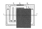
41 層間膜
42 コンタクト
43 金属配線
44 層間膜
45 ビア
46 金属配線
RPW、RNW 抵抗
Claims (10)
- 第1の電源端子、第2の電源端子及び入出力端子を有する半導体装置の静電破壊保護装置であって、
前記入出力端子から前記第2の電源端子にサージ電流を流すサイリスタと、
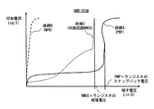
前記第1の電源端子から前記入出力端子にサージ電流を流すバイポーラトランジスタとを有する静電破壊保護回路。 - 前記サイリスタがターンオン状態となる電圧は、前記バイポーラトランジスタに形成された寄生ダイオードのブレークダウン電圧よりも低い電圧であることを特徴とする請求項1に記載の静電破壊保護回路。
- 前記バイポーラトランジスタのコレクタ−エミッタ間が導通状態となる電圧は、前記サイリスタ内に形成された寄生ダイオードのブレークダウン電圧よりも低い電圧であることを特徴とする請求項1あるいは2に記載の静電破壊保護回路。
- 第1の電源端子に一方の端子が接続され、入出力端子に他方の端子が接続され、第2の電源端子に制御端子が接続された第1のバイポーラトランジスタと、
前記入出力端子に一方の端子が接続され、前記第2の電源端子に他方の端子が接続され、前記第1の電源端子に制御端子が接続されたサイリスタとを有する静電破壊保護回路。 - 前記サイリスタは、
前記入出力端子に一方の端子が接続され、前記第2の電源端子に他方の端子が接続され、トリガ素子及び前記第1の電源端子に制御端子が接続された第2のバイポーラトランジスタと、
前記第2の電源端子に一方の端子が接続され、前記第1のバイポーラトランジスタの制御端子に他方の端子が接続され、前記第2の電源端子に制御端子が接続された第3のバイポーラトランジスタとを有することを特徴とする請求項4に記載の静電破壊保護回路。 - 前記サイリスタがターンオン状態となる電圧は、前記第1のバイポーラトランジスタに形成された寄生ダイオードのブレークダウン電圧よりも低い電圧であることを特徴とする請求項4あるいは5に記載の静電破壊保護回路。
- 前記第1のバイポーラトランジスタのコレクタ−エミッタ間が導通状態となる電圧は、前記サイリスタ内に形成された寄生ダイオードのブレークダウン電圧よりも低い電圧であることを特徴とする請求項4乃至6のいずれか1項に記載の静電破壊保護回路。
- 前記第1のバイポーラトランジスタは、第1導電型のウェル内に形成され、当該第1のバイポーラトランジスタの前記入出力端子に接続される他方の端子部に、第2導電型の第1の拡散部と、第1の拡散部とは異なる不純物濃度の第2導電型の第2の拡散部とを有することを特徴とする請求項4乃至7のいずれか1項に記載の静電破壊保護回路。
- 前記第2のバイポーラトランジスタは、第2導電型のウェル内に形成され、当該第2のバイポーラトランジスタの前記入出力端子に接続される他方の端子部に、第1導電型の第3の拡散部と、第3の拡散部とは異なる不純物濃度の第1導電型の第4の拡散部とを有することを特徴とする請求項4乃至8のいずれか1項に記載の静電破壊保護回路。
- 第1の端子から第2の端子に向かって順方向電流を流すPN接合部と、
前記第1、第2の端子間に接続され、前記PN接合部の降伏電圧よりも低い電圧でターンオン状態となるサイリスタとを有する静電破壊保護回路。
Priority Applications (3)
| Application Number | Priority Date | Filing Date | Title |
|---|---|---|---|
| JP2006162002A JP4209433B2 (ja) | 2006-06-12 | 2006-06-12 | 静電破壊保護装置 |
| US11/806,962 US8107203B2 (en) | 2006-06-12 | 2007-06-05 | Electrostatic discharge protection device |
| CN200710109034.4A CN101097916B (zh) | 2006-06-12 | 2007-06-12 | 静电放电保护器件 |
Applications Claiming Priority (1)
| Application Number | Priority Date | Filing Date | Title |
|---|---|---|---|
| JP2006162002A JP4209433B2 (ja) | 2006-06-12 | 2006-06-12 | 静電破壊保護装置 |
Publications (2)
| Publication Number | Publication Date |
|---|---|
| JP2007335441A true JP2007335441A (ja) | 2007-12-27 |
| JP4209433B2 JP4209433B2 (ja) | 2009-01-14 |
Family
ID=38821023
Family Applications (1)
| Application Number | Title | Priority Date | Filing Date |
|---|---|---|---|
| JP2006162002A Expired - Fee Related JP4209433B2 (ja) | 2006-06-12 | 2006-06-12 | 静電破壊保護装置 |
Country Status (3)
| Country | Link |
|---|---|
| US (1) | US8107203B2 (ja) |
| JP (1) | JP4209433B2 (ja) |
| CN (1) | CN101097916B (ja) |
Cited By (1)
| Publication number | Priority date | Publication date | Assignee | Title |
|---|---|---|---|---|
| WO2025263408A1 (ja) * | 2024-06-19 | 2025-12-26 | ローム株式会社 | 半導体モジュールおよび通信装置 |
Families Citing this family (13)
| Publication number | Priority date | Publication date | Assignee | Title |
|---|---|---|---|---|
| FR2904473B1 (fr) * | 2006-07-27 | 2009-01-16 | St Microelectronics Sa | Dispositif de protection d'un circuit integre contre les decharges electrostatiques |
| EP2572381A1 (en) * | 2010-05-18 | 2013-03-27 | Freescale Semiconductor, Inc. | Integrated circuit, electronic device and esd protection therefor |
| KR101847227B1 (ko) * | 2013-05-31 | 2018-04-10 | 매그나칩 반도체 유한회사 | Esd 트랜지스터 |
| KR101975608B1 (ko) * | 2013-06-12 | 2019-05-08 | 매그나칩 반도체 유한회사 | 고전압용 esd 트랜지스터 및 그 정전기 보호 회로 |
| WO2015056040A1 (en) * | 2013-10-18 | 2015-04-23 | Freescale Semiconductor, Inc. | Electrostatic discharge protection device structures and methods of manufacture |
| US9793258B1 (en) | 2016-11-04 | 2017-10-17 | United Microelectronics Corp. | Electrostatic discharge device |
| US10361186B1 (en) * | 2018-02-07 | 2019-07-23 | Infineon Technologies Ag | Suppression of parasitic discharge path in an electrical circuit |
| KR102781988B1 (ko) | 2018-12-17 | 2025-03-18 | 에스케이하이닉스 주식회사 | Esd 보호 장치 |
| DE102019108334A1 (de) * | 2019-03-29 | 2020-10-01 | X-Fab Semiconductor Foundries Gmbh | ESD-Schutzbauelement und MOS-Transistor mit (zumindest) einem integrierten ESD-Schutzbauelement |
| US11282831B2 (en) * | 2019-09-18 | 2022-03-22 | Taiwan Semiconductor Manufacturing Co., Ltd. | Semiconductor device having multiple electrostatic discharge (ESD) paths |
| US12349470B2 (en) | 2019-09-18 | 2025-07-01 | Taiwan Semiconductor Manufacturing Co., Ltd. | Semiconductor device having multiple electrostatic discharge (ESD) paths |
| CN115621275A (zh) * | 2021-07-16 | 2023-01-17 | 长鑫存储技术有限公司 | 静电保护电路及半导体器件 |
| US20230020459A1 (en) * | 2021-07-16 | 2023-01-19 | Changxin Memory Technologies, Inc. | Electro-static discharge protection circuit and semiconductor device |
Family Cites Families (12)
| Publication number | Priority date | Publication date | Assignee | Title |
|---|---|---|---|---|
| US3914749A (en) * | 1974-12-23 | 1975-10-21 | Ibm | D.C. stable single device memory cell |
| JPS58225663A (ja) * | 1982-06-23 | 1983-12-27 | Toshiba Corp | 半導体装置の製造方法 |
| JP2549726B2 (ja) * | 1989-01-30 | 1996-10-30 | 株式会社東芝 | 半導体集積回路とその製造方法 |
| US5705841A (en) * | 1995-12-22 | 1998-01-06 | Winbond Electronics Corporation | Electrostatic discharge protection device for integrated circuits and its method for fabrication |
| US5808342A (en) * | 1996-09-26 | 1998-09-15 | Texas Instruments Incorporated | Bipolar SCR triggering for ESD protection of high speed bipolar/BiCMOS circuits |
| JP3244065B2 (ja) * | 1998-10-23 | 2002-01-07 | 日本電気株式会社 | 半導体静電保護素子及びその製造方法 |
| KR100281908B1 (ko) * | 1998-11-20 | 2001-02-15 | 김덕중 | 반도체소자 및 그 제조방법 |
| JP3983067B2 (ja) | 2001-03-19 | 2007-09-26 | Necエレクトロニクス株式会社 | 半導体集積回路の静電保護回路 |
| DE102004009981B4 (de) * | 2004-03-01 | 2005-12-29 | Infineon Technologies Ag | ESD-Schutzschaltkreis mit Kollektorstrom-gesteuerter Zündung für eine monolithisch integrierte Schaltung |
| JP4437682B2 (ja) | 2004-03-17 | 2010-03-24 | 日本電信電話株式会社 | 低容量esd保護回路 |
| US7242561B2 (en) * | 2005-01-12 | 2007-07-10 | Silicon Integrated System Corp. | ESD protection unit with ability to enhance trigger-on speed of low voltage triggered PNP |
| US7304334B2 (en) * | 2005-09-16 | 2007-12-04 | Cree, Inc. | Silicon carbide bipolar junction transistors having epitaxial base regions and multilayer emitters and methods of fabricating the same |
-
2006
- 2006-06-12 JP JP2006162002A patent/JP4209433B2/ja not_active Expired - Fee Related
-
2007
- 2007-06-05 US US11/806,962 patent/US8107203B2/en not_active Expired - Fee Related
- 2007-06-12 CN CN200710109034.4A patent/CN101097916B/zh not_active Expired - Fee Related
Cited By (1)
| Publication number | Priority date | Publication date | Assignee | Title |
|---|---|---|---|---|
| WO2025263408A1 (ja) * | 2024-06-19 | 2025-12-26 | ローム株式会社 | 半導体モジュールおよび通信装置 |
Also Published As
| Publication number | Publication date |
|---|---|
| CN101097916B (zh) | 2011-04-27 |
| JP4209433B2 (ja) | 2009-01-14 |
| US20070284665A1 (en) | 2007-12-13 |
| CN101097916A (zh) | 2008-01-02 |
| US8107203B2 (en) | 2012-01-31 |
Similar Documents
| Publication | Publication Date | Title |
|---|---|---|
| CN101097915B (zh) | 用于半导体器件的静电放电保护方法及器件 | |
| US8107203B2 (en) | Electrostatic discharge protection device | |
| JP2009060117A (ja) | 半導体回路構造のesd保護の効果を改良するための方法および回路構造 | |
| JP2006319330A (ja) | 静電気放電保護装置 | |
| JP2011066246A (ja) | 静電気保護用半導体装置 | |
| JP2010182727A (ja) | 半導体装置 | |
| JP2009239050A (ja) | 保護回路 | |
| KR20090098237A (ko) | 높은 홀딩 전압을 갖는 스택형 실리콘 제어 정류기를구비한 정전기 방전 보호소자 | |
| JP5203850B2 (ja) | 静電気保護素子 | |
| JP6007606B2 (ja) | 半導体装置 | |
| CN103077945B (zh) | 半导体装置 | |
| JP5529414B2 (ja) | 静電破壊保護回路 | |
| JP5529436B2 (ja) | 静電破壊保護回路 | |
| JP2006278911A (ja) | 静電保護回路及び該静電保護回路を含む半導体装置 | |
| KR20240133029A (ko) | Esd 보호 소자 및 그 제조방법 | |
| JP7257982B2 (ja) | 半導体装置 | |
| JP2005235844A (ja) | 半導体装置 | |
| TWI553820B (zh) | 半導體裝置 | |
| JP2005317874A (ja) | Mosトランジスタおよびこれを備えた半導体集積回路装置 | |
| JP2009038101A (ja) | 半導体装置 | |
| US7656009B2 (en) | Robust ESD cell | |
| TWI440157B (zh) | 高電壓靜電放電防護用之自我檢測裝置及其製造方法 | |
| JP2012028380A (ja) | 半導体装置 | |
| KR20010029964A (ko) | 반도체 집적회로용 입출력 보호 장치 | |
| JP2010182821A (ja) | 半導体装置 |
Legal Events
| Date | Code | Title | Description |
|---|---|---|---|
| A977 | Report on retrieval |
Free format text: JAPANESE INTERMEDIATE CODE: A971007 Effective date: 20080414 |
|
| A131 | Notification of reasons for refusal |
Free format text: JAPANESE INTERMEDIATE CODE: A131 Effective date: 20080422 |
|
| A521 | Request for written amendment filed |
Free format text: JAPANESE INTERMEDIATE CODE: A523 Effective date: 20080619 |
|
| A131 | Notification of reasons for refusal |
Free format text: JAPANESE INTERMEDIATE CODE: A131 Effective date: 20080715 |
|
| A521 | Request for written amendment filed |
Free format text: JAPANESE INTERMEDIATE CODE: A523 Effective date: 20080825 |
|
| TRDD | Decision of grant or rejection written | ||
| A01 | Written decision to grant a patent or to grant a registration (utility model) |
Free format text: JAPANESE INTERMEDIATE CODE: A01 Effective date: 20080924 |
|
| A01 | Written decision to grant a patent or to grant a registration (utility model) |
Free format text: JAPANESE INTERMEDIATE CODE: A01 |
|
| A61 | First payment of annual fees (during grant procedure) |
Free format text: JAPANESE INTERMEDIATE CODE: A61 Effective date: 20081022 |
|
| R150 | Certificate of patent or registration of utility model |
Free format text: JAPANESE INTERMEDIATE CODE: R150 |
|
| FPAY | Renewal fee payment (event date is renewal date of database) |
Free format text: PAYMENT UNTIL: 20111031 Year of fee payment: 3 |
|
| FPAY | Renewal fee payment (event date is renewal date of database) |
Free format text: PAYMENT UNTIL: 20111031 Year of fee payment: 3 |
|
| S533 | Written request for registration of change of name |
Free format text: JAPANESE INTERMEDIATE CODE: R313533 |
|
| FPAY | Renewal fee payment (event date is renewal date of database) |
Free format text: PAYMENT UNTIL: 20111031 Year of fee payment: 3 |
|
| R350 | Written notification of registration of transfer |
Free format text: JAPANESE INTERMEDIATE CODE: R350 |
|
| FPAY | Renewal fee payment (event date is renewal date of database) |
Free format text: PAYMENT UNTIL: 20111031 Year of fee payment: 3 |
|
| FPAY | Renewal fee payment (event date is renewal date of database) |
Free format text: PAYMENT UNTIL: 20121031 Year of fee payment: 4 |
|
| FPAY | Renewal fee payment (event date is renewal date of database) |
Free format text: PAYMENT UNTIL: 20121031 Year of fee payment: 4 |
|
| FPAY | Renewal fee payment (event date is renewal date of database) |
Free format text: PAYMENT UNTIL: 20131031 Year of fee payment: 5 |
|
| LAPS | Cancellation because of no payment of annual fees |