JP2008016169A - Semiconductor memory device and driving method thereof - Google Patents
Semiconductor memory device and driving method thereof Download PDFInfo
- Publication number
- JP2008016169A JP2008016169A JP2007050765A JP2007050765A JP2008016169A JP 2008016169 A JP2008016169 A JP 2008016169A JP 2007050765 A JP2007050765 A JP 2007050765A JP 2007050765 A JP2007050765 A JP 2007050765A JP 2008016169 A JP2008016169 A JP 2008016169A
- Authority
- JP
- Japan
- Prior art keywords
- signal
- sense amplifier
- bit line
- amplifier enable
- write
- Prior art date
- Legal status (The legal status is an assumption and is not a legal conclusion. Google has not performed a legal analysis and makes no representation as to the accuracy of the status listed.)
- Pending
Links
- 239000004065 semiconductor Substances 0.000 title claims abstract description 36
- 238000000034 method Methods 0.000 title claims abstract description 15
- 230000004044 response Effects 0.000 claims abstract description 41
- 230000003321 amplification Effects 0.000 claims description 17
- 238000003199 nucleic acid amplification method Methods 0.000 claims description 17
- 230000008878 coupling Effects 0.000 claims description 3
- 238000010168 coupling process Methods 0.000 claims description 3
- 238000005859 coupling reaction Methods 0.000 claims description 3
- 230000000630 rising effect Effects 0.000 claims description 3
- 238000003491 array Methods 0.000 description 7
- 238000010586 diagram Methods 0.000 description 7
- 239000000872 buffer Substances 0.000 description 4
- 230000007274 generation of a signal involved in cell-cell signaling Effects 0.000 description 4
- 238000000926 separation method Methods 0.000 description 4
- 239000003990 capacitor Substances 0.000 description 3
- 238000011084 recovery Methods 0.000 description 3
- 230000001934 delay Effects 0.000 description 2
- 230000008569 process Effects 0.000 description 2
- 238000004904 shortening Methods 0.000 description 2
- 230000004913 activation Effects 0.000 description 1
- 230000008859 change Effects 0.000 description 1
- 230000000694 effects Effects 0.000 description 1
- 230000010354 integration Effects 0.000 description 1
- 238000012986 modification Methods 0.000 description 1
- 230000004048 modification Effects 0.000 description 1
Images




Classifications
-
- G—PHYSICS
- G11—INFORMATION STORAGE
- G11C—STATIC STORES
- G11C7/00—Arrangements for writing information into, or reading information out from, a digital store
- G11C7/22—Read-write [R-W] timing or clocking circuits; Read-write [R-W] control signal generators or management
-
- G—PHYSICS
- G11—INFORMATION STORAGE
- G11C—STATIC STORES
- G11C11/00—Digital stores characterised by the use of particular electric or magnetic storage elements; Storage elements therefor
- G11C11/21—Digital stores characterised by the use of particular electric or magnetic storage elements; Storage elements therefor using electric elements
- G11C11/34—Digital stores characterised by the use of particular electric or magnetic storage elements; Storage elements therefor using electric elements using semiconductor devices
- G11C11/40—Digital stores characterised by the use of particular electric or magnetic storage elements; Storage elements therefor using electric elements using semiconductor devices using transistors
- G11C11/401—Digital stores characterised by the use of particular electric or magnetic storage elements; Storage elements therefor using electric elements using semiconductor devices using transistors forming cells needing refreshing or charge regeneration, i.e. dynamic cells
- G11C11/4063—Auxiliary circuits, e.g. for addressing, decoding, driving, writing, sensing or timing
- G11C11/407—Auxiliary circuits, e.g. for addressing, decoding, driving, writing, sensing or timing for memory cells of the field-effect type
- G11C11/409—Read-write [R-W] circuits
- G11C11/4091—Sense or sense/refresh amplifiers, or associated sense circuitry, e.g. for coupled bit-line precharging, equalising or isolating
-
- G—PHYSICS
- G11—INFORMATION STORAGE
- G11C—STATIC STORES
- G11C11/00—Digital stores characterised by the use of particular electric or magnetic storage elements; Storage elements therefor
- G11C11/21—Digital stores characterised by the use of particular electric or magnetic storage elements; Storage elements therefor using electric elements
- G11C11/34—Digital stores characterised by the use of particular electric or magnetic storage elements; Storage elements therefor using electric elements using semiconductor devices
- G11C11/40—Digital stores characterised by the use of particular electric or magnetic storage elements; Storage elements therefor using electric elements using semiconductor devices using transistors
- G11C11/401—Digital stores characterised by the use of particular electric or magnetic storage elements; Storage elements therefor using electric elements using semiconductor devices using transistors forming cells needing refreshing or charge regeneration, i.e. dynamic cells
- G11C11/4063—Auxiliary circuits, e.g. for addressing, decoding, driving, writing, sensing or timing
- G11C11/407—Auxiliary circuits, e.g. for addressing, decoding, driving, writing, sensing or timing for memory cells of the field-effect type
- G11C11/4076—Timing circuits
-
- G—PHYSICS
- G11—INFORMATION STORAGE
- G11C—STATIC STORES
- G11C11/00—Digital stores characterised by the use of particular electric or magnetic storage elements; Storage elements therefor
- G11C11/21—Digital stores characterised by the use of particular electric or magnetic storage elements; Storage elements therefor using electric elements
- G11C11/34—Digital stores characterised by the use of particular electric or magnetic storage elements; Storage elements therefor using electric elements using semiconductor devices
- G11C11/40—Digital stores characterised by the use of particular electric or magnetic storage elements; Storage elements therefor using electric elements using semiconductor devices using transistors
- G11C11/401—Digital stores characterised by the use of particular electric or magnetic storage elements; Storage elements therefor using electric elements using semiconductor devices using transistors forming cells needing refreshing or charge regeneration, i.e. dynamic cells
- G11C11/4063—Auxiliary circuits, e.g. for addressing, decoding, driving, writing, sensing or timing
- G11C11/407—Auxiliary circuits, e.g. for addressing, decoding, driving, writing, sensing or timing for memory cells of the field-effect type
- G11C11/409—Read-write [R-W] circuits
- G11C11/4094—Bit-line management or control circuits
-
- G—PHYSICS
- G11—INFORMATION STORAGE
- G11C—STATIC STORES
- G11C7/00—Arrangements for writing information into, or reading information out from, a digital store
- G11C7/06—Sense amplifiers; Associated circuits, e.g. timing or triggering circuits
- G11C7/065—Differential amplifiers of latching type
-
- G—PHYSICS
- G11—INFORMATION STORAGE
- G11C—STATIC STORES
- G11C7/00—Arrangements for writing information into, or reading information out from, a digital store
- G11C7/06—Sense amplifiers; Associated circuits, e.g. timing or triggering circuits
- G11C7/08—Control thereof
-
- G—PHYSICS
- G11—INFORMATION STORAGE
- G11C—STATIC STORES
- G11C7/00—Arrangements for writing information into, or reading information out from, a digital store
- G11C7/12—Bit line control circuits, e.g. drivers, boosters, pull-up circuits, pull-down circuits, precharging circuits, equalising circuits, for bit lines
-
- G—PHYSICS
- G11—INFORMATION STORAGE
- G11C—STATIC STORES
- G11C2207/00—Indexing scheme relating to arrangements for writing information into, or reading information out from, a digital store
- G11C2207/22—Control and timing of internal memory operations
- G11C2207/2227—Standby or low power modes
Landscapes
- Engineering & Computer Science (AREA)
- Microelectronics & Electronic Packaging (AREA)
- Computer Hardware Design (AREA)
- Dram (AREA)
Abstract
Description
本発明は、半導体設計技術に関し、特に、半導体メモリ素子のビットライン感知増幅器の制御に関する。 The present invention relates to a semiconductor design technique, and more particularly to control of a bit line sense amplifier of a semiconductor memory device.
DRAM(Dynamic Random Access Memory)をはじめとする半導体メモリ素子の高集積化に伴い、動作速度の高速化が進んでいる。半導体メモリ素子の動作速度が速くなると、動作マージンの確保が困難となる。 With the high integration of semiconductor memory devices such as DRAM (Dynamic Random Access Memory), the operation speed has been increased. As the operation speed of the semiconductor memory device increases, it becomes difficult to ensure an operation margin.
DRAMのような半導体メモリ素子は、ビットラインとビットラインバーとの差動ビットライン対を備え、ビットライン感知増幅器を用いてセルデータを読み出す。ローアドレスによって選択されたワードラインがアクティブになると、そのワードラインに接続された複数のメモリセルのデータがビットラインに伝達され、ビットライン感知増幅器は、ビットライン対の電圧差を感知及び増幅する。 A semiconductor memory device such as a DRAM includes a differential bit line pair of a bit line and a bit line bar, and reads cell data using a bit line sense amplifier. When the word line selected by the row address becomes active, data of a plurality of memory cells connected to the word line is transmitted to the bit line, and the bit line sense amplifier senses and amplifies the voltage difference between the bit line pair. .
図1は、従来技術に係るSDRAMのブロック図である。 FIG. 1 is a block diagram of a conventional SDRAM.
同図を参照すると、外部から入力されるクロックCLK、コマンド/CS、/RAS、/CAS、/WE、アドレス信号A<0:i>をバッファリングし、コマンド/CS、/RAS、/CAS、/WEをデコードして、リフレッシュコマンド信号REF、アクティブコマンド信号ACT、プリチャージコマンド信号PREなどのローコマンド信号と、読み出しコマンド信号RD、書き込みコマンド信号WTのようなカラムコマンド信号を生成する入力バッファ/コマンドデコーダ11と、ローコマンド信号及びアドレス信号A<0:i>に応答して、ロープリデコード信号RA<0:k>及び感知増幅器イネーブル信号SAEN<0:j>を生成するロー制御回路12と、カラムコマンド信号及びアドレス信号A<0:i>に応答して、カラムプリデコード信号CA<0:l>を生成するカラム制御回路13とを備える。
Referring to the figure, clock CLK, command / CS, / RAS, / CAS, / WE and address signal A <0: i> input from the outside are buffered, and commands / CS, / RAS, / CAS, An input buffer that decodes / WE to generate a row command signal such as a refresh command signal REF, an active command signal ACT, and a precharge command signal PRE, and a column command signal such as a read command signal RD and a write command signal WT A command decoder 11 and a
また、バンク内には、複数のメモリセルアレイMS0、MS1、…、MSj18と複数のビットライン感知増幅器(BLSA)アレイ19とが交互に配置され、カラムプリデコード信号CA<0:l>を受信して、特定のカラムに対応するカラム選択信号YSをアクティブにするカラムデコーダ16と、ロープリデコード信号RA<0:k>及び感知増幅器イネーブル信号SAEN<0:j>を受信して、ワードラインWL0、WL1、…、WLkを選択するローデコーダ15と、感知増幅器イネーブル信号SAEN<0:j>に応答して、ビットライン感知増幅器アレイ19を制御する感知増幅器制御部(SAC)17とを備える。
In the bank, a plurality of memory cell arrays MS0, MS1,..., MSj18 and a plurality of bit line sense amplifier (BLSA)
ここで、ビットライン感知増幅器アレイのそれぞれは、その上部及び下部に配置されたメモリセルアレイに共有されるため、それに対応する感知増幅器イネーブル信号SAEN<0:j>だけでなく、隣接するビットライン感知増幅器アレイに対応する感知増幅器イネーブル信号SAEN<0:j>によっても制御される。 Here, since each of the bit line sense amplifier arrays is shared by the memory cell arrays disposed at the upper and lower portions thereof, not only the corresponding sense amplifier enable signal SAEN <0: j> but also the adjacent bit line senses. It is also controlled by a sense amplifier enable signal SAEN <0: j> corresponding to the amplifier array.
一方、図2は、図1のビットライン感知増幅器アレイ及び感知増幅器制御部の回路構成を示す図である。 FIG. 2 is a diagram illustrating a circuit configuration of the bit line sense amplifier array and the sense amplifier controller of FIG.
ビットライン感知増幅器アレイ19−1は、複数のビットライン感知増幅器からなる。それぞれのビットライン感知増幅器は、上位ビットライン分離部23と、感知増幅器24と、ビットラインイコライズ/プリチャージ部25と、下位ビットライン分離部26とを備える。感知増幅器制御部17−1は、感知増幅器電源ライン駆動部22と駆動信号生成部21とを備える。
The bit line sense amplifier array 19-1 includes a plurality of bit line sense amplifiers. Each bit line sense amplifier includes an upper bit line separator 23, a
ここで、感知増幅器24は、プルアップ電源ライン、すなわち、RTOラインに接続された2個のプルアップPMOSトランジスタと、プルダウン電源ライン、すなわち、SBラインに接続された2個のプルダウンNMOSトランジスタとが交差接続されたラッチ構造を有する。感知増幅器イネーブル信号SAEN<n>がアクティブになり、SBライン及びRTOラインを所定の電圧レベルに駆動すると、感知増幅器24は、電荷共有状態で微細な電圧差を有するビットライン対BLn、/BLnの電圧差を感知して、1つは接地電圧VSSレベルに、もう1つはコア電圧VCOREレベルに増幅する。
Here, the
また、上位ビットライン分離部23は、上位ビットライン分離信号SHLに応答して、上位メモリセルアレイ18−1のビットライン対BLn、/BLnと感知増幅器24とを分離/接続する2個のNMOSトランジスタで構成される。下位ビットライン分離部26は、下位ビットライン分離信号SHRに応答して、下位メモリセルアレイ18−2のビットライン対BLn、/BLnと感知増幅器24とを分離/接続する2個のNMOSトランジスタで構成される。
In addition, the upper bit line separation unit 23 responds to the upper bit line separation signal SHL to two NMOS transistors that separate / connect the bit line pair BLn, / BLn and the
そして、ビットラインイコライズ/プリチャージ部25は、ビットラインイコライズ信号BLEQに応答して、ビットライン対BLn、/BLnをビットラインプリチャージ電圧VBLPにイコライズ及びプリチャージする3個のNMOSトランジスタで構成される。
The bit line equalize /
一方、感知増幅器電源ライン駆動部22は、RTOライン駆動信号SAPに応答して、RTOラインをコア電圧VCOREに駆動するNMOSトランジスタと、SBライン駆動信号SANに応答して、SBラインを接地電圧VSSに駆動するNMOSトランジスタとで構成される。
On the other hand, the sense amplifier
また、駆動信号生成部21は、感知増幅器イネーブル信号SAEN<n>を遅延させ、RTOライン駆動信号SAPとSBライン駆動信号SANとを生成する複数のインバータを備える。
The drive
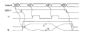
図3は、従来技術に係るSDRAMの動作タイミング図である。 FIG. 3 is an operation timing chart of the SDRAM according to the prior art.
同図を参照すると、アクティブコマンド信号ACTが印加され、ロープリデコード信号RAに対応するメモリセルアレイのワードラインWLがイネーブルされると、セルキャパシタとビットラインBLn、/BLnとの間で電荷共有が行われ、ビットライン対BLn、/BLnの間に微細な電圧差が生じる。 Referring to the figure, when the active command signal ACT is applied and the word line WL of the memory cell array corresponding to the row predecode signal RA is enabled, charge sharing is performed between the cell capacitor and the bit lines BLn and / BLn. As a result, a fine voltage difference is generated between the bit line pair BLn and / BLn.
一方、アクティブコマンド信号ACTの印加時点から一定の遅延時間の後、感知増幅器イネーブル信号SAEN<n>がアクティブになると、RTOライン駆動信号SAPとSBライン駆動信号SANとがアクティブになり、感知増幅器電源ライン駆動部22の2個のNMOSトランジスタがRTOライン及びSBラインをコア電圧VCORE及び接地電圧VSSに駆動する。例えば、メモリセルにデータ「1」が記憶された場合、ビットラインBLnはデータ「1」に対応するコア電圧VCOREレベルに、ビットラインバー/BLnはデータ「0」に対応する接地電圧VSSレベルに増幅する。
On the other hand, when the sense amplifier enable signal SAEN <n> becomes active after a certain delay time from the application time point of the active command signal ACT, the RTO line drive signal SAP and the SB line drive signal SAN become active, and the sense amplifier power supply Two NMOS transistors of the
この後、読み出しコマンド信号RDが印加されると、カラムプリデコード信号CAに対応するカラム選択信号YSがアクティブになり、ビットラインBLn、/BLnに載せられたデータをデータバスを介してコア領域の外部に出力する。
また、書き込みコマンド信号WTが印加されると、同じくカラムプリデコード信号CAに対応するカラム選択信号YSがアクティブになり、データバスに載せられたデータをビットラインBLn、/BLnに書き込む。
Thereafter, when the read command signal RD is applied, the column selection signal YS corresponding to the column predecode signal CA becomes active, and the data loaded on the bit lines BLn and / BLn is transferred to the core area via the data bus. Output to the outside.
When the write command signal WT is applied, the column selection signal YS corresponding to the column predecode signal CA becomes active, and the data loaded on the data bus is written to the bit lines BLn and / BLn.
次いで、ビットラインBLn、/BLnに載せられたデータをメモリセルに書き換える過程を経て、プリチャージコマンド信号PREが印加されると、ワードラインWLを非アクティブにし、感知増幅器イネーブル信号SAEN<n>も非アクティブにすることにより、感知増幅器24をディセーブルさせた後、ビットラインBLn、/BLnをビットラインプリチャージ電圧VBLPレベルにイコライズ及びプリチャージさせる。
Next, when a precharge command signal PRE is applied through a process of rewriting data loaded on the bit lines BLn and / BLn to a memory cell, the word line WL is deactivated and the sense amplifier enable signal SAEN <n> is also set. By deactivating, the
しかし、書き込み動作を行う際、メモリセルに記憶されたデータとは反対のレベルのデータを書き込む場合は、感知増幅器24にラッチされたデータを反転させて駆動しなければならないため、メモリセルに記憶されたデータと同じレベルのデータを書き込む場合に比べて多くの時間を所要し、書き込み回復時間tWRの特性が劣悪になる。
However, when writing data at a level opposite to the data stored in the memory cell during the write operation, the data latched in the
一方、書き込みドライバを拡張して設計すると、書き込み動作速度を改善することができる。しかし、書き込み動作速度の改善のために書き込みドライバを拡張する場合、電流消費が等比級数的に増加してしまう。
そこで、本発明は、上記のような従来技術の問題を解決するためになされたものであり、その目的は、書き込みドライバを拡張させることなく、書き込み動作速度を改善することのできる半導体メモリ素子及びその駆動方法を提供することにある。 Therefore, the present invention has been made to solve the above-described problems of the prior art, and an object of the present invention is to provide a semiconductor memory device capable of improving the write operation speed without expanding the write driver, and The driving method is provided.
上記課題を達成するための本発明の第1の観点によると、ビットライン対に載せられたデータを感知及び増幅するビットライン感知増幅手段と、該ビットライン感知増幅手段の電源ラインを駆動する電源ライン駆動手段と、感知増幅器イネーブル信号に応答して、前記電源ライン駆動手段を制御する駆動制御手段と、アクティブコマンド信号及びプリチャージコマンド信号により定義される期間においてアクティブになり、書き込み動作期間における所定期間に一時的に非アクティブになる前記感知増幅器イネーブル信号を生成する感知増幅器イネーブル信号生成手段とを備える半導体メモリ素子を提供する。 According to a first aspect of the present invention for achieving the above object, there is provided a bit line sense amplification means for sensing and amplifying data placed on a bit line pair, and a power source for driving a power line of the bit line sense amplification means. In response to the sense amplifier enable signal, the line driving means, the drive control means for controlling the power supply line driving means, and the active command signal and the precharge command signal are activated during the period defined by the predetermined period in the write operation period. There is provided a semiconductor memory device comprising sense amplifier enable signal generating means for generating the sense amplifier enable signal that is temporarily inactive during a period.
また、本発明の第2の観点によると、ビットライン対に載せられたデータを感知及び増幅するビットライン感知増幅手段と、該ビットライン感知増幅手段を制御する制御手段とを備え、前記ビットライン感知増幅手段が、書き込み動作期間における所定期間に非アクティブになる半導体メモリ素子を提供する。 According to a second aspect of the present invention, there is provided a bit line sense amplification means for sensing and amplifying data placed on a bit line pair, and a control means for controlling the bit line sense amplification means. A sense amplification means provides a semiconductor memory device that becomes inactive during a predetermined period of a write operation period.
さらに、本発明の第3の観点によると、アクティブコマンド信号及びプリチャージコマンド信号に応答して、第1感知増幅器イネーブル信号を生成するステップと、読み出しコマンド信号及び書き込みコマンド信号に応答して、書き込みカラム選択信号を生成するステップと、前記第1感知増幅器イネーブル信号及び前記書き込みカラム選択信号に応答して、書き込み動作期間における所定期間に一時的に非アクティブになる第2感知増幅器イネーブル信号を生成するステップと、該第2感知増幅器イネーブル信号に応答して、ビットライン対に載せられたデータを感知及び増幅するステップとを含む半導体メモリ素子の駆動方法を提供する。 Further, according to the third aspect of the present invention, a step of generating a first sense amplifier enable signal in response to the active command signal and the precharge command signal, and a writing in response to the read command signal and the write command signal Generating a column selection signal; and, in response to the first sense amplifier enable signal and the write column selection signal, generating a second sense amplifier enable signal that is temporarily inactive during a predetermined period of a write operation period. And a method of driving a semiconductor memory device, the method including sensing and amplifying data placed on the bit line pair in response to the second sense amplifier enable signal.
また、本発明の第4の観点によると、アクティブコマンド信号に応答して、ビットライン感知増幅器をイネーブルさせるステップと、書き込みコマンド信号に応答して、書き込み動作期間における所定期間に一時的に前記ビットライン感知増幅器をディセーブルさせるステップと、前記所定期間の後、再び前記ビットライン感知増幅器をイネーブルさせるステップと、プリチャージコマンド信号に応答して、前記ビットライン感知増幅器をディセーブルさせるステップとを含む半導体メモリ素子の駆動方法を提供する。 According to a fourth aspect of the present invention, the step of enabling a bit line sense amplifier in response to an active command signal and the bit temporarily in a predetermined period of a write operation period in response to a write command signal. Disabling a line sense amplifier; re-enabling the bit line sense amplifier after the predetermined period; and disabling the bit line sense amplifier in response to a precharge command signal. A method for driving a semiconductor memory device is provided.
メモリセルに記憶されたデータとは反対のレベルのデータを書き込む場合、ビットライン感知増幅器のラッチ値を反転させることが、最大のロードとして作用する。本発明では、書き込み動作時、ビットライン感知増幅器を一時的にディセーブルさせて書き込み動作がより速やかに行われるようにした。一方、書き込み動作時、ビットライン感知増幅器のディセーブル期間を定義するために、カラム選択信号を用いることができ、好ましくは、カラム選択信号がアクティブになる直前に、ビットライン感知増幅器がディセーブルされると、電流消費の低減及び書き込み動作時間の短縮の側面において最大の効率を得ることができる。 When writing data at a level opposite to that stored in the memory cell, inverting the latch value of the bit line sense amplifier acts as a maximum load. In the present invention, during the write operation, the bit line sense amplifier is temporarily disabled so that the write operation is performed more quickly. On the other hand, during a write operation, a column select signal can be used to define a disable period of the bit line sense amplifier, preferably the bit line sense amplifier is disabled immediately before the column select signal becomes active. As a result, the maximum efficiency can be obtained in terms of reducing current consumption and shortening the write operation time.
すなわち、第一の発明としては、ビットライン対に載せられたデータを感知及び増幅するビットライン感知増幅手段と、該ビットライン感知増幅手段の電源ラインを駆動する電源ライン駆動手段と、感知増幅器イネーブル信号に応答して、前記電源ライン駆動手段を制御する駆動制御手段と、アクティブコマンド信号及びプリチャージコマンド信号により定義される期間においてアクティブになり、書き込み動作期間における所定期間に一時的に非アクティブになる前記感知増幅器イネーブル信号を生成する感知増幅器イネーブル信号生成手段とを備えることを特徴とする半導体メモリ素子を提供する。 That is, as a first invention, a bit line sense amplification means for sensing and amplifying data placed on a bit line pair, a power line drive means for driving a power line of the bit line sense amplification means, and a sense amplifier enable In response to the signal, it becomes active during a period defined by the drive control means for controlling the power supply line driving means and the active command signal and the precharge command signal, and is temporarily inactive during a predetermined period in the write operation period. And a sense amplifier enable signal generating means for generating the sense amplifier enable signal.
第二の発明としては、ビットライン対に載せられたデータを感知及び増幅するビットライン感知増幅手段と、該ビットライン感知増幅手段を制御する制御手段とを備え、前記ビットライン感知増幅手段が、書き込み動作期間における所定期間に非アクティブになることを特徴とする半導体メモリ素子を提供する。 As a second invention, it comprises a bit line sense amplification means for sensing and amplifying data placed on a bit line pair, and a control means for controlling the bit line sense amplification means, the bit line sense amplification means comprising: Provided is a semiconductor memory device which is inactive during a predetermined period in a write operation period.
第三の発明としては、第二の発明にかかり、アクティブコマンド信号及びプリチャージコマンド信号に応答して、第1感知増幅器イネーブル信号を生成するロー制御手段と、読み出しコマンド信号及び書き込みコマンド信号に応答して、書き込みカラム選択信号を生成するカラム制御手段と、前記第1感知増幅器イネーブル信号及び前記書き込みカラム選択信号に応答して、書き込み動作期間における所定期間に一時的に非アクティブになる第2感知増幅器イネーブル信号を生成する感知増幅器イネーブル制御手段とをさらに備えることを特徴とする半導体メモリ素子を提供する。 As a third invention, according to the second invention, a low control means for generating a first sense amplifier enable signal in response to an active command signal and a precharge command signal, and a response to a read command signal and a write command signal In response to the first sense amplifier enable signal and the write column selection signal, the column control means for generating the write column selection signal and the second sense that becomes temporarily inactive during a predetermined period in the write operation period. A semiconductor memory device is provided, further comprising sense amplifier enable control means for generating an amplifier enable signal.
第四の発明としては、第三の発明にかかり、前記制御手段が、前記ビットライン感知増幅手段の電源ラインを駆動する電源ライン駆動手段と、前記第2感知増幅器イネーブル信号に応答して、前記電源ライン駆動手段を制御する駆動制御手段とを備えることを特徴とする半導体メモリ素子を提供する。 As a fourth invention, according to the third invention, the control means is responsive to a power line driving means for driving a power line of the bit line sense amplification means and the second sense amplifier enable signal, and There is provided a semiconductor memory device comprising drive control means for controlling power supply line drive means.
第五の発明としては、第三の発明にかかり、前記書き込みカラム選択信号が、前記書き込みコマンド信号に対応するカラム選択信号がアクティブになる以前にアクティブになることを特徴とする半導体メモリ素子を提供する。 According to a fifth invention, there is provided the semiconductor memory device according to the third invention, wherein the write column selection signal becomes active before a column selection signal corresponding to the write command signal becomes active. To do.
第六の発明としては、第五の発明にかかり、前記感知増幅器イネーブル制御手段が、前記書き込みカラム選択信号の立ち上がりエッジにおいて所定のパルス幅でアクティブになるパルスを生成するパルス生成部と、該パルス生成部から出力されるパルスと前記第1感知増幅器イネーブル信号との結合を行い、前記第2感知増幅器イネーブル信号を生成する信号結合部とを備えることを特徴とする半導体メモリ素子を提供する。 As a sixth invention, according to the fifth invention, the sense amplifier enable control means generates a pulse that becomes active at a predetermined pulse width at a rising edge of the write column selection signal, and the pulse There is provided a semiconductor memory device comprising: a signal combining unit configured to combine the pulse output from the generation unit and the first sense amplifier enable signal to generate the second sense amplifier enable signal.
第七の発明としては、第六の発明にかかり、前記パルス生成部が、前記書き込みカラム選択信号を遅延させる遅延部と、該遅延部の出力信号を入力とする第1インバータと、前記書き込みカラム選択信号及び前記第1インバータの出力信号を入力とする第1NANDゲートと、該第1NANDゲートの出力信号を入力とする第2インバータと、該第2インバータの出力信号を入力とする第3インバータとを備えることを特徴とする半導体メモリ素子を提供する。 As a seventh invention, according to the sixth invention, the pulse generation unit delays the write column selection signal, a first inverter that receives an output signal of the delay unit, and the write column A first NAND gate that receives the selection signal and the output signal of the first inverter; a second inverter that receives the output signal of the first NAND gate; and a third inverter that receives the output signal of the second inverter; A semiconductor memory device is provided.
第八の発明としては、第七の発明にかかり、前記信号結合部が、前記第3インバータの出力信号及び前記第1感知増幅器イネーブル信号を入力とする第2NANDゲートと、該第2NANDゲートの出力信号を入力とし、前記第2感知増幅器イネーブル信号を出力する第4インバータとを備えることを特徴とする半導体メモリ素子を提供する。 As an eighth invention, according to the seventh invention, the signal coupling unit receives a second NAND gate to which the output signal of the third inverter and the first sense amplifier enable signal are input, and an output of the second NAND gate A semiconductor memory device comprising: a fourth inverter having a signal as an input and outputting the second sense amplifier enable signal.
第九の発明としては、第七の発明にかかり、前記遅延部が、書き込み動作期間において、前記第2感知増幅器イネーブル信号が一時的に非アクティブになる所定期間に該当するだけの遅延時間を有することを特徴とする半導体メモリ素子を提供する。 As a ninth invention, according to the seventh invention, the delay unit has a delay time corresponding to a predetermined period in which the second sense amplifier enable signal is temporarily inactive during the write operation period. A semiconductor memory device is provided.
第十の発明としては、アクティブコマンド信号及びプリチャージコマンド信号に応答して、第1感知増幅器イネーブル信号を生成するステップと、読み出しコマンド信号及び書き込みコマンド信号に応答して、書き込みカラム選択信号を生成するステップと、前記第1感知増幅器イネーブル信号及び前記書き込みカラム選択信号に応答して、書き込み動作期間における所定期間に一時的に非アクティブになる第2感知増幅器イネーブル信号を生成するステップと、該第2感知増幅器イネーブル信号に応答して、ビットライン対に載せられたデータを感知及び増幅するステップとを含むことを特徴とする半導体メモリ素子の駆動方法。 As a tenth aspect of the invention, a step of generating a first sense amplifier enable signal in response to an active command signal and a precharge command signal, and a write column selection signal in response to the read command signal and the write command signal Generating a second sense amplifier enable signal that is temporarily inactive during a predetermined period of a write operation period in response to the first sense amplifier enable signal and the write column selection signal; And sensing and amplifying data placed on the bit line pair in response to a sense amplifier enable signal.
第十一の発明としては、第十の発明にかかり、前記書き込みカラム選択信号が、前記書き込みコマンド信号に対応するカラム選択信号がアクティブになる以前にアクティブになることを特徴とする半導体メモリ素子の駆動方法を提供する。 According to an eleventh aspect of the invention, there is provided the semiconductor memory device according to the tenth aspect, wherein the write column selection signal becomes active before the column selection signal corresponding to the write command signal becomes active. A driving method is provided.
第十二の発明としては、アクティブコマンド信号に応答して、ビットライン感知増幅器をイネーブルさせるステップと、書き込みコマンド信号に応答して、書き込み動作期間における所定期間に一時的に前記ビットライン感知増幅器をディセーブルさせるステップと、前記所定期間の後、再び前記ビットライン感知増幅器をイネーブルさせるステップと、プリチャージコマンド信号に応答して、前記ビットライン感知増幅器をディセーブルさせるステップとを含むことを特徴とする半導体メモリ素子の駆動方法を提供する。 According to a twelfth aspect of the invention, a step of enabling the bit line sense amplifier in response to an active command signal, and a step of temporarily enabling the bit line sense amplifier in a predetermined period in a write operation period in response to a write command signal. Disabling the bit line sense amplifier after the predetermined period, and disabling the bit line sense amplifier in response to a precharge command signal. A method for driving a semiconductor memory device is provided.
第十三の発明としては、第十二の発明にかかり、書き込み動作期間において、前記ビットライン感知増幅器が、書き込みコマンド信号に対応するカラム選択信号がアクティブになる以前にディセーブルされることを特徴とする半導体メモリ素子の駆動方法を提供する。 As a thirteenth invention, according to the twelfth invention, in the write operation period, the bit line sense amplifier is disabled before the column selection signal corresponding to the write command signal becomes active. A method for driving a semiconductor memory device is provided.
以下、添付された図面を参照して本発明の好ましい実施形態をさらに詳細に説明する。 Hereinafter, preferred embodiments of the present invention will be described in detail with reference to the accompanying drawings.
図4は、本発明の一実施形態に係るSDRAMのブロック図である。 FIG. 4 is a block diagram of an SDRAM according to an embodiment of the present invention.
同図を参照すると、本実施形態に係るSDRAMは、外部から入力されるクロックCLK、コマンド/CS、/RAS、/CAS、/WE、アドレス信号A<0:i>をバッファリングし、コマンド/CS、/RAS、/CAS、/WEをデコードして、リフレッシュコマンド信号REF、アクティブコマンド信号ACT、プリチャージコマンド信号PREなどのローコマンド信号と、読み出しコマンド信号RD、書き込みコマンド信号WTのようなカラムコマンド信号を生成する入力バッファ/コマンドデコーダ110と、ローコマンド信号及びアドレス信号A<0:i>に応答して、ロープリデコード信号RA<0:k>と第1感知増幅器イネーブル信号SAENF<0:j>とを生成するロー制御回路120と、カラムコマンド信号及びアドレス信号A<0:i>に応答して、カラムプリデコード信号CA<0:l>と書き込みカラム選択信号YSWとを生成するカラム制御回路130と、第1感知増幅器イネーブル信号SAENF<0:j>及び書き込みカラム選択信号YSWに応答して、第2感知増幅器イネーブル信号SAENS<0:j>を生成する感知増幅器イネーブル信号生成部140とを備える。
Referring to the figure, the SDRAM according to the present embodiment buffers the clock CLK, command / CS, / RAS, / CAS, / WE and address signal A <0: i> input from the outside, CS, / RAS, / CAS, / WE are decoded, and a row command signal such as a refresh command signal REF, an active command signal ACT, and a precharge command signal PRE, and a column such as a read command signal RD and a write command signal WT In response to the input buffer /
また、バンク内には、複数のメモリセルアレイMS0、MS1、…、MSj180と複数のビットライン感知増幅器(BLSA)アレイ190とが交互に配置され、カラムプリデコード信号CA<0:l>を受信して、特定のカラムに対応するカラム選択信号YSをアクティブにするカラムデコーダ160と、ロープリデコード信号RA<0:k>を受信して、ワードラインWL0、WL1、…、WLkを選択するローデコーダ150と、第2感知増幅器イネーブル信号SAENS<0:j>に応答して、ビットライン感知増幅器アレイ190を制御する感知増幅器制御部(SAC)170とを備える。
In the bank, a plurality of memory cell arrays MS0, MS1,..., MSj180 and a plurality of bit line sense amplifier (BLSA)
ビットライン感知増幅器アレイのそれぞれは、その上部及び下部に配置されたメモリセルアレイに共有されるため、それに対応する第2感知増幅器イネーブル信号SAENS<0:j>だけでなく、隣接するビットライン感知増幅器アレイ190に対応する第2感知増幅器イネーブル信号SAENS<0:j>によっても制御される。
Since each of the bit line sense amplifier arrays is shared by the memory cell array disposed above and below the bit line sense amplifier array, not only the corresponding second sense amplifier enable signal SAENS <0: j> but also the adjacent bit line sense amplifiers. It is also controlled by a second sense amplifier enable signal SAENS <0: j> corresponding to the
ここで、書き込みカラム選択信号YSWは、書き込みコマンド信号WTにより生成されるカラム選択信号YSよりも位相の早い信号であって、書き込み動作時、感知増幅器24がディセーブルされる時点を定義する。通常、カラム選択信号YSは、読み出しコマンド信号RD又は書き込みコマンド信号WTのアクティブ時点から一定の遅延時間の後に所定のパルス幅でアクティブになるが、カラム制御回路130でこのカラム選択信号YSの位相を少し早めることにより、書き込みカラム選択信号YSWとして出力するのに困難はない。
Here, the write column selection signal YSW is a signal having a phase earlier than that of the column selection signal YS generated by the write command signal WT, and defines a point in time when the
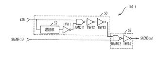
図5は、図4の感知増幅器イネーブル信号生成部140の回路構成を示す図である。感知増幅器イネーブル信号生成部140は、第1感知増幅器イネーブル信号SAENF<0:j>を受信する複数の感知増幅器イネーブル信号生成器を備える。
FIG. 5 is a diagram illustrating a circuit configuration of the sense amplifier enable
感知増幅器イネーブル信号は、それぞれ同じ構造を有するため、そのうち1つを参照すると、感知増幅器イネーブル信号生成器140−1は、書き込みカラム選択信号YSWの立ち上がりエッジにおいて所定のパルス幅でアクティブになるパルスを生成するパルス生成部50と、パルス生成部50から出力されるパルスと第1感知増幅器イネーブル信号SAENF<n>との結合を行い、第2感知増幅器イネーブル信号SAENS<n>を生成する信号結合部55とを備える。
Since each of the sense amplifier enable signals has the same structure, referring to one of them, the sense amplifier enable signal generator 140-1 generates a pulse that becomes active at a predetermined pulse width at the rising edge of the write column selection signal YSW. A
ここで、パルス生成部50は、書き込みカラム選択信号YSWを遅延させる遅延部52と、遅延部52の出力信号を入力とするインバータINV11と、書き込みカラム選択信号YSW及びインバータINV11の出力信号を入力とするNANDゲートNAND11と、NANDゲートNAND11の出力信号を入力とするインバータINV12と、インバータINV12の出力信号を入力とするインバータINV13とを備える。
Here, the
また、信号結合部55は、パルス生成部50の出力信号及び第1感知増幅器イネーブル信号SAENF<n>を入力とするNANDゲートNAND12と、NANDゲートNAND12の出力信号を入力とし、第2感知増幅器イネーブル信号SAENS<n>を出力するインバータINV14とを備える。
The
図6は、図5の遅延部52の回路構成を示す図である。
FIG. 6 is a diagram illustrating a circuit configuration of the
同図を参照すると、遅延部52は、偶数個のインバータで実現されたインバータチェーンと、各インバータの出力端に接続された抵抗と、電源電圧VDDに接続されたPMOSトランジスタ及び接地電圧VSSに接続されたNMOSトランジスタで実現されたキャパシタとを備える。遅延部52の遅延時間は、読み出し動作時、所望の第2感知増幅器イネーブル信号SAENS<n>のディセーブル期間によって設定することができる。
Referring to the figure, the
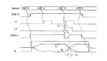
図7は、本発明の一実施形態に係るSDRAMの動作タイミング図である。 FIG. 7 is an operation timing chart of the SDRAM according to the embodiment of the present invention.
同図を参照すると、アクティブコマンド信号ACTが印加され、ロープリデコード信号RAに対応するメモリセルアレイのワードラインWLがイネーブルされると、セルキャパシタとビットラインBLn、/BLnとの間で電荷共有が行われ、ビットライン対BLn、/BLnの間に微細な電圧差が生じる。 Referring to the figure, when the active command signal ACT is applied and the word line WL of the memory cell array corresponding to the row predecode signal RA is enabled, charge sharing is performed between the cell capacitor and the bit lines BLn and / BLn. As a result, a fine voltage difference is generated between the bit line pair BLn and / BLn.
一方、アクティブコマンド信号ACTの印加時点から一定の遅延時間の後、第2感知増幅器イネーブル信号SAENS<n>がアクティブになると、RTOライン駆動信号SAPとSBライン駆動信号SANとがアクティブになり、感知増幅器電源ライン駆動部22の2個のNMOSトランジスタがRTOライン及びSBラインをコア電圧VCORE及び接地電圧VSSによって駆動させる。
On the other hand, when the second sense amplifier enable signal SAENS <n> becomes active after a certain delay time from the application time point of the active command signal ACT, the RTO line drive signal SAP and the SB line drive signal SAN become active and sense. Two NMOS transistors of the amplifier
この後、読み出しコマンド信号RDが印加されると、カラムプリデコード信号CAに対応するカラム選択信号YSがアクティブになり、ビットラインBLn、/BLnに載せられたデータをデータバスを介してコア領域の外部に出力する。このとき、書き込みカラム選択信号YSWは、書き込みコマンド信号WTの印加時にのみアクティブになる信号であるため、読み出し動作時には非アクティブになり、このときの動作は従来技術と同様である。 Thereafter, when the read command signal RD is applied, the column selection signal YS corresponding to the column predecode signal CA becomes active, and the data loaded on the bit lines BLn and / BLn is transferred to the core area via the data bus. Output to the outside. At this time, the write column selection signal YSW is a signal that becomes active only when the write command signal WT is applied, so that it becomes inactive during the read operation, and the operation at this time is the same as in the prior art.
また、書き込みコマンド信号WTが印加されると、同じくカラムプリデコード信号CAに対応するカラム選択信号YSがアクティブになり、データバスに載せられたデータをビットラインBLn、/BLnに書き込む。このとき、書き込みカラム選択信号YSWがカラム選択信号YSよりも時間の量D3だけ先にアクティブになり、書き込みカラム選択信号YSWのアクティブ時点から感知増幅器イネーブル制御部140の遅延部52の時間の量D1に対応する期間に第2感知増幅器イネーブル信号SAENS<n>が非アクティブになる。
When the write command signal WT is applied, the column selection signal YS corresponding to the column predecode signal CA becomes active, and the data loaded on the data bus is written to the bit lines BLn and / BLn. At this time, the write column selection signal YSW becomes active earlier than the column selection signal YS by an amount of time D3, and the amount of time D1 of the
この後、第2感知増幅器イネーブル信号SAENS<n>が再びアクティブになり、ビットラインBLn、/BLnに載せられたデータをメモリセルに書き換える過程を経て、プリチャージコマンド信号PREが印加されると、ワードラインWLは非アクティブになり、第2感知増幅器イネーブル信号SAENS<n>も同じく非アクティブになることにより、感知増幅器24をディセーブルさせた後、ビットラインBLn、/BLnをビットラインプリチャージ電圧VBLPレベルにイコライズ及びプリチャージさせる。
以上、本実施形態によると、書き込み動作時、感知増幅器24が一時的にディセーブルされた状態で書き込みドライバがデータをビットラインBLn、/BLnに駆動するため、メモリセルに記憶されたデータとは反対のレベルのデータを書き込む場合、従来に比べて時間の量D2だけ先に感知増幅器24にラッチされたデータを反転させることができる。したがって、それだけ書き込み動作速度が速くなる。これは、書き込み回復時間tWRの特性が改善されることを意味する。
Thereafter, the second sense amplifier enable signal SAENS <n> becomes active again, and when the precharge command signal PRE is applied through a process of rewriting data loaded on the bit lines BLn and / BLn into memory cells, The word line WL becomes inactive, and the second sense amplifier enable signal SAENS <n> is also inactive, thereby disabling the
As described above, according to the present embodiment, during the write operation, the write driver drives the data to the bit lines BLn and / BLn while the
前述の実施形態では、書き込みカラム選択信号として書き込みコマンド信号WTにより生成されるカラム選択信号YSよりも位相の早い書き込みカラム選択信号YSWを用いて、書き込み動作時、一時的に感知増幅器をディセーブルさせる場合を一例として説明したが、場合によっては、書き込みコマンド信号WTにより生成されるカラム選択信号YSを書き込みカラム選択信号として直接用いたり、それよりも位相の遅い信号を用いることができる。この場合、本実施形態に比べて、動作時間の側面において効率はやや落ちるが、従来技術に比べて有利であることは間違いない。 In the above-described embodiment, the sense amplifier is temporarily disabled during the write operation by using the write column selection signal YSW having a phase earlier than the column selection signal YS generated by the write command signal WT as the write column selection signal. Although the case has been described as an example, in some cases, the column selection signal YS generated by the write command signal WT can be directly used as the write column selection signal, or a signal with a phase later than that can be used. In this case, the efficiency is slightly reduced in terms of operation time compared to the present embodiment, but there is no doubt that it is advantageous over the prior art.
また、前述の実施形態では、ノーマルドライブ構造を適用する場合を一例として説明したが、本発明は、オーバードライブ構造を適用する場合にも適用される。 In the above-described embodiment, the case where the normal drive structure is applied has been described as an example. However, the present invention is also applied to the case where the overdrive structure is applied.
なお、前述の実施形態において、感知増幅器イネーブル信号生成部の回路構成を示す例は、可能な数多くの実現例の一部に過ぎず、用いられる信号の種類及びそのアクティブ極性によってその他の構成への変更が欠かせない。 In the above-described embodiment, the example of the circuit configuration of the sense amplifier enable signal generation unit is only a part of many possible implementation examples. Depending on the type of signal used and its active polarity, other configurations can be used. Change is essential.
さらに、前述の実施形態では、SDRAMを一例として説明したが、本発明は、ノーマルDRAM、DDR、DDR2、DDR3のような、ビットライン感知増幅器を備える全ての半導体メモリ素子に適用することができる。 Furthermore, in the above-described embodiments, the SDRAM has been described as an example. However, the present invention can be applied to all semiconductor memory devices including a bit line sense amplifier such as a normal DRAM, DDR, DDR2, and DDR3.
本発明は、書き込み動作時間を短縮し、書き込み回復時間tWRの特性を改善するという効果がある。一方、本発明を適用すると、書き込みドライバを拡張して設計する必要がないため、電流消費の増加を抑制することができる。 The present invention has an effect of shortening the write operation time and improving the characteristics of the write recovery time tWR. On the other hand, when the present invention is applied, it is not necessary to expand and design the write driver, so that increase in current consumption can be suppressed.
以上、本発明は、上記した実施形態に限定されるものではなく、本発明に係る技術的思想の範囲から逸脱しない範囲内で様々な変更が可能であり、それらも本発明の技術的範囲に属する。 As described above, the present invention is not limited to the above-described embodiment, and various modifications can be made without departing from the scope of the technical idea according to the present invention, and these are also within the technical scope of the present invention. Belongs.
110 入力バッファ/コマンドデコーダ
120 ロー制御部
130 カラム制御部
140 感知増幅器イネーブル信号生成部
150 ローデコーダ
160 カラムデコーダ
170 感知増幅器制御部(SAC)
180 メモリセルアレイ
190 ビットライン感知増幅器(BLSA)アレイ
110 Input Buffer /
180
Claims (13)
該ビットライン感知増幅手段の電源ラインを駆動する電源ライン駆動手段と、
感知増幅器イネーブル信号に応答して、前記電源ライン駆動手段を制御する駆動制御手段と、
アクティブコマンド信号及びプリチャージコマンド信号により定義される期間においてアクティブになり、書き込み動作期間における所定期間に一時的に非アクティブになる前記感知増幅器イネーブル信号を生成する感知増幅器イネーブル信号生成手段と
を備えることを特徴とする半導体メモリ素子。 Bit line sense amplification means for sensing and amplifying data placed on the bit line pair;
Power line driving means for driving the power line of the bit line sense amplification means;
Drive control means for controlling the power line drive means in response to a sense amplifier enable signal;
Sense amplifier enable signal generating means for generating the sense amplifier enable signal that is active in a period defined by an active command signal and a precharge command signal and temporarily inactive in a predetermined period in a write operation period. A semiconductor memory device.
該ビットライン感知増幅手段を制御する制御手段と
を備え、
前記ビットライン感知増幅手段が、書き込み動作期間における所定期間に非アクティブになることを特徴とする半導体メモリ素子。 Bit line sense amplification means for sensing and amplifying data placed on the bit line pair;
Control means for controlling the bit line sense amplification means,
The semiconductor memory device, wherein the bit line sense amplification means is inactive during a predetermined period of a write operation period.
読み出しコマンド信号及び書き込みコマンド信号に応答して、書き込みカラム選択信号を生成するカラム制御手段と、
前記第1感知増幅器イネーブル信号及び前記書き込みカラム選択信号に応答して、書き込み動作期間における所定期間に一時的に非アクティブになる第2感知増幅器イネーブル信号を生成する感知増幅器イネーブル制御手段と
をさらに備えることを特徴とする請求項2に記載の半導体メモリ素子。 Low control means for generating a first sense amplifier enable signal in response to the active command signal and the precharge command signal;
Column control means for generating a write column selection signal in response to the read command signal and the write command signal;
Sense amplifier enable control means for generating a second sense amplifier enable signal that is temporarily inactive during a predetermined period of a write operation period in response to the first sense amplifier enable signal and the write column selection signal. The semiconductor memory device according to claim 2.
前記ビットライン感知増幅手段の電源ラインを駆動する電源ライン駆動手段と、
前記第2感知増幅器イネーブル信号に応答して、前記電源ライン駆動手段を制御する駆動制御手段と
を備えることを特徴とする請求項3に記載の半導体メモリ素子。 The control means is
Power line driving means for driving the power line of the bit line sense amplification means;
4. The semiconductor memory device of claim 3, further comprising drive control means for controlling the power line drive means in response to the second sense amplifier enable signal.
前記書き込みカラム選択信号の立ち上がりエッジにおいて所定のパルス幅でアクティブになるパルスを生成するパルス生成部と、
該パルス生成部から出力されるパルスと前記第1感知増幅器イネーブル信号との結合を行い、前記第2感知増幅器イネーブル信号を生成する信号結合部と
を備えることを特徴とする請求項5に記載の半導体メモリ素子。 The sense amplifier enable control means;
A pulse generator for generating a pulse that becomes active at a predetermined pulse width at a rising edge of the write column selection signal;
6. The signal combining unit according to claim 5, further comprising a signal combining unit configured to combine the pulse output from the pulse generation unit with the first sense amplifier enable signal and generate the second sense amplifier enable signal. Semiconductor memory device.
前記書き込みカラム選択信号を遅延させる遅延部と、
該遅延部の出力信号を入力とする第1インバータと、
前記書き込みカラム選択信号及び前記第1インバータの出力信号を入力とする第1NANDゲートと、
該第1NANDゲートの出力信号を入力とする第2インバータと、
該第2インバータの出力信号を入力とする第3インバータと
を備えることを特徴とする請求項6に記載の半導体メモリ素子。 The pulse generator is
A delay unit for delaying the write column selection signal;
A first inverter that receives the output signal of the delay unit;
A first NAND gate having the write column selection signal and the output signal of the first inverter as inputs;
A second inverter that receives the output signal of the first NAND gate;
The semiconductor memory device according to claim 6, further comprising a third inverter that receives an output signal of the second inverter.
前記第3インバータの出力信号及び前記第1感知増幅器イネーブル信号を入力とする第2NANDゲートと、
該第2NANDゲートの出力信号を入力とし、前記第2感知増幅器イネーブル信号を出力する第4インバータと
を備えることを特徴とする請求項7に記載の半導体メモリ素子。 The signal coupling unit is
A second NAND gate receiving the output signal of the third inverter and the first sense amplifier enable signal;
The semiconductor memory device of claim 7, further comprising a fourth inverter that receives an output signal of the second NAND gate and outputs the second sense amplifier enable signal.
読み出しコマンド信号及び書き込みコマンド信号に応答して、書き込みカラム選択信号を生成するステップと、
前記第1感知増幅器イネーブル信号及び前記書き込みカラム選択信号に応答して、書き込み動作期間における所定期間に一時的に非アクティブになる第2感知増幅器イネーブル信号を生成するステップと、
該第2感知増幅器イネーブル信号に応答して、ビットライン対に載せられたデータを感知及び増幅するステップと
を含むことを特徴とする半導体メモリ素子の駆動方法。 Generating a first sense amplifier enable signal in response to the active command signal and the precharge command signal;
Generating a write column selection signal in response to the read command signal and the write command signal;
Generating a second sense amplifier enable signal that is temporarily inactive during a predetermined period of a write operation period in response to the first sense amplifier enable signal and the write column selection signal;
A method of driving a semiconductor memory device, comprising: sensing and amplifying data placed on a bit line pair in response to the second sense amplifier enable signal.
書き込みコマンド信号に応答して、書き込み動作期間における所定期間に一時的に前記ビットライン感知増幅器をディセーブルさせるステップと、
前記所定期間の後、再び前記ビットライン感知増幅器をイネーブルさせるステップと、
プリチャージコマンド信号に応答して、前記ビットライン感知増幅器をディセーブルさせるステップと
を含むことを特徴とする半導体メモリ素子の駆動方法。 Enabling a bit line sense amplifier in response to an active command signal;
In response to a write command signal, temporarily disabling the bit line sense amplifier during a predetermined period of a write operation period;
Enabling the bitline sense amplifier again after the predetermined period;
Disabling the bitline sense amplifier in response to a precharge command signal.
Applications Claiming Priority (1)
| Application Number | Priority Date | Filing Date | Title |
|---|---|---|---|
| KR1020060060892A KR100780613B1 (en) | 2006-06-30 | 2006-06-30 | Semiconductor memory device and driving method thereof |
Publications (1)
| Publication Number | Publication Date |
|---|---|
| JP2008016169A true JP2008016169A (en) | 2008-01-24 |
Family
ID=38876471
Family Applications (1)
| Application Number | Title | Priority Date | Filing Date |
|---|---|---|---|
| JP2007050765A Pending JP2008016169A (en) | 2006-06-30 | 2007-02-28 | Semiconductor memory device and driving method thereof |
Country Status (3)
| Country | Link |
|---|---|
| US (1) | US7599238B2 (en) |
| JP (1) | JP2008016169A (en) |
| KR (1) | KR100780613B1 (en) |
Cited By (1)
| Publication number | Priority date | Publication date | Assignee | Title |
|---|---|---|---|---|
| JP2011175696A (en) * | 2010-02-23 | 2011-09-08 | Elpida Memory Inc | Semiconductor device |
Families Citing this family (10)
| Publication number | Priority date | Publication date | Assignee | Title |
|---|---|---|---|---|
| KR100949277B1 (en) * | 2008-08-20 | 2010-03-25 | 주식회사 하이닉스반도체 | Data Input Buffer Enable Signal Generation Circuit and Method |
| KR101115453B1 (en) | 2010-02-26 | 2012-02-24 | 주식회사 하이닉스반도체 | Semiconductor memory device and operating method for the same |
| KR101171254B1 (en) | 2010-05-31 | 2012-08-06 | 에스케이하이닉스 주식회사 | Control Circuit for Bit-line Sense Amplifier and Semiconductor Memory Apparatus Having the Same |
| KR101223537B1 (en) | 2010-10-29 | 2013-01-21 | 에스케이하이닉스 주식회사 | Semiconductor Memory Apparatus |
| KR20120120759A (en) * | 2011-04-25 | 2012-11-02 | 에스케이하이닉스 주식회사 | Semiconductor integrated circuit and method of driving the same |
| JP2012230737A (en) * | 2011-04-26 | 2012-11-22 | Elpida Memory Inc | Semiconductor device |
| KR101895420B1 (en) * | 2012-05-25 | 2018-09-06 | 에스케이하이닉스 주식회사 | Sense Amplifier Control Circuit And Semiconductor Memory Apparatus Including The Same |
| KR101654725B1 (en) * | 2015-01-16 | 2016-09-06 | 엘지전자 주식회사 | cooking appliance |
| US9978444B2 (en) * | 2016-03-22 | 2018-05-22 | Qualcomm Incorporated | Sense amplifier enabling scheme |
| KR102773416B1 (en) | 2019-07-05 | 2025-02-28 | 삼성전자주식회사 | Semiconductor memory device and data write method thereof |
Citations (6)
| Publication number | Priority date | Publication date | Assignee | Title |
|---|---|---|---|---|
| JPH03165398A (en) * | 1989-11-24 | 1991-07-17 | Matsushita Electric Ind Co Ltd | RAM readout circuit |
| JPH0785669A (en) * | 1993-09-17 | 1995-03-31 | Fujitsu Ltd | Semiconductor memory device |
| JPH08335392A (en) * | 1995-06-08 | 1996-12-17 | Miyagi Oki Denki Kk | Sense amplifier circuit for semiconductor memory |
| JPH11126481A (en) * | 1997-10-20 | 1999-05-11 | Fujitsu Ltd | Semiconductor storage device |
| JPH11339474A (en) * | 1998-05-22 | 1999-12-10 | Matsushita Electric Ind Co Ltd | Semiconductor storage device |
| JP2003196983A (en) | 2001-12-27 | 2003-07-11 | Mitsubishi Electric Corp | Semiconductor storage device |
Family Cites Families (11)
| Publication number | Priority date | Publication date | Assignee | Title |
|---|---|---|---|---|
| US4678618A (en) | 1984-08-20 | 1987-07-07 | Westinghouse Electric Corp. | Individual source positioning mechanism for a nuclear reactor fuel assembly |
| JPH04278288A (en) * | 1991-03-07 | 1992-10-02 | Toshiba Corp | Semiconductor storage device |
| JPH0536277A (en) | 1991-07-30 | 1993-02-12 | Fujitsu Ltd | Semiconductor memory device |
| US5982692A (en) | 1997-08-01 | 1999-11-09 | International Business Machines Corporation | Bit line boost amplifier |
| KR100295048B1 (en) * | 1998-07-23 | 2001-07-12 | 윤종용 | Memory device for minimizing write time and method for writing data using the same |
| KR100373350B1 (en) * | 1999-04-19 | 2003-02-25 | 주식회사 하이닉스반도체 | Low power embedded sram |
| JP2001101863A (en) * | 1999-09-27 | 2001-04-13 | Fujitsu Ltd | Semiconductor integrated circuit and control method thereof |
| KR100394066B1 (en) * | 2000-09-29 | 2003-08-09 | 주식회사 하이닉스반도체 | Data write circuit for semiconductor memory |
| JP2004199842A (en) * | 2002-12-20 | 2004-07-15 | Nec Micro Systems Ltd | Semiconductor memory and method for controlling the same |
| JP2004213830A (en) * | 2003-01-08 | 2004-07-29 | Sony Corp | Semiconductor storage device |
| KR20190000930U (en) * | 2017-10-12 | 2019-04-22 | 두리기농업회사법인 주식회사 | roaster of tea |
-
2006
- 2006-06-30 KR KR1020060060892A patent/KR100780613B1/en not_active Expired - Fee Related
- 2006-12-29 US US11/647,318 patent/US7599238B2/en active Active
-
2007
- 2007-02-28 JP JP2007050765A patent/JP2008016169A/en active Pending
Patent Citations (6)
| Publication number | Priority date | Publication date | Assignee | Title |
|---|---|---|---|---|
| JPH03165398A (en) * | 1989-11-24 | 1991-07-17 | Matsushita Electric Ind Co Ltd | RAM readout circuit |
| JPH0785669A (en) * | 1993-09-17 | 1995-03-31 | Fujitsu Ltd | Semiconductor memory device |
| JPH08335392A (en) * | 1995-06-08 | 1996-12-17 | Miyagi Oki Denki Kk | Sense amplifier circuit for semiconductor memory |
| JPH11126481A (en) * | 1997-10-20 | 1999-05-11 | Fujitsu Ltd | Semiconductor storage device |
| JPH11339474A (en) * | 1998-05-22 | 1999-12-10 | Matsushita Electric Ind Co Ltd | Semiconductor storage device |
| JP2003196983A (en) | 2001-12-27 | 2003-07-11 | Mitsubishi Electric Corp | Semiconductor storage device |
Cited By (1)
| Publication number | Priority date | Publication date | Assignee | Title |
|---|---|---|---|---|
| JP2011175696A (en) * | 2010-02-23 | 2011-09-08 | Elpida Memory Inc | Semiconductor device |
Also Published As
| Publication number | Publication date |
|---|---|
| KR100780613B1 (en) | 2007-11-29 |
| US20080002498A1 (en) | 2008-01-03 |
| US7599238B2 (en) | 2009-10-06 |
Similar Documents
| Publication | Publication Date | Title |
|---|---|---|
| JP2008016169A (en) | Semiconductor memory device and driving method thereof | |
| JP5595236B2 (en) | Semiconductor device | |
| KR100757926B1 (en) | Sense Amplifier Control Circuit and Method of Semiconductor Memory Device | |
| US10504582B2 (en) | Timing control circuit shared by a plurality of banks | |
| US20160307618A1 (en) | Sense amplifier and semiconductor device for securing operation margin of sense amplifier | |
| KR20100071153A (en) | Semiconductor memory device having improved precharge scheme for local i/o lines | |
| KR20040038449A (en) | Semiconductor memory device having hierachical data input/output line and method for precharging therefor | |
| KR20100102817A (en) | Control signal driving circuit in semiconductor device | |
| JP2007012244A (en) | Latency control circuit for semiconductor memory device | |
| JP4629249B2 (en) | Semiconductor memory device and information reading method thereof | |
| US6542426B2 (en) | Cell data protection circuit in semiconductor memory device and method of driving refresh mode | |
| US20070268764A1 (en) | Low voltage sense amplifier and sensing method | |
| KR100695524B1 (en) | Semiconductor memory device and driving method thereof | |
| KR100625793B1 (en) | Semiconductor memory device | |
| KR100847315B1 (en) | Self refresh control circuit, semiconductor memory device and self refresh control method including the same | |
| JP4982686B2 (en) | Circuit for generating overdriver control signal of semiconductor memory device | |
| US8159860B2 (en) | Semiconductor memory device having a discharge path generator for global I/O lines | |
| KR20110025487A (en) | Semiconductor memory device | |
| US20110069573A1 (en) | Semiconductor memory device | |
| US8194485B2 (en) | Semiconductor memory device and method of controlling sense amplifier of semiconductor memory device | |
| US20080080273A1 (en) | Over-drive control signal generator for use in semiconductor memory device | |
| KR100838364B1 (en) | Amplification Enable Signal Generation Circuit of Semiconductor Memory Device | |
| US12537044B2 (en) | Semiconductor device and memory device including complementary delay circuits for maximizing operation efficiency while minimizing area occupied by delay circuits | |
| KR101020285B1 (en) | Word line signal generation circuit | |
| KR20140060684A (en) | Circuit for generating overdrive pulse and column selecting pulse of a semiconductor memory apparatus |
Legal Events
| Date | Code | Title | Description |
|---|---|---|---|
| A621 | Written request for application examination |
Free format text: JAPANESE INTERMEDIATE CODE: A621 Effective date: 20100218 |
|
| A521 | Written amendment |
Free format text: JAPANESE INTERMEDIATE CODE: A523 Effective date: 20110316 |
|
| A131 | Notification of reasons for refusal |
Free format text: JAPANESE INTERMEDIATE CODE: A131 Effective date: 20111115 |
|
| A521 | Written amendment |
Free format text: JAPANESE INTERMEDIATE CODE: A523 Effective date: 20120214 |
|
| RD02 | Notification of acceptance of power of attorney |
Free format text: JAPANESE INTERMEDIATE CODE: A7422 Effective date: 20120322 |
|
| RD04 | Notification of resignation of power of attorney |
Free format text: JAPANESE INTERMEDIATE CODE: A7424 Effective date: 20120402 |
|
| A02 | Decision of refusal |
Free format text: JAPANESE INTERMEDIATE CODE: A02 Effective date: 20120828 |
|
| A521 | Written amendment |
Free format text: JAPANESE INTERMEDIATE CODE: A523 Effective date: 20121226 |
|
| A911 | Transfer to examiner for re-examination before appeal (zenchi) |
Free format text: JAPANESE INTERMEDIATE CODE: A911 Effective date: 20130213 |
|
| A912 | Re-examination (zenchi) completed and case transferred to appeal board |
Free format text: JAPANESE INTERMEDIATE CODE: A912 Effective date: 20130510 |