JP2008022011A - プリント配線板のための圧着装置 - Google Patents
プリント配線板のための圧着装置 Download PDFInfo
- Publication number
- JP2008022011A JP2008022011A JP2007183560A JP2007183560A JP2008022011A JP 2008022011 A JP2008022011 A JP 2008022011A JP 2007183560 A JP2007183560 A JP 2007183560A JP 2007183560 A JP2007183560 A JP 2007183560A JP 2008022011 A JP2008022011 A JP 2008022011A
- Authority
- JP
- Japan
- Prior art keywords
- printed wiring
- wiring board
- spring element
- crimping device
- guide
- Prior art date
- Legal status (The legal status is an assumption and is not a legal conclusion. Google has not performed a legal analysis and makes no representation as to the accuracy of the status listed.)
- Granted
Links
- 238000002788 crimping Methods 0.000 title claims description 12
- 238000003780 insertion Methods 0.000 claims abstract description 38
- 230000037431 insertion Effects 0.000 claims abstract description 38
- 239000004020 conductor Substances 0.000 claims description 6
- 238000004519 manufacturing process Methods 0.000 description 5
- 239000000463 material Substances 0.000 description 2
- 238000000034 method Methods 0.000 description 2
- 238000003825 pressing Methods 0.000 description 2
- 239000002184 metal Substances 0.000 description 1
- 239000007769 metal material Substances 0.000 description 1
Images
Classifications
-
- H—ELECTRICITY
- H05—ELECTRIC TECHNIQUES NOT OTHERWISE PROVIDED FOR
- H05K—PRINTED CIRCUITS; CASINGS OR CONSTRUCTIONAL DETAILS OF ELECTRIC APPARATUS; MANUFACTURE OF ASSEMBLAGES OF ELECTRICAL COMPONENTS
- H05K7/00—Constructional details common to different types of electric apparatus
- H05K7/14—Mounting supporting structure in casing or on frame or rack
- H05K7/1417—Mounting supporting structure in casing or on frame or rack having securing means for mounting boards, plates or wiring boards
- H05K7/1418—Card guides, e.g. grooves
Landscapes
- Engineering & Computer Science (AREA)
- Microelectronics & Electronic Packaging (AREA)
- Coupling Device And Connection With Printed Circuit (AREA)
- Mounting Of Printed Circuit Boards And The Like (AREA)
Abstract
【解決手段】プリント配線板差込みケーシング内にて上側及び下側の案内レール10,14の間に押込み可能なプリント配線板1を圧着する圧着装置であって、前記案内レール10,14の一方内に前記プリント配線板1の狭幅側2の上に作用するばねエレメントを設ける。
【選択図】図1
Description
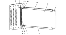
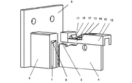
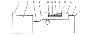
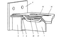
3 段部
4 縁部
5 バックプレーン
6 カードエッジ差込み
7 差込みスリット
10 案内レール
11 切欠き
12 側脚部
13 ステー
14 案内レール
16 ばねエレメント
17 ばねアーム
18 円弧部
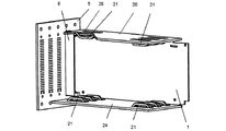
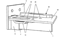
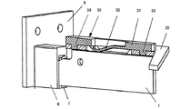
20 天板
21 案内ステー
22 切欠き
24 底板
25 孔
26 ばねエレメント
30 ばねエレメント
31 係止ピン
32 ばねアーム
33 プラスチック体
Claims (7)
- プリント配線板の上に設けられた導体路を、カードエッジ差込みコネクタ(6)内に配置された対応する電気的な接点に正確に接触させるために、プリント配線板差込みケーシング内にて上側及び下側の案内レール(10,14)の間に押込み可能なプリント配線板(1)を圧着する圧着装置であって、前記案内レール(10,14)の一方(10)内に前記プリント配線板(1)の狭幅側(2)の上に作用するばねエレメント(16,26,30)が設けられていることを特徴とする、プリント配線板のための圧着装置。
- 前記案内レールが別個に取付け可能な案内レール(10,14)として構成されており、一方の案内レール(10)にスライド方向に配向されたばねエレメント(16)が配置されている、請求項1記載の圧着装置。
- 前記案内レール(10,14)が案内ステー(21)として構成され、前記プリント配線板(1)を取囲むプリント配線板ケーシングの天板(20)と底板(24)にてプリント配線板(1)の両側に構成され、この場合、上側の案内ステー(21)の内部でばねエレメント(26)が一体成形されたエレメントとして前記プリント配線板のスライド方向に配置されている、請求項1記載の圧着装置。
- 前記天板(20)に設けられた案内ステー(21)内に別個に挿入可能なばねエレメント(30)が配置されている、請求項3記載の圧着装置。
- 前記ばねエレメント(16)が常に片側で、プリント配線板(1)の狭幅側に作用するように、差込まれたプリント配線板(1)の段部(3)の近くに配置されている、請求項1から4までのいずれか1項記載の圧着装置。
- 前記カードエッジ差込みコネクタ(6)がそれぞれ下側の案内レールで前記プリント配線の下側の段部(3′)と前記差込みスリット(7)の下側の縁(8′)との間の最小の高さ許容誤差に調節されている、請求項1から5までのいずれか1項記載の圧着装置。
- 前記カードエッジ差込みコネクタ(6)の差込みスリット(7)の下側の縁(8′)が前記プリント配線板(1)の段部(3′)に対し高められた位置を有している、請求項1から6までのいずれか1項記載の圧着装置。
Applications Claiming Priority (1)
| Application Number | Priority Date | Filing Date | Title |
|---|---|---|---|
| DE202006010806U DE202006010806U1 (de) | 2006-07-13 | 2006-07-13 | Andruckvorrichtung für eine Leiterplatte |
Publications (2)
| Publication Number | Publication Date |
|---|---|
| JP2008022011A true JP2008022011A (ja) | 2008-01-31 |
| JP4427569B2 JP4427569B2 (ja) | 2010-03-10 |
Family
ID=37111990
Family Applications (1)
| Application Number | Title | Priority Date | Filing Date |
|---|---|---|---|
| JP2007183560A Expired - Fee Related JP4427569B2 (ja) | 2006-07-13 | 2007-07-12 | プリント配線板のための圧着装置 |
Country Status (6)
| Country | Link |
|---|---|
| US (1) | US8077471B2 (ja) |
| EP (1) | EP1879441B1 (ja) |
| JP (1) | JP4427569B2 (ja) |
| CN (1) | CN101106882B (ja) |
| CA (1) | CA2593216C (ja) |
| DE (1) | DE202006010806U1 (ja) |
Cited By (1)
| Publication number | Priority date | Publication date | Assignee | Title |
|---|---|---|---|---|
| JP2011222908A (ja) * | 2010-04-14 | 2011-11-04 | Fujitsu Telecom Networks Ltd | プラグインパッケージをスライド収納するシェルフと電子装置 |
Families Citing this family (3)
| Publication number | Priority date | Publication date | Assignee | Title |
|---|---|---|---|---|
| GB2562737B (en) | 2017-05-23 | 2020-06-10 | Ge Aviat Systems Ltd | Power management panel and controller assembly |
| US11455019B2 (en) * | 2020-08-19 | 2022-09-27 | Quanta Computer Inc. | Docking system having elastic rail portions |
| DE102022117747A1 (de) * | 2022-07-15 | 2024-01-18 | Connaught Electronics Ltd. | Steuerungsvorrichtungsanordnung für ein Fahrzeug und Verfahren zum Montieren einer Steuerungsvorrichtungsanordnung |
Family Cites Families (14)
| Publication number | Priority date | Publication date | Assignee | Title |
|---|---|---|---|---|
| US34190A (en) * | 1862-01-21 | Improved rotary engine | ||
| JPS4844453A (ja) | 1971-10-11 | 1973-06-26 | ||
| US3899721A (en) * | 1974-03-20 | 1975-08-12 | Bell Telephone Labor Inc | Printed circuit card guide |
| US4609987A (en) | 1983-03-09 | 1986-09-02 | Safe Flight Instrument Corporation | Aircraft guidance system for take off or go-around during severe wind shear |
| US4619490A (en) | 1984-12-18 | 1986-10-28 | Raychem Corporation | Guidance and retention device and connector assembly |
| SE501896C2 (sv) * | 1993-10-12 | 1995-06-12 | Ellemtel Utvecklings Ab | Elektriskt anslutningsarrangemang |
| US5392629A (en) * | 1993-10-26 | 1995-02-28 | Canoga Industries Inc. | Method and apparatus for forming multi-level features in an object |
| US5467254A (en) | 1993-11-04 | 1995-11-14 | Synoptics Communications, Inc. | Supportive guide for circuit-card grounding including tracks having staggered protrusions at the proximal end of the tracks |
| JPH10509835A (ja) * | 1994-11-30 | 1998-09-22 | ミネソタ・マイニング・アンド・マニュファクチュアリング・カンパニー | 多層積層構造の電気コネクタアセンブリ及び製造方法 |
| US5617296A (en) * | 1995-05-17 | 1997-04-01 | International Business Machines Corporation | Printed circuit board covers for an electronics package |
| GB9815339D0 (en) * | 1998-07-16 | 1998-09-16 | British Aerospace | Wedgelock installation device |
| DE19833248C2 (de) * | 1998-07-23 | 2002-09-19 | Rohde & Schwarz | Vorrichtung zum Führen und Massekontaktieren von Leiterplatten |
| DE29912419U1 (de) | 1999-07-15 | 1999-10-28 | Chien, Yung-Chih, Pa-Li Hsiang, Taipeh | Schnappbefestigungseinrichtung für Computerschnittstellenkarte |
| TW549689U (en) * | 2002-11-13 | 2003-08-21 | Tekcon Electronics Corp | Electrical card connector |
-
2006
- 2006-07-13 DE DE202006010806U patent/DE202006010806U1/de not_active Expired - Lifetime
-
2007
- 2007-06-27 US US11/769,577 patent/US8077471B2/en not_active Expired - Fee Related
- 2007-07-03 EP EP07012970.5A patent/EP1879441B1/de not_active Not-in-force
- 2007-07-06 CA CA2593216A patent/CA2593216C/en not_active Expired - Fee Related
- 2007-07-12 JP JP2007183560A patent/JP4427569B2/ja not_active Expired - Fee Related
- 2007-07-13 CN CN2007101291381A patent/CN101106882B/zh not_active Expired - Fee Related
Cited By (1)
| Publication number | Priority date | Publication date | Assignee | Title |
|---|---|---|---|---|
| JP2011222908A (ja) * | 2010-04-14 | 2011-11-04 | Fujitsu Telecom Networks Ltd | プラグインパッケージをスライド収納するシェルフと電子装置 |
Also Published As
| Publication number | Publication date |
|---|---|
| EP1879441B1 (de) | 2016-08-17 |
| CA2593216C (en) | 2010-06-01 |
| CN101106882A (zh) | 2008-01-16 |
| US20080013261A1 (en) | 2008-01-17 |
| CN101106882B (zh) | 2010-10-13 |
| EP1879441A3 (de) | 2014-04-23 |
| DE202006010806U1 (de) | 2006-10-05 |
| CA2593216A1 (en) | 2008-01-13 |
| EP1879441A2 (de) | 2008-01-16 |
| JP4427569B2 (ja) | 2010-03-10 |
| US8077471B2 (en) | 2011-12-13 |
Similar Documents
| Publication | Publication Date | Title |
|---|---|---|
| US7497697B2 (en) | PCB connector including plug and socket contacts for easy positioning | |
| JP5197294B2 (ja) | 基板対基板コネクタ | |
| US7780476B2 (en) | Electrical card connector | |
| JP5141923B2 (ja) | コネクタ装置 | |
| JP2010097724A (ja) | 基板対基板コネクタ | |
| US6808412B2 (en) | Cable connector | |
| JP2007227379A (ja) | プリント配線板差込延長部 | |
| KR101326395B1 (ko) | 커넥터 및 커넥터 장치 | |
| JP2012221859A (ja) | コネクタ装置 | |
| CN101997197B (zh) | 连接器 | |
| KR20010098483A (ko) | 프린트 배선판용 커넥터 | |
| JP2008218083A (ja) | 端子組立体及びコネクタ | |
| JP4427569B2 (ja) | プリント配線板のための圧着装置 | |
| JP2006134687A (ja) | カードコネクタ | |
| JP2008171611A (ja) | 電気コネクタ | |
| US7503796B2 (en) | Card edge connector with a guide spring for precise contact guidance of a PCB | |
| US10439312B2 (en) | Flat-conductor connector having flat-conductor retaining structure in housing itself | |
| JP2004335650A (ja) | プラグインユニットの挿入ガイド機構 | |
| JP2009199823A (ja) | 接続用ソケット | |
| CN100539311C (zh) | 表面安装型电连接器 | |
| JP2002050423A (ja) | フレキシブル基板接続用コネクタ | |
| JP3748787B2 (ja) | 可動型コネクタ | |
| JP4791389B2 (ja) | カードコネクタ | |
| JP6195861B2 (ja) | コネクタ | |
| JP3897659B2 (ja) | コネクタ |
Legal Events
| Date | Code | Title | Description |
|---|---|---|---|
| A977 | Report on retrieval |
Free format text: JAPANESE INTERMEDIATE CODE: A971007 Effective date: 20081217 |
|
| A131 | Notification of reasons for refusal |
Free format text: JAPANESE INTERMEDIATE CODE: A131 Effective date: 20090109 |
|
| A601 | Written request for extension of time |
Free format text: JAPANESE INTERMEDIATE CODE: A601 Effective date: 20090409 |
|
| A602 | Written permission of extension of time |
Free format text: JAPANESE INTERMEDIATE CODE: A602 Effective date: 20090414 |
|
| A601 | Written request for extension of time |
Free format text: JAPANESE INTERMEDIATE CODE: A601 Effective date: 20090501 |
|
| A602 | Written permission of extension of time |
Free format text: JAPANESE INTERMEDIATE CODE: A602 Effective date: 20090511 |
|
| A601 | Written request for extension of time |
Free format text: JAPANESE INTERMEDIATE CODE: A601 Effective date: 20090609 |
|
| A602 | Written permission of extension of time |
Free format text: JAPANESE INTERMEDIATE CODE: A602 Effective date: 20090612 |
|
| A521 | Written amendment |
Free format text: JAPANESE INTERMEDIATE CODE: A523 Effective date: 20090707 |
|
| TRDD | Decision of grant or rejection written | ||
| A01 | Written decision to grant a patent or to grant a registration (utility model) |
Free format text: JAPANESE INTERMEDIATE CODE: A01 Effective date: 20091113 |
|
| A01 | Written decision to grant a patent or to grant a registration (utility model) |
Free format text: JAPANESE INTERMEDIATE CODE: A01 |
|
| A61 | First payment of annual fees (during grant procedure) |
Free format text: JAPANESE INTERMEDIATE CODE: A61 Effective date: 20091214 |
|
| R150 | Certificate of patent or registration of utility model |
Ref document number: 4427569 Country of ref document: JP Free format text: JAPANESE INTERMEDIATE CODE: R150 Free format text: JAPANESE INTERMEDIATE CODE: R150 |
|
| FPAY | Renewal fee payment (event date is renewal date of database) |
Free format text: PAYMENT UNTIL: 20121218 Year of fee payment: 3 |
|
| FPAY | Renewal fee payment (event date is renewal date of database) |
Free format text: PAYMENT UNTIL: 20121218 Year of fee payment: 3 |
|
| FPAY | Renewal fee payment (event date is renewal date of database) |
Free format text: PAYMENT UNTIL: 20131218 Year of fee payment: 4 |
|
| R250 | Receipt of annual fees |
Free format text: JAPANESE INTERMEDIATE CODE: R250 |
|
| R250 | Receipt of annual fees |
Free format text: JAPANESE INTERMEDIATE CODE: R250 |
|
| R250 | Receipt of annual fees |
Free format text: JAPANESE INTERMEDIATE CODE: R250 |
|
| R250 | Receipt of annual fees |
Free format text: JAPANESE INTERMEDIATE CODE: R250 |
|
| R250 | Receipt of annual fees |
Free format text: JAPANESE INTERMEDIATE CODE: R250 |
|
| R250 | Receipt of annual fees |
Free format text: JAPANESE INTERMEDIATE CODE: R250 |
|
| LAPS | Cancellation because of no payment of annual fees |