JP2008085196A - Semiconductor nonvolatile memory, data writing method, semiconductor nonvolatile memory manufacturing method, and data writing program - Google Patents
Semiconductor nonvolatile memory, data writing method, semiconductor nonvolatile memory manufacturing method, and data writing program Download PDFInfo
- Publication number
- JP2008085196A JP2008085196A JP2006265499A JP2006265499A JP2008085196A JP 2008085196 A JP2008085196 A JP 2008085196A JP 2006265499 A JP2006265499 A JP 2006265499A JP 2006265499 A JP2006265499 A JP 2006265499A JP 2008085196 A JP2008085196 A JP 2008085196A
- Authority
- JP
- Japan
- Prior art keywords
- data
- writing
- charge storage
- current value
- read current
- Prior art date
- Legal status (The legal status is an assumption and is not a legal conclusion. Google has not performed a legal analysis and makes no representation as to the accuracy of the status listed.)
- Pending
Links
Images


Classifications
-
- G—PHYSICS
- G11—INFORMATION STORAGE
- G11C—STATIC STORES
- G11C16/00—Erasable programmable read-only memories
- G11C16/02—Erasable programmable read-only memories electrically programmable
- G11C16/04—Erasable programmable read-only memories electrically programmable using variable threshold transistors, e.g. FAMOS
- G11C16/0408—Erasable programmable read-only memories electrically programmable using variable threshold transistors, e.g. FAMOS comprising cells containing floating gate transistors
- G11C16/0425—Erasable programmable read-only memories electrically programmable using variable threshold transistors, e.g. FAMOS comprising cells containing floating gate transistors comprising cells containing a merged floating gate and select transistor
-
- G—PHYSICS
- G11—INFORMATION STORAGE
- G11C—STATIC STORES
- G11C11/00—Digital stores characterised by the use of particular electric or magnetic storage elements; Storage elements therefor
- G11C11/56—Digital stores characterised by the use of particular electric or magnetic storage elements; Storage elements therefor using storage elements with more than two stable states represented by steps, e.g. of voltage, current, phase, frequency
- G11C11/5671—Digital stores characterised by the use of particular electric or magnetic storage elements; Storage elements therefor using storage elements with more than two stable states represented by steps, e.g. of voltage, current, phase, frequency using charge trapping in an insulator
-
- G—PHYSICS
- G11—INFORMATION STORAGE
- G11C—STATIC STORES
- G11C16/00—Erasable programmable read-only memories
- G11C16/02—Erasable programmable read-only memories electrically programmable
- G11C16/04—Erasable programmable read-only memories electrically programmable using variable threshold transistors, e.g. FAMOS
- G11C16/0466—Erasable programmable read-only memories electrically programmable using variable threshold transistors, e.g. FAMOS comprising cells with charge storage in an insulating layer, e.g. metal-nitride-oxide-silicon [MNOS], silicon-oxide-nitride-oxide-silicon [SONOS]
- G11C16/0475—Erasable programmable read-only memories electrically programmable using variable threshold transistors, e.g. FAMOS comprising cells with charge storage in an insulating layer, e.g. metal-nitride-oxide-silicon [MNOS], silicon-oxide-nitride-oxide-silicon [SONOS] comprising two or more independent storage sites which store independent data
-
- G—PHYSICS
- G11—INFORMATION STORAGE
- G11C—STATIC STORES
- G11C16/00—Erasable programmable read-only memories
- G11C16/02—Erasable programmable read-only memories electrically programmable
- G11C16/06—Auxiliary circuits, e.g. for writing into memory
- G11C16/10—Programming or data input circuits
- G11C16/12—Programming voltage switching circuits
-
- H—ELECTRICITY
- H10—SEMICONDUCTOR DEVICES; ELECTRIC SOLID-STATE DEVICES NOT OTHERWISE PROVIDED FOR
- H10D—INORGANIC ELECTRIC SEMICONDUCTOR DEVICES
- H10D30/00—Field-effect transistors [FET]
- H10D30/60—Insulated-gate field-effect transistors [IGFET]
- H10D30/69—IGFETs having charge trapping gate insulators, e.g. MNOS transistors
- H10D30/691—IGFETs having charge trapping gate insulators, e.g. MNOS transistors having more than two programming levels
-
- H—ELECTRICITY
- H10—SEMICONDUCTOR DEVICES; ELECTRIC SOLID-STATE DEVICES NOT OTHERWISE PROVIDED FOR
- H10D—INORGANIC ELECTRIC SEMICONDUCTOR DEVICES
- H10D30/00—Field-effect transistors [FET]
- H10D30/60—Insulated-gate field-effect transistors [IGFET]
- H10D30/69—IGFETs having charge trapping gate insulators, e.g. MNOS transistors
- H10D30/694—IGFETs having charge trapping gate insulators, e.g. MNOS transistors characterised by the shapes, relative sizes or dispositions of the gate electrodes
- H10D30/697—IGFETs having charge trapping gate insulators, e.g. MNOS transistors characterised by the shapes, relative sizes or dispositions of the gate electrodes having trapping at multiple separated sites, e.g. multi-particles trapping sites
-
- H—ELECTRICITY
- H10—SEMICONDUCTOR DEVICES; ELECTRIC SOLID-STATE DEVICES NOT OTHERWISE PROVIDED FOR
- H10D—INORGANIC ELECTRIC SEMICONDUCTOR DEVICES
- H10D64/00—Electrodes of devices having potential barriers
- H10D64/01—Manufacture or treatment
- H10D64/031—Manufacture or treatment of data-storage electrodes
- H10D64/037—Manufacture or treatment of data-storage electrodes comprising charge-trapping insulators
-
- G—PHYSICS
- G11—INFORMATION STORAGE
- G11C—STATIC STORES
- G11C16/00—Erasable programmable read-only memories
- G11C16/02—Erasable programmable read-only memories electrically programmable
- G11C16/06—Auxiliary circuits, e.g. for writing into memory
- G11C16/34—Determination of programming status, e.g. threshold voltage, overprogramming or underprogramming, retention
- G11C16/3418—Disturbance prevention or evaluation; Refreshing of disturbed memory data
-
- G—PHYSICS
- G11—INFORMATION STORAGE
- G11C—STATIC STORES
- G11C2211/00—Indexing scheme relating to digital stores characterized by the use of particular electric or magnetic storage elements; Storage elements therefor
- G11C2211/56—Indexing scheme relating to G11C11/56 and sub-groups for features not covered by these groups
- G11C2211/562—Multilevel memory programming aspects
- G11C2211/5621—Multilevel programming verification
Landscapes
- Engineering & Computer Science (AREA)
- Microelectronics & Electronic Packaging (AREA)
- Computer Hardware Design (AREA)
- Read Only Memory (AREA)
- Non-Volatile Memory (AREA)
- Semiconductor Memories (AREA)
Abstract
【課題】一の電荷蓄積部への書き込み動作による同一メモリセル中の他の電荷蓄積部の読み出し電流値の低下を抑制することができる、半導体不揮発性メモリ、データ書き込み方法、半導体不揮発性メモリの製造方法、及びデータ書き込みプログラムを提供する。
【解決手段】複数のメモリセル10の各電荷蓄積部(30、32)に記憶させるデータのうち、読み出し電流値がより低いデータの書き込みのためにはより高い電圧を用い、書き込みが必要な各電荷蓄積部に対して順次書き込みを行い、データに対応する所定の読み出し電流値に達するまで、書き込みが必要な各電荷蓄積部それぞれにつき書き込みを複数回行うことにより前記データを記憶させる。
【選択図】図4A semiconductor nonvolatile memory, a data writing method, and a semiconductor nonvolatile memory capable of suppressing a decrease in a read current value of another charge storage portion in the same memory cell due to a write operation to one charge storage portion. A manufacturing method and a data writing program are provided.
Of the data stored in each charge storage section (30, 32) of a plurality of memory cells 10, a higher voltage is used for writing data having a lower read current value, and each of the data that needs to be written is used. Writing is sequentially performed on the charge storage unit, and the data is stored by performing writing a plurality of times for each charge storage unit that needs to be written until a predetermined read current value corresponding to the data is reached.
[Selection] Figure 4
Description
本発明は、半導体不揮発性メモリ、データ書き込み方法、半導体不揮発性メモリの製造方法、及びデータ書き込みプログラムに関する。 The present invention relates to a semiconductor nonvolatile memory, a data writing method, a method for manufacturing a semiconductor nonvolatile memory, and a data writing program.
従来、1つのメモリセルに2つの電荷蓄積部を設け、それぞれの電荷蓄積部に2値(“0”・“1”)のデータを記憶させることにより、1つのメモリセル当たり2ビットのデータを記憶させることができる半導体不揮発性メモリがある。 Conventionally, two charge storage units are provided in one memory cell, and binary (“0” / “1”) data is stored in each charge storage unit, whereby two bits of data per one memory cell are stored. There are semiconductor non-volatile memories that can be stored.
例えば、特許文献1には、メモリセルのゲート電極の両側面の外側に、シリコン窒化膜からなる電荷蓄積部が物理的に連続せずに2つ形成されている構造の半導体不揮発性メモリが開示されている。
For example,
この構造の半導体不揮発性メモリは、それぞれのメモリセルの電荷蓄積部に“0”・“1”の2値のデータを記憶させることにより、1つのメモリセル当たり2ビットのデータを記憶させることができる。図10は、特許文献1に記載された半導体不揮発性メモリのメモリセルが取ることができる状態を概念的に示す図である。すなわち、メモリセルの各電荷蓄積部に電荷(電子)が蓄積されていない状態が初期状態であり、データ“1”に対応するとすると、電荷が蓄積された状態がデータ“0”に対応する。このようにして、1つのメモリセル当たり2ビットのデータを記憶させることができる。
The semiconductor nonvolatile memory having this structure can store 2-bit data per memory cell by storing binary data of “0” and “1” in the charge storage portion of each memory cell. it can. FIG. 10 is a diagram conceptually showing a state that the memory cell of the semiconductor nonvolatile memory described in
この構造の半導体不揮発性メモリの書き込み・読み出し・消去は、それぞれ次のように行われる。 Writing, reading, and erasing of the semiconductor nonvolatile memory having this structure are performed as follows.
例えば、上記と同様に、電荷蓄積部に電荷が蓄積されていない初期状態がデータ1に対応し、電荷蓄積部に電荷が蓄積された状態がデータ“0”に対応するとする。
この場合まず、ドレイン側へのデータ“0”の書き込みは、ドレイン領域に正電圧を印加し、ゲート電極に正電圧を印加し、ソース領域を接地電圧とすることにより行う。これにより、ホットエレクトロンがドレイン側の電荷蓄積部に注入され、データ“0”が書き込まれることとなる。
For example, similarly to the above, it is assumed that the initial state in which no charge is stored in the charge storage unit corresponds to
In this case, data “0” is first written to the drain side by applying a positive voltage to the drain region, applying a positive voltage to the gate electrode, and setting the source region to the ground voltage. As a result, hot electrons are injected into the charge storage portion on the drain side, and data “0” is written.
ドレイン側の情報の読み出しは、ソース領域に正電圧を印加し、ゲート電極に正電圧を印加し、ドレイン領域を接地電圧とすることにより行う。ドレイン側の電荷蓄積部に電荷が蓄積されていない場合、十分な読み出し電流値が得られる。この場合、データ“1”が書き込まれていると判別する。一方、ドレイン側の電荷蓄積部に電荷が蓄積されている場合、読み出し電流値が低くなる。この場合、データ“0”が書き込まれていると判別する。このように、読み出し電流値が一定値以上であるかどうかによって、2値のデータ“0”・“1”を判別する。 Reading of information on the drain side is performed by applying a positive voltage to the source region, applying a positive voltage to the gate electrode, and setting the drain region to the ground voltage. When no charge is accumulated in the charge accumulation portion on the drain side, a sufficient read current value can be obtained. In this case, it is determined that data “1” is written. On the other hand, when charge is accumulated in the charge accumulation part on the drain side, the read current value is low. In this case, it is determined that data “0” is written. In this manner, binary data “0” and “1” are determined depending on whether or not the read current value is equal to or greater than a certain value.
ドレイン側の情報の消去、すなわち電荷蓄積部に電荷が蓄積されていない初期状態(データ“1”に対応する状態)に戻す動作は、ドレイン領域に正電圧を印加し、ゲート電極に0又は負電圧を印加し、ソース領域をオープン状態(フローティング状態)とすることにより行う。これにより、ドレイン領域周辺で発生したホットホールが電荷蓄積部に注入され、電荷蓄積部に蓄積されている電荷が中和されることにより、情報の消去を行うことができる。なお、情報の消去は、紫外線の照射又は加熱処理によっても行うことができる。 The operation of erasing information on the drain side, that is, returning to the initial state in which no charge is stored in the charge storage portion (a state corresponding to data “1”), applies a positive voltage to the drain region, and applies 0 or negative to the gate electrode. This is performed by applying a voltage and bringing the source region into an open state (floating state). Thus, hot holes generated around the drain region are injected into the charge storage portion, and the charge stored in the charge storage portion is neutralized, whereby information can be erased. Note that information can be erased by ultraviolet irradiation or heat treatment.
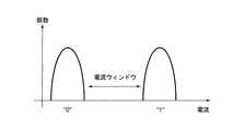
このように、特許文献1に記載された構造の半導体不揮発性メモリは、読み出し電流値の大小によって、2値のデータ“0”・“1”を判別する。この読み出し電流値は、データ“0”・“1”に応じて全てのメモリセルにおいて一定の値を取ることが理想的であるが、実際にはプロセスばらつき等の諸事情からメモリセルごとにある程度のばらつきが生じる。
As described above, the semiconductor nonvolatile memory having the structure described in
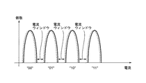
図11は、多数のメモリセルの集合において、読み出し電流値を横軸とし、その読み出し電流値をとるメモリセルの電荷蓄積部の個数を縦軸としたグラフである。このように、データ“0”・“1”それぞれに対応する理想的な電流値を中心とした分布を示す。そして、データ“0”を示す電荷蓄積部の分布とデータ“1”を示す電荷蓄積部の分布との間の、ある程度の幅の電流値の範囲を“電流ウィンドウ”と呼び、書き込まれた“0”と“1”を書き込まれた通りに判別するためには、十分な幅の電流ウィンドウが存在することが必要となる。
そして近年、1つのメモリセルに2つの電荷蓄積部が設けられた半導体不揮発性メモリにおいて、1つのメモリセル当たり4ビットのデータを記憶させることを実現しようという試みがなされ始めている。
FIG. 11 is a graph with the horizontal axis representing the read current value and the vertical axis representing the number of charge storage portions of the memory cell taking the read current value in a set of many memory cells. Thus, the distribution centering on the ideal current value corresponding to each of the data “0” and “1” is shown. A range of a current value having a certain width between the distribution of the charge storage portion indicating data “0” and the distribution of the charge storage portion indicating data “1” is called a “current window” and written “ In order to discriminate 0 ”and“ 1 ”as written, it is necessary that a current window having a sufficient width exists.
In recent years, attempts have been made to realize storage of 4-bit data per memory cell in a semiconductor nonvolatile memory in which two charge storage portions are provided in one memory cell.
例えば非特許文献1では、メモリセルのゲート電極の下側に形成された一の連続したシリコン窒化膜の両端を電荷蓄積部とする構造において、それぞれの電荷蓄積部に4値(“00”,“01”,“10”,“11”)の情報を記憶させることにより、1つのメモリセル当たり4ビットのデータを記憶させることが開示されている。また、セルの2つの端部間のクロストーク(Cross talk)に対処することと、正確な書き込みを行うことが重要であると記載されている。
For example, in Non-Patent
クロストークへの対処としては、それぞれのセルについて同時4ビット書き込みを行うと記載されている。
そして、具体的な書き込み方法として、2段階の書き込みを行うことが記載されている。2段階の書き込みとは、迅速な書き込みを行うための第1段階と、正確な書き込みを行うための第2段階とからなる。第1段階は、所定のドレイン電圧(非特許文献1のFigure4によると3V)から書き込みを開始し、書き込み回数が増えるにつれてドレイン電圧を徐々に上げてゆくドレイン・ステッピング(drain stepping)を行い、それぞれの電荷蓄積部における所望の閾値電圧に達する少し前の時点で書き込みを止める。第2段階は、所定のゲート電圧(非特許文献1のFigure4によると7V)から書き込みを開始し、書き込み回数が増えるにつれてゲート電圧を上げてゆくゲート・ステッピング(gate stepping)を行うことにより、それぞれの電荷蓄積部における所望の閾値電圧とする。この2段階の書き込みによって、書き込みの正確性を向上させることができると記載されている。
As a countermeasure against crosstalk, it is described that simultaneous 4-bit writing is performed for each cell.
As a specific writing method, it is described that two-step writing is performed. The two-stage writing includes a first stage for performing rapid writing and a second stage for performing accurate writing. In the first stage, writing is started from a predetermined drain voltage (3 V according to FIG. 4 of Non-Patent Document 1), and drain stepping is performed to gradually increase the drain voltage as the number of times of writing increases. Write is stopped at a point just before reaching the desired threshold voltage in the charge storage section. In the second stage, writing is started from a predetermined gate voltage (7 V according to FIG. 4 of Non-Patent Document 1), and gate stepping (gate stepping) is performed in which the gate voltage is increased as the number of writing increases. The desired threshold voltage in the charge storage section is set. It is described that the writing accuracy can be improved by this two-step writing.
このように、電圧の印加と書き込み量(又は読み出し電流値)の確認を各電荷蓄積部に対して順次行い、これを複数回繰り返すことで所望の書き込み量(又は読み出し電流値)にする書き込み方法は、「ベリファイ書き込み」と呼ばれることもある。ベリファイ書き込みは、1回の電圧印加によって所望の書き込み量にする方法に比べて、精度良く所望の書き込み量に到達させることができる。 As described above, a writing method in which a voltage is applied and a writing amount (or reading current value) is sequentially confirmed for each charge storage unit, and this is repeated a plurality of times to obtain a desired writing amount (or reading current value). Is sometimes called “verify write”. The verify write can reach the desired write amount with higher accuracy than the method of obtaining the desired write amount by applying a single voltage.
一方、フラッシュメモリ等の不揮発性半導体メモリの書き込みに関して、ワード線ディスターブと呼ばれる問題が知られている(特許文献2)。ワード線ディスターブとは、ワード線を共通にするビットへの書き込み動作に伴い非選択のメモリセルにも高い電圧が印加されて弱い書き込み(ディスターブ)状態が生じ、閾値電圧が変動して記憶データが変化してしまうことをいう。特許文献2では、ワード線ディスターブの問題に対処するために、深い書き込みを要するメモリセルから順に書き込みを行う技術が開示されている。 On the other hand, a problem called word line disturb is known regarding writing in a nonvolatile semiconductor memory such as a flash memory (Patent Document 2). Word line disturb is a weak write (disturb) state caused by a high voltage applied to non-selected memory cells in accordance with a write operation to a bit having a common word line, and the threshold voltage fluctuates to change the stored data. It means changing. Japanese Patent Application Laid-Open No. 2004-228561 discloses a technique for performing writing in order from memory cells that require deep writing in order to cope with the problem of word line disturbance.
1つのメモリセルに2つの電荷蓄積部が設けられた半導体不揮発性メモリにおいては、一の電荷蓄積部への書き込み動作によって、同一メモリセル中の他の電荷蓄積部(「ミラー側」と呼ぶこともある)の読み出し電流値が下がってしまう問題がある。 In a semiconductor nonvolatile memory in which two charge storage units are provided in one memory cell, another charge storage unit (referred to as “mirror side”) in the same memory cell by a write operation to one charge storage unit. There is also a problem that the read current value decreases.
例えば、特許文献1の半導体不揮発性メモリにおいて、1つのメモリセル当たり2ビットのデータを記憶させる場合、すなわち1つの電荷蓄積部に“0”と“1”の2値のデータを記憶させる場合において、1つのメモリセルの2つの電荷蓄積部のうち、一方(例えばソース側)の電荷蓄積部に“0”を、他方(例えばドレイン側)の電荷蓄積部に“1”を記憶させるとする。ソース側に“0”を記憶させるには、ソース側の電荷蓄積部に対して書き込み動作を行い、電荷を蓄積させる必要がある。しかしながら、ソース側の電荷蓄積部に対して書き込み動作を行うと、ドレイン側の読み出し電流値が所望の読み出し電流値よりも低くなってしまうのである。これは、ドレイン側を読み出す動作をすると、ソース側の電荷蓄積部に蓄積された電荷が電流の流れを妨げてしまうことが主な原因であると考えられる。
For example, in the semiconductor nonvolatile memory of
なお、この問題点は、1つのメモリセルに2つの電荷蓄積部が設けられた半導体不揮発性メモリに限らず、1つのメモリセルに3つ以上の電荷蓄積部が設けられた半導体不揮発性メモリについても生じるものである。
図12は、多数のメモリセルの集合において、ミラー側の読み出し電流値が低下した状態を示したグラフである。図11と同様に、読み出し電流値を横軸とし、その読み出し電流値をとるメモリセルの個数を縦軸としたグラフである。また、実線は、同一のメモリセルにおける一の電荷蓄積部への書き込みが行われる前の状態のデータの読み出し電流値の分布であり、破線が、同一のメモリセルにおける一の電荷蓄積部への書き込みが行われた後のミラー側のデータ電流値の分布である。このように、“1”の読み出し電流値が全体的に低下することにより、“0”と“1”の間の電流ウィンドウが狭くなってしまう。
この点、1つのメモリセル当たり2ビットのデータを記憶させる場合であれば、上述のベリファイ書き込みにより書き込みの精度を上げることで読み出し電流値の散らばりを狭めることができ、これによりある程度の電流ウィンドウを確保することができた。
Note that this problem is not limited to a semiconductor nonvolatile memory in which two charge storage units are provided in one memory cell, but in a semiconductor nonvolatile memory in which three or more charge storage units are provided in one memory cell. Will also occur.
FIG. 12 is a graph showing a state in which the read current value on the mirror side is lowered in a set of a large number of memory cells. Similarly to FIG. 11, the horizontal axis represents the read current value, and the vertical axis represents the number of memory cells taking the read current value. The solid line is the distribution of the read current value of the data in the state before writing to one charge storage unit in the same memory cell, and the broken line is the distribution to one charge storage unit in the same memory cell. It is a distribution of data current values on the mirror side after writing is performed. As described above, when the read current value of “1” decreases as a whole, the current window between “0” and “1” becomes narrow.
In this regard, in the case of storing 2 bits of data per memory cell, it is possible to narrow the dispersion of the read current value by increasing the write accuracy by the above-described verify write, and thereby a certain current window can be reduced. I was able to secure it.
しかしながら、1つのメモリセルに2つの電荷蓄積部が設けられた半導体不揮発性メモリにおいて1つのメモリセル当たり4ビットのデータを記憶させる場合、各電荷蓄積部に2ビット(4値)のデータを書き込むことになる。例えば図13は、特許文献1に記載された半導体不揮発性メモリにおいて1つのメモリセル当たり4ビットのデータを記憶させる場合に、メモリセルの各電荷蓄積部が取るべき状態を概念的に示す図である。また、図14は、多数のメモリセルの集合における理想的な読み出し電流値の分布を示すものであり、読み出し電流値を横軸とし、その読み出し電流値をとるメモリセルの個数を縦軸としたグラフである。このように、電流ウィンドウが1つのメモリセル当たり2ビットの場合よりも狭くなる。
However, when storing 4 bits of data per memory cell in a semiconductor nonvolatile memory in which two charge storage units are provided in one memory cell, 2 bits (four values) of data are written in each charge storage unit. It will be. For example, FIG. 13 is a diagram conceptually showing a state that each charge storage unit of a memory cell should take when storing 4-bit data per memory cell in the semiconductor nonvolatile memory described in
このため、図15に示すように、ミラー側の読み出し電流値が低下してしまうと、ベリファイ書き込みを行ったとしても電流ウィンドウを確保することが困難となる。例えば、一方の電荷蓄積部が初期状態である“11”状態である場合の読み出し電流値に着目する。この場合、他方の電荷蓄積部も“11”状態である場合は読み出し電流値の低下は起きないが、他方の電荷蓄積部に“00”データが書き込まれている場合は、一方の電荷蓄積部の読み出し電流値は低下してしまう。このため、“10”と“11”との間の電流ウィンドウが狭くなってしまう。このような現象が各データについて起きるため、十分な電流ウィンドウを確保することが困難となるのである。 For this reason, as shown in FIG. 15, if the read current value on the mirror side decreases, it becomes difficult to secure a current window even if verify writing is performed. For example, attention is focused on the read current value when one charge storage unit is in the “11” state, which is the initial state. In this case, when the other charge storage unit is also in the “11” state, the read current value does not decrease, but when “00” data is written in the other charge storage unit, one charge storage unit Read current value decreases. This narrows the current window between “10” and “11”. Since such a phenomenon occurs for each data, it is difficult to ensure a sufficient current window.
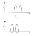
なお、図15において、実線は、同一のメモリセルにおける他方の電荷蓄積部への書き込みが行われる前の一方の電荷蓄積部のデータの読み出し電流値の分布であり、破線が、同一のメモリセルにおける他方の電荷蓄積部への書き込みが行われた後の一方の電荷蓄積部のデータ電流値の分布である。 In FIG. 15, the solid line represents the distribution of the read current value of the data in one charge storage unit before writing to the other charge storage unit in the same memory cell, and the broken line represents the same memory cell. Is a distribution of data current values of one charge storage unit after writing to the other charge storage unit.
特に、従来のベリファイ書き込みでは電荷蓄積部への電荷の蓄積量が多く必要な場合ほど多くの書き込み回数を要する。このため、あるメモリセルの複数の電荷蓄積部それぞれに蓄積されるべき電荷の蓄積量が異なる場合、一の電荷蓄積部への書き込みを行い所望の電流値に達したとしても、その後他の電荷蓄積部への書き込みが続けられることになる。すなわち、それぞれの電荷蓄積部に対する書き込み回数が揃わない。この場合、他の電荷蓄積部へ更に電荷が多く蓄積されたことによって、書き込みが完了し所望の読み出し電流値を示していたはずの一の電荷蓄積部は、他の電荷蓄積部への書き込み完了後は読み出し電流値が減少してしまうことになる。 In particular, in the conventional verify writing, the larger the number of charges stored in the charge storage portion, the more the number of writing is required. For this reason, if the amount of charge to be stored in each of the plurality of charge storage units of a memory cell is different, even if writing to one charge storage unit and reaching a desired current value, another charge is stored thereafter. Writing to the storage unit is continued. That is, the number of times of writing to each charge storage unit is not uniform. In this case, when more charges are accumulated in the other charge accumulating unit, writing is completed and one charge accumulating unit that should have shown the desired read current value has completed writing to the other charge accumulating unit. Thereafter, the read current value decreases.
また、非特許文献1に記載の2段階の書き込みを行ったとしても、書き込み開始電圧が一定である以上、それぞれの電荷蓄積部に対する書き込み回数は揃わない。このため、先に書き込みが完了した電荷蓄積部の読み出し電流値が変化してしまうという問題は解消しない。
従って、従来の書き込み方法では4値のデータを区別することが困難であるという問題があった。
Further, even if the two-stage writing described in
Therefore, the conventional writing method has a problem that it is difficult to distinguish four-value data.
そこで本発明の目的は、1つのメモリセルに複数の電荷蓄積部が設けられた半導体不揮発性メモリにおいて、一の電荷蓄積部への書き込み動作による同一メモリセル中の他の電荷蓄積部の読み出し電流値の低下を抑制することができる、半導体不揮発性メモリ、データ書き込み方法、半導体不揮発性メモリの製造方法、及びデータ書き込みプログラムを提供することにある。 Accordingly, an object of the present invention is to provide a read current of another charge storage portion in the same memory cell by a write operation to one charge storage portion in a semiconductor nonvolatile memory in which a plurality of charge storage portions are provided in one memory cell. It is an object of the present invention to provide a semiconductor nonvolatile memory, a data writing method, a semiconductor nonvolatile memory manufacturing method, and a data writing program capable of suppressing a decrease in value.
そこで、上記問題を解決するために、この発明の代表的な半導体不揮発性メモリは、所定の3値以上のデータを記憶可能な電荷蓄積部を複数備えたメモリセルが複数設けられたメモリセルアレイと、データのうち読み出し電流値がより低い前記データの書き込みのためにはより高い電圧を用いることにより、データを複数のメモリセルの各電荷蓄積部に記憶させる電圧供給部と、書き込みが必要な各電荷蓄積部に対して順次書き込みを行い、データに対応する所定の読み出し電流値に達するまで、書き込みが必要な各電荷蓄積部それぞれにつき書き込みを複数回行うことによりデータを記憶させるように電圧供給部を制御する制御部と、を有する。 In order to solve the above problem, a typical semiconductor nonvolatile memory according to the present invention includes a memory cell array provided with a plurality of memory cells each including a plurality of charge storage portions capable of storing data of a predetermined ternary value or more. A voltage supply unit that stores data in each charge storage unit of a plurality of memory cells by using a higher voltage for writing the data having a lower read current value among the data, and each of the data that needs to be written A voltage supply unit that sequentially writes data to the charge storage unit and stores data by performing multiple writes for each charge storage unit that needs to be written until a predetermined read current value corresponding to the data is reached. And a control unit for controlling.
本発明によれば、1つのメモリセルに複数の電荷蓄積部が設けられた半導体不揮発性メモリにおいて、一の電荷蓄積部への書き込み動作による同一メモリセル中の他の電荷蓄積部の読み出し電流値の低下を抑制することができる。 According to the present invention, in a semiconductor nonvolatile memory in which a plurality of charge storage units are provided in one memory cell, a read current value of another charge storage unit in the same memory cell by a write operation to one charge storage unit Can be suppressed.
以下、図1乃至図9を参照して、この発明の実施形態につき説明する。なお、各図はこの発明が理解できる程度に各構成要素の形状、大きさ及び配置関係を概略的に示してあるに過ぎない。従って、この発明は図示例に限定されるものではない。 Hereinafter, an embodiment of the present invention will be described with reference to FIGS. Each drawing merely schematically shows the shape, size, and arrangement relationship of each component to the extent that the present invention can be understood. Therefore, the present invention is not limited to the illustrated example.
(1)第1実施形態
本発明の第1実施形態に係る半導体不揮発性メモリ、データ書き込み方法、半導体不揮発性メモリの製造方法、及びデータ書き込みプログラムを、図1乃至図7を用いて説明する。
本発明は、所定の3値以上のデータを記憶可能な電荷蓄積部を複数備えたメモリセルを対象とするものであるが、本実施形態では、4値のデータ(“00”、“01”、“10”、“11”)を記憶可能な電荷蓄積部を2つ備えたメモリセルを例にとって説明する。すなわち、本実施形態では、1つのメモリセル当たり4ビットのデータが記憶可能なメモリセルを例にとる。
(1) First Embodiment A semiconductor nonvolatile memory, a data writing method, a method for manufacturing a semiconductor nonvolatile memory, and a data writing program according to a first embodiment of the present invention will be described with reference to FIGS.
The present invention is directed to a memory cell including a plurality of charge storage units capable of storing data having a predetermined ternary value or more. In this embodiment, four-value data (“00”, “01”) is used. , “10”, “11”) will be described as an example of a memory cell provided with two charge storage portions. That is, in this embodiment, a memory cell capable of storing 4 bits of data per memory cell is taken as an example.
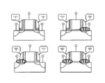
(メモリセルの構造)
図1は、この実施の形態の半導体不揮発性メモリを構成する、メモリセル10の主要部を示す概略断面図である。この実施の形態では、メモリセル10をnMOSFET(n−type Metal Oxide Semiconductor Field Effect Transitor)とした場合を例に挙げて説明する。
(Memory cell structure)
FIG. 1 is a schematic cross-sectional view showing the main part of a
図1に示すように、メモリセル10は、p型半導体基板としてのシリコン基板12の表面領域側に、pウェル領域14が形成されている。このpウェル領域14の表面領域には、n型不純物を高濃度(n+型)に含有するソース領域16及びドレイン領域18が所定距離離間して設けられている。なお、ソース領域16及びドレイン領域18には、それぞれコンタクト層を介して金属電極層が設けられている。これらコンタクト層及び金属電極層は、ソース電極及びドレイン電極をそれぞれ構成する。以下の説明においては、ソース領域及びドレイン領域と称するが、これらは、ソース電極及びドレイン電極とそれぞれ等価である。
As shown in FIG. 1, the
ソース領域16及びドレイン領域18に挟まれる、pウェル領域14上の部分領域には、第1絶縁膜としてのゲート絶縁膜22を介して、制御電極であるゲート電極24が形成されている。ソース領域16及びドレイン領域18に挟まれた、pウェル領域14の表面領域部分が、nMOSFETの動作時にソース・ドレイン領域間のチャネル(電流路)が形成されるチャネル形成領域20となる。ここでのゲート酸化膜は、シリコン酸化膜(SiO2)であり、ゲート電極24は、ポリシリコン(多結晶シリコン)である。なお、上述した、nMOSFETの構造については従来公知であるので、その詳細な説明をここでは省略する。
A
この実施の形態では、ソース領域16とチャネル形成領域20との間に、当該ソース領域16に接して第1抵抗変化部26が設けられている。また、ドレイン領域18とチャネル形成領域20との間に、ドレイン領域18に接して第2抵抗変化部28が設けられている。
In this embodiment, a first
第1及び第2抵抗変化部(26、28)は、それぞれ対応するソース領域16やドレイン領域18よりもn型の不純物濃度が低い(n-型)領域とする。後述する第1及び第2電荷蓄積部(30、32)へ電荷を選択的に注入するために、これら第1及び第2抵抗変化部(26、28)周辺に電界を集中させるためである。その結果、ホットキャリアの発生を抵抗変化部に集中させることができる。なお、抵抗変化部の濃度及び領域の広さ(幅や深さ)は、目的や設計に応じて任意好適に設定することができる。また、これら抵抗変化部(26、28)の構造は、いわゆるLDD(Lightly Doped Drain)と実質的に同様な構造である。
The first and second resistance change sections (26, 28) are regions (n − -type) having a lower n-type impurity concentration than the
さらに、この実施の形態では、第1抵抗変化部26上に第1電荷蓄積部30が設けられており、及び第2抵抗変化部28上に第2電荷蓄積部32が設けられている。
ここでの第1及び第2電荷蓄積部(30、32)は、ONO(Oxide Nitride Oxide)積層絶縁膜である。このONO積層絶縁膜は、第1及び第2抵抗変化部(26、28)上に、シリコン酸化膜(第1酸化膜)301、シリコン窒化膜(SiN)303、及びシリコン酸化膜(第2酸化膜)305が順次積層された構造であり、安定した電荷蓄積機能を有する。
Furthermore, in this embodiment, the first
The first and second charge storage portions (30, 32) here are ONO (Oxide Nitride Oxide) stacked insulating films. The ONO stacked insulating film includes a silicon oxide film (first oxide film) 301, a silicon nitride film (SiN) 303, and a silicon oxide film (second oxide film) on the first and second resistance change portions (26, 28). Film) 305 is sequentially stacked, and has a stable charge storage function.
上述した第1及び第2抵抗変化部(26、28)から注入されたホットキャリアは、このONO積層絶縁膜のうち、主としてシリコン窒化膜303で蓄積される。なお、電荷蓄積部は、構成されるメモリの目的や設計に応じて任意好適に選択可能であり、例えば、シリコン酸化膜等の第1及び第2酸化膜の間に、シリコン窒化膜、酸化アルミニウム膜(Al2O3)及び酸化ハフニウム膜(HfOx)の絶縁膜群のうちから選ばれた一種又は二種以上の絶縁膜が挟まれた構造等を任意好適に選択することができる。
Hot carriers injected from the first and second resistance change sections (26, 28) described above are accumulated mainly in the
この構成例では、第1及び第2電荷蓄積部(30、32)が、第1及び第2抵抗変化部(26、28)上からそれぞれゲート電極24の側壁上にわたって形成されているため、注入された電荷の蓄積・保持が確実になされる。
また、抵抗変化部及び電荷蓄積部は、ソース領域16及びドレイン領域18側の双方にそれぞれ設けてあることにより、第1及び第2電荷蓄積部(30、32)のそれぞれに個別にデータの書き込みが可能である。
In this configuration example, the first and second charge storage portions (30, 32) are formed from the first and second resistance change portions (26, 28) to the side walls of the
In addition, since the resistance change unit and the charge storage unit are provided on both the
さらに、第1及び第2電荷蓄積部(30、32)が、ゲート電極24の両側面の外側に物理的に連続せずに形成されているため、微細化が進みゲート長が短くなったとしても、第1及び第2電荷蓄積部(30、32)それぞれに対して別個独立に電荷を蓄積・保持することができる。
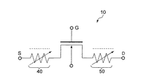
上述した構成を有するメモリセル10の等価回路図を図2に示す。図2に示すように、メモリセル10が具えるnMOSFETを構成する、ソース領域(S)及びドレイン領域(D)側の双方に、第1可変抵抗器40及び第2可変抵抗器50がそれぞれ接続された回路である。
Further, since the first and second charge storage portions (30, 32) are formed on the outside of both side surfaces of the
An equivalent circuit diagram of the
(データの書き込み・読み出し・消去動作)
続いて、表1を参照して、メモリセル10へのデータの書き込み、データの読み出し、及びデータの消去を行う際の動作の概略を説明する。以下では、一例としてメモリセル10のドレイン領域18側に対して、データの書き込み、読み出し及び消去を行う場合につき説明する。なお、ソース領域16側に対して同様の動作を行う場合には、ソース領域及びドレイン領域間の電圧を入れ替えて、同様の動作を行うことができるのは明らかである。
(Data write / read / erase operations)
Next, with reference to Table 1, an outline of operations when data is written to the

<データの書き込み方法>
メモリセル10へのデータの書き込み動作を、例えば、以下の方法で行う。ここでは初期状態を、電荷蓄積部に電荷が蓄積されていない状態(ここでは、論理値“11”に相当)とし、ドレイン領域18側に、論理値“11”以外のデータ、すなわち、論理値“00”、“01”、“10”のいずれかのデータを書き込む場合につき説明する。
ドレイン領域18側にデータを書き込む場合、ドレイン領域18に正電圧(+Vdw)を印加し、ゲート電極24に正電圧(+Vgw)を印加し、ソース領域16を接地電圧とする。
<Data writing method>
The data write operation to the
When data is written on the
こうした条件によって、ドレイン領域18よりもn型不純物濃度の低い第2抵抗変化部28周辺に電界が集中する。よって、第2抵抗変化部28で、衝突電離によるホットキャリアであるホットエレクトロン(高エネルギー電子とも称する。)の発生が効率的に集中する。
Under such conditions, the electric field concentrates around the second
その結果、このホットエレクトロンが、第2抵抗変化部28からシリコン酸化膜301のエネルギー障壁を越えて、第2電荷蓄積部32に選択的に注入されることにより、データの書き込みを行うことができる。
この電圧値+Vdwは、ホットエレクトロンを発生させるのに十分な電圧とし、目的や設計に応じて異なるが、約2V以上、好ましくは、約5〜10V程度とするのが良い。
また、電圧値+Vgwは、チャネル形成領域20に充分なキャリアを形成させ、かつ、ドレイン領域18近傍で発生したホットエレクトロンを第2電荷蓄積部32に注入させるのに十分な電圧とし、目的や設計に応じて異なるが、好ましくは、約3〜12V程度とするのが良い。さらに、この電圧値+Vgwは、書き込むデータの論理値が小さい場合、すなわち読み出し電流値が小さい場合ほど高い電圧とする必要があるが、詳細については後述する。
As a result, the hot electrons are selectively injected from the second
The voltage value + Vdw is a voltage sufficient to generate hot electrons, and varies depending on the purpose and design, but is about 2 V or more, preferably about 5 to 10 V.
Further, the voltage value + Vgw is set to a voltage sufficient to form sufficient carriers in the
<データの読み出し方法>
続いて、ドレイン領域18側のデータの読み出し動作を、以下の方法で行う。
ドレイン領域18側のデータを読み出す場合、ソース領域16に正電圧(+Vsr)を印加し、ゲート電極24に正電圧(+Vgr)を印加し、ドレイン領域18に0または正電圧(+Vdr)を印加とする。
<Data reading method>
Subsequently, the data reading operation on the
When reading data on the
ドレイン領域18側は、第2電荷蓄積部32に電荷(ここでは、電子)が蓄積されている場合、蓄積されている電荷量が多いほど、第2抵抗変化部28の抵抗が上昇する。その結果、チャネル形成領域20にキャリアが供給されにくい状態となり、チャネル形成領域20を流れる電流値が減少する。
On the
一方、ドレイン領域18側が、初期状態である論理値“11”のままである場合は、第2電荷蓄積部32に電荷が蓄積されていないため、第2抵抗変化部28の抵抗は変動しない。その結果、チャネル形成領域20にキャリアが供給され、チャネル形成領域20に十分な電流が流れる。
On the other hand, when the
すなわち、nMOSFETを流れる電流値(読み出し電流値)の違いを利用して、ドレイン領域18側に論理値“00”、“01”、“10”、“11”のいずれのデータが書き込まれているかを判別することができる。
That is, by utilizing the difference in the current value (read current value) flowing through the nMOSFET, which of the logical values “00”, “01”, “10”, “11” is written on the
<情報の記録(消去)方法>
続いて、ドレイン領域18側のデータの消去を、以下の方法で行う。
<Information recording (erasing) method>
Subsequently, the data on the
(a)メモリセル10を、例えば、OTPROM(One Time Programmable Read Only Memory)として用いる場合には、上述した書き込み動作までで終了であるが、良品確認テストの際に書き込んだ情報を消去する必要がある。
この場合には、論理値“00”、“01”又は“10”が書き込まれている、ドレイン領域18側の第2電荷蓄積部32に対して、当該第2電荷蓄積部32に蓄積されている電荷の中和を目的とする、紫外線の照射や加熱処理(高温雰囲気下での放置を含む。)等を行えば良い。このような方法によれば、電気的消去を行うための回路の別途搭載が不要なため、安価なメモリ構成を実現できる。
(A) When the
In this case, the logical value “00”, “01”, or “10” is written in the second
(b)一方、例えば、EEPROM(Electrically Erasable and Programmable ROM)のように、情報を電気的に消去可能な構成とすることも可能である。
この場合には、第2電荷蓄積部32に電荷が蓄積されて帯電している場合(ここでは、論理値“00”、“01”又は“10”が書き込まれている場合)には、ドレイン領域18に正電圧(+Vde)を印加し、ゲート電極24に0または負電圧(−Vge)を印加し、ソース領域16に正電圧(+Vse)を印加する。
(B) On the other hand, it is also possible to adopt a configuration in which information can be electrically erased, such as an EEPROM (Electrically Erasable and Programmable ROM).
In this case, when charge is accumulated in the second charge accumulation unit 32 (here, when the logical value “00”, “01”, or “10” is written), the drain A positive voltage (+ Vde) is applied to the
こうした条件によって、ドレイン領域18周辺で発生したホットホールが、第2電荷蓄積部32に注入される。その結果、第2電荷蓄積部32に蓄積されている電荷(ここでは電子)が中和されることにより、データの消去を行うことができる。なお、このときの+Vdeは、ドレイン領域18近傍で、ホットホールを発生させるのに充分な電圧とし、約2V以上、好ましくは、約4〜10V程度とするのが良い。また、−Vgeは、ホットホールを効率的に第2電荷蓄積部32周辺に集めるために印加する電圧であり、約−7〜0V程度とするのが良い。
Under such conditions, hot holes generated around the
(半導体不揮発性メモリの構成)
続いて、図3を参照して、本実施形態に係る半導体不揮発性メモリ100の構成について以下に説明する。
(Configuration of semiconductor nonvolatile memory)
Next, the configuration of the semiconductor
図3に示すように、半導体不揮発性メモリ100は、メモリセル10が複数設けられたメモリセルアレイ102を備えている。すなわち、メモリセルアレイ102には、第1方向(行方向)に設けられた複数のワード線WLと、第1方向と直交する第2方向(列方向)に複数のビット線BLが交差して配置されており、各ワード線WLと各ビット線BLの交差部にそれぞれメモリセル10が設けられている。
As shown in FIG. 3, the semiconductor
各メモリセル10のゲート電極24は、ワード線WLに接続されている。また、各メモリセル10のソース領域16及びドレイン領域18は、それぞれビット線BLに接続されている。
The
各ワード線WLは、電圧供給部としてのロウデコーダ104に接続されており、各ビット線BLは、電圧供給部としてのカラムデコーダ106に接続されている。このロウデコーダ104及びカラムデコーダ106は、各々制御部としてのコントローラ108に接続されている。
Each word line WL is connected to a
コントローラ108には、メモリセルアレイ102へのデータの書き込み及び読み出し動作を制御する演算部108Aと、データを一時的に記憶する一時記憶部108Bと、後述するデータ書き込みプログラム等の各種プログラムを記憶する不揮発性記憶部108Cと、が設けられている。コントローラ108は、外部よりデータが入力されると、データ書き込みプログラムを実行して、ロウデコーダ104に対して、記憶対象とする2ビットのデータ、当該データの記憶先となるメモリセル10に接続されたワード線WLの行番号を示すロウアドレス、及びワード線WLへ印加する電圧に関する指示情報を出力し、また、カラムデコーダ106に対して、データの記憶先となるメモリセル10に接続された2つのビット線BLの列番号を示すカラムアドレス、及び当該2つのビット線BLへ印加する電圧に関する指示情報を出力する。
The
ロウデコーダ104は、入力した2ビットのデータ、ロウアドレス、及び指示情報に応じてワード線WLへの電圧の印加を制御する。カラムデコーダ106は、入力したカラムアドレス及び指示情報に応じてビット線BLへの電圧の印加を制御する。
(半導体不揮発性メモリの動作)
続いて、本実施形態の半導体不揮発性メモリ100の動作を説明する。
The
(Operation of semiconductor nonvolatile memory)
Next, the operation of the semiconductor
コントローラ108は、外部よりメモリセルアレイ102の各メモリセル10に対して記憶させるデータ(本実施形態では、4ビット構成のデータ)及び記憶先のメモリセル10を指定するアドレスデータが入力されると、当該データ及びアドレスデータを一時記憶部108Bに一旦記憶し、不揮発性記憶部108Cに記憶されているデータ書き込みプログラムを実行する。
When the
データ書き込みプログラムは、各メモリセル10の各電荷蓄積部(30、32)に順次書き込み・読み出しを行い、所望の読み出し電流値以下になるまで各電荷蓄積部(30、32)につき複数回の書き込み・読み出しを繰り返す。
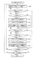
図4は、コントローラ108によって実行されるデータ書き込みプログラムの処理の流れを示すフローチャートである。データ書き込みプログラムの具体的な処理の流れを、図4を用いて以下説明する。
The data writing program sequentially writes / reads data to / from each charge storage unit (30, 32) of each
FIG. 4 is a flowchart showing the flow of processing of the data writing program executed by the
ステップ200では、メモリセルアレイ102の最初のアドレスから順に一時記憶部108Bから1つのメモリセル10に対して記憶させる4ビットのデータを記憶対象のデータとして読み出し、読み出した4ビットデータを上位2ビットと下位2ビットのデータに分割する。
In
次のステップ201では、記憶対象となる上位2ビットのデータが所望のアドレスのメモリセル10において記憶が完了しているかどうかを判断すべく、一時記憶部108Bから、記憶対象となる上位2ビットのデータに関する記憶完了フラグを読み出す。記憶完了フラグが1(記憶未完了)である場合はステップ202へ移行し、記憶完了フラグが0(記憶完了)である場合はステップ207へ移行する。なお、記憶完了フラグの初期値は1(記憶未完了)である(本実施形態について、以下同様)。
In the
次のステップ202では、記憶対象となる上位2ビットのデータが、“11”データであるか、“11”データ以外のデータ(“00”、“01”、“10”)であるかどうかを判定する。記憶対象となる上位2ビットのデータが“11”データである場合は、書き込みの必要がないため、このデータのアドレス情報と共に記憶完了フラグとして0(記憶完了)を一時記憶部108Bに記憶させ、ステップ207へ移行する。他方、記憶対象となる上位2ビットのデータが、“11”データ以外のデータ(“00”、“01”、“10”)である場合は、ステップ203へ移行する。
In the
次のステップ203では、ロウデコーダ104に対して、上位2ビットのデータ、データの記憶先となるメモリセル10の行番号を示すロウアドレス、及びワード線WLへ印加する電圧に関する指示情報を出力すると共に、カラムデコーダ106に対して、データの記憶先となるメモリセル10の列番号を示すカラムアドレス、及びソース領域16に接続されたビット線BLへの電圧の供給を指示する指示情報を出力する。
In the
ロウデコーダ104は、ロウアドレスにより指定された行番号のワード線WLに上位2ビットのデータに応じた正電圧(+Vgw)を所定の書き込み時間だけ印加する。なお、この正電圧(+Vgw)については後述する。
The
カラムデコーダ106は、カラムアドレスにより指定された列番号のドレイン領域18に接続されたビット線BLを接地させると共に、ソース領域16に接続されたビット線BLに正電圧(+Vdw)を所定の書き込み時間だけ印加する。
The
これにより、指定されたメモリセル10のソース領域16に正電圧(+Vdw)が印加され、ゲート電極24に上位2ビットのデータに応じた正電圧(+Vgw)が印加され、ドレイン領域18が接地電圧となり、当該メモリセル10の第1電荷蓄積部30に一定量の電荷が蓄積される。
As a result, a positive voltage (+ Vdw) is applied to the
次のステップ204では、ロウデコーダ104に対して、ステップ203で書き込みを行ったデータの記憶先であるメモリセル10の行番号を示すロウアドレス、及びワード線WLへ印加する電圧に関する指示情報を出力すると共に、カラムデコーダ106に対して、ステップ203で書き込みを行ったデータの記憶先であるメモリセル10の列番号を示すカラムアドレス、及びソース領域16に接続されたビット線BLに0または正電圧の供給を指示する指示情報を出力する。
In the
ロウデコーダ104は、ロウアドレスにより指定された行番号のワード線WLに正電圧(+Vgr)を印加する。
The
カラムデコーダ106は、カラムアドレスにより指定された列番号のドレイン領域18に接続されたビット線BLに正電圧(+Vsr)を印加すると共に、ソース領域16に接続されたビット線BLに0または正電圧(+Vdr)を印加する。
The
これにより、指定されたメモリセル10のソース領域16が接地電圧となるか正電圧(+Vdr)が印加され、ゲート電極24に正電圧(+Vgr)が印加され、ドレイン領域18に正電圧(+Vsr)が印加されるため、当該メモリセル10のドレイン領域18とソース領域16との間に電流が流れる。
As a result, the
次のステップ206では、この読み出し電流値が、ステップ203で書き込み対象となっていたデータに応じた所定の読み出し電流値(以下、「ベリファイ電流値」とも呼ぶ)以下であるかどうかを比較し、読み出し電流値がベリファイ電流値以下である場合はこの電荷蓄積部へのデータの記憶が完了したと判断し、このデータのアドレス情報と共に記憶完了フラグとして0(記憶完了)を一時記憶部108Bに記憶させる。他方、読み出し電流値がベリファイ電流値より大きい場合は、この電荷蓄積部へのデータの記憶が完了していないと判断し、このデータのアドレス情報と共に記憶完了フラグとして1(記憶未完了)を一時記憶部108Bに記憶させる。
In the
次のステップ207では、記憶対象となる下位2ビットのデータが所望のアドレスのメモリセル10において記憶が完了しているかどうかを判断すべく、一時記憶部108Bから、記憶対象となる下位2ビットのデータに関する記憶完了フラグを読み出す。記憶完了フラグが1(記憶未完了)である場合はステップ208へ移行し、記憶完了フラグが0(記憶完了)である場合はステップ214へ移行する。
In the
次のステップ208では、記憶対象となる下位2ビットのデータが、“11”データであるか、“11”データ以外のデータ(“00”、“01”、“10”)であるかどうかを判定する。記憶対象となる下位2ビットのデータが“11”データである場合は、書き込みの必要がないため、このデータのアドレス情報と共に記憶完了フラグとして0(記憶完了)を一時記憶部108Bに記憶させ、ステップ214へ移行する。他方、記憶対象となる下位2ビットのデータが、“11”データ以外のデータ(“00”、“01”、“10”)である場合は、ステップ209へ移行する。
In the
次のステップ209では、ロウデコーダ104に対して、下位2ビットのデータ、データの記憶先となるメモリセル10の行番号を示すロウアドレス、及びワード線WLへ印加する電圧に関する指示情報を出力すると共に、カラムデコーダ106に対して、データの記憶先となるメモリセル10の列番号を示すカラムアドレス、及びソース領域16に接続されたビット線BLの接地を指示する指示情報を出力する。
In the
ロウデコーダ104は、ロウアドレスにより指定された行番号のワード線WLに下位2ビットのデータに応じた正電圧(+Vgw)を所定の書き込み時間だけ印加する。なお、この正電圧(+Vgw)については後述する。
The
カラムデコーダ106は、カラムアドレスにより指定された列番号のドレイン領域18に接続されたビット線BLに正電圧(+Vgw)を所定の書き込み時間だけ印加すると共に、ソース領域16に接続されたビット線BLを接地する。
The
これにより、指定されたメモリセル10のドレイン領域18に正電圧(+Vdw)が印加され、ゲート電極24に下位2ビットのデータに応じた正電圧(+Vgw)が印加され、ソース領域16が接地電圧となり、当該メモリセル10の第2電荷蓄積部32に一定量の電荷が蓄積される。
As a result, a positive voltage (+ Vdw) is applied to the
次のステップ210では、ロウデコーダ104に対して、ステップ209で書き込みを行ったデータの記憶先であるメモリセル10の行番号を示すロウアドレス、及びワード線WLへ印加する電圧に関する指示情報を出力すると共に、カラムデコーダ106に対して、ステップ209で書き込みを行ったデータの記憶先であるメモリセル10の列番号を示すカラムアドレス、及びソース領域16に接続されたビット線BLへの電圧の供給を指示する指示情報を出力する。
In the
ロウデコーダ104は、ロウアドレスにより指定された行番号のワード線WLに正電圧(+Vgr)を印加する。
The
カラムデコーダ106は、カラムアドレスにより指定された列番号のドレイン領域18に接続されたビット線BLに0または正電圧(+Vdr)を印加すると共に、ソース領域16に接続されたビット線BLに正電圧(+Vsr)を印加する。
The
これにより、指定されたメモリセル10のソース領域16に正電圧(+Vsr)が印加され、ゲート電極24に正電圧(+Vgr)が印加され、ドレイン領域18が接地電圧または正電圧(+Vdr)となるため、当該メモリセル10のソース領域16とドレイン領域18との間に電流が流れる。
As a result, a positive voltage (+ Vsr) is applied to the
次のステップ212では、この読み出し電流値が、ステップ209で書き込み対象となっていたデータに応じた所定のベリファイ電流値以下であるかどうかを比較し、読み出し電流値がベリファイ電流値以下である場合はこの電荷蓄積部へのデータの記憶が完了したと判断し、このデータのアドレス情報と共に記憶完了フラグとして0(記憶完了)を一時記憶部108Bに記憶させる。他方、読み出し電流値がベリファイ電流値より大きい場合は、この電荷蓄積部へのデータの記憶が完了していないと判断し、このデータのアドレス情報と共に記憶完了フラグとして1(記憶未完了)を一時記憶部108Bに記憶させる。
In the
次のステップ214では、ステップ200で読み出したデータが、メモリセルアレイ102において記憶対象となる最後のデータであるかどうかを判定し、最後のデータでない場合はステップ200に戻り、最後のデータである場合はステップ216へ移行する。
In the
次のステップ216では、メモリセルアレイ102への記憶対象となるすべてのデータについての記憶完了フラグがすべて0(記憶完了)であるかどうかを判定し、一つでも1(記憶未完了)がある場合はステップ200に戻り、すべて0である場合は本データ書き込みプログラムの処理終了となる。
In the
上述のような書き込み方法において、ステップ203及びステップ209におけるゲート電極24に印加するデータに応じた正電圧(+Vgw)としては、各データ(“00”・“01”・“10”・“11”)のうち読み出し電流値がより低いデータの書き込みのためにはより高い電圧となるようにあらかじめ設定しておく。すなわち、本実施形態では、書き込みの必要がない“11”以外の“00”・“01”・“10”を書き込みの必要があるので、“00”データの書き込みには最も高い電圧値+Vgwを用い、“01”データの書き込みには“00”データの書き込みに用いる電圧値+Vgwよりも低い電圧値+Vgwを用い、“10”データの書き込みには“01”データの書き込みに用いる電圧値+Vgwよりも低い電圧値+Vgwを用いる。
In the writing method as described above, each data (“00”, “01”, “10”, “11”) is used as the positive voltage (+ Vgw) corresponding to the data applied to the
また、さらに望ましくは、ステップ203及びステップ209におけるゲート電極24に印加するデータに応じた正電圧(+Vgw)としては、書き込みが必要となる全ての電荷蓄積部への書き込み回数が同じになるようにあらかじめ設定しておくと良い。すなわち、本実施形態では、書き込みの必要がない“11”以外の“00”・“01”・“10”を書き込みの必要があるので、“00”・“01”・“10”の書き込み回数が同じになるような電圧値+Vgwとする。
More preferably, as the positive voltage (+ Vgw) corresponding to the data applied to the
そうすることによって、書き込みが必要となる全ての電荷蓄積部への書き込み回数を実質的に同じにすることが可能となる。
ここで、書き込み回数を「実質的に」同じにすることができる、と言うことができるにとどまるのは、上述のように書き込みが必要となる全ての電荷蓄積部への書き込み回数が同じになるように+Vgwを設定し、上述のデータ書き込みプログラムにより書き込みを行ったとしても、実際に各データの書き込み回数が同じなることは稀であり、ある程度のばらつきが生じるためである。これは、プロセスばらつきによりメモリセル10の構造にばらつきがあるため、ある回数の書き込みを経た状態において、メモリセルアレイ102中の一の電荷蓄積部は所定のベリファイ電流値以下に達していても、他の電荷蓄積部は未だに所定のベリファイ電流値以下に達しておらず、更なる書き込み動作が必要である、という状況がしばしば発生するためである。
By doing so, it becomes possible to make the number of times of writing to all the charge accumulators that require writing substantially the same.
Here, it can be said that the number of times of writing can be made “substantially” the same. The number of times of writing to all the charge storage units that require writing is the same as described above. Even if + Vgw is set as described above and writing is performed by the above-described data writing program, it is rare that the number of times of writing of each data is actually the same, and some variation occurs. This is because the structure of the
また、本実施形態では、ドレイン電圧+Vdrを一定とし、ゲート電圧+Vgrを記憶対象となるデータに応じて変える(すなわち、読み出し電流値がより低いデータの書き込みのためには+Vgrをより大きくする)ことにより、読み出し電流値がより低いデータの書き込みのためにはより高い電圧を用いることを実現する。この点逆に、ゲート電圧+Vgrを一定とし、ドレイン電圧+Vdrを記憶対象となるデータに応じて変えることにより、読み出し電流値がより低いデータの書き込みのためにはより高い電圧を用いることを実現してもよい。しかしながら、ドレイン電圧の変化量が電荷の蓄積量に与える影響の方が、ゲート電圧の変化量が電荷の蓄積量に与える影響よりも大きいため、ドレイン電圧を記憶対象となるデータに応じて変える方法の方が、調整が難しい。言い換えれば、本実施形態のようにゲート電圧を変化させる方法の方が、電荷の蓄積量を精度良く調整することが可能となる。 In this embodiment, the drain voltage + Vdr is constant, and the gate voltage + Vgr is changed according to data to be stored (that is, + Vgr is increased for writing data with a lower read current value). Thus, it is possible to use a higher voltage for writing data having a lower read current value. Conversely, by using a constant gate voltage + Vgr and changing the drain voltage + Vdr according to the data to be stored, it is possible to use a higher voltage for writing data with a lower read current value. May be. However, since the influence of the change amount of the drain voltage on the charge accumulation amount is larger than the influence of the change amount of the gate voltage on the charge accumulation amount, a method of changing the drain voltage according to the data to be stored Is more difficult to adjust. In other words, the method of changing the gate voltage as in the present embodiment makes it possible to adjust the charge accumulation amount with high accuracy.
また、2回目以降の書き込みを行う場合(すなわち、図4のステップ216で、全データの記憶が完了していないためステップ200に戻り、更に書き込みを行う場合)においては、書き込み回数が増えるごとに書き込み動作に用いる電圧を少しずつ上げても良い。すなわち、電圧値+Vgwを少しずつ上げていくとよい。同じ電圧で書き込みを繰り返すと、精度の良い書き込みを実現することができる反面、所望の読み出し電流値(ベリファイ電流値)に到達するまでに多くの書き込み回数が必要となってしまう場合があるからである。なお、上述のようにゲート電圧を一定にしてドレイン電圧を変化させる方法をとった場合は、書き込み回数が増えるごとにドレイン電圧を少しずつ上げることとなる。
上述のような本実施形態の半導体不揮発性メモリ100の動作を行うための具体的な条件は、例えば次のようなものである。
In addition, in the case of performing the second and subsequent writings (that is, in the case where all data is not stored in
Specific conditions for performing the operation of the semiconductor
まず、ステップ203及びステップ209における書き込み条件は、+Vdwが6.5Vであり、Vswが0Vである。pウェル領域14の電位(基板電位)は+Vswと同じで0Vである。そして+Vgwは、“00”データの書き込みの場合は9V〜11V、“01”データの書き込みの場合は6V〜8V、”10”データの書き込みの場合は5V〜7Vの範囲で、読み出し電流値がより低いデータの書き込みのためにはより高い電圧を用いるように(すなわち、“00”データの書き込み電圧>“01”データの書き込み電圧>“10”データの書き込み電圧、となるように)設定する。なお、本実施形態のように、書き込み電圧としてドレイン電圧を一定にしてゲート電圧を変化させる方法をとる場合は、5Vから11Vという広い範囲で変化させることが可能であるが、上述のようにゲート電圧を一定にしてドレイン電圧を変化させる方法をとる場合には、ドレイン電圧を例えば5Vから7Vという狭い範囲で変化させて調整する必要が生じる。
First, the write condition in
また、1回の書き込み時間は、いずれのデータの場合も500nsecである。さらに、各電荷蓄積部における2回目以降の書き込みにおいては、+Vgwを0.1Vずつ上げていく(但し、上限を12Vとする)。なお、上述のようにゲート電圧を一定にしてドレイン電圧を変化させる方法をとる場合には、ドレイン電圧を例えば0.05Vずつ上げていくというように、小さい数値とする必要がある。
このようにして、いずれのデータにおいても各電化蓄積部当たり合計30回程度の書き込み回数(すなわち、合計15μsec程度の書き込み時間)により記憶完了となるように設定するのが好適である。
The write time for one time is 500 nsec for any data. Further, in the second and subsequent writings in each charge storage unit, + Vgw is increased by 0.1 V (however, the upper limit is set to 12 V). Note that when the method of changing the drain voltage while keeping the gate voltage constant as described above, the drain voltage needs to be set to a small value, for example, by 0.05V.
In this way, it is preferable to set the storage to be completed with the total number of writes of about 30 times (that is, the total write time of about 15 μsec) for each data storage unit in any data.
次に、ステップ204及びステップ210における読み出し条件は、+Vsrが2.0Vであり、+Vgrが3.6Vであり、+Vdwが0.1Vである。pウェル領域14の電位(基板電位)は0Vである。
次に、ステップ206及びステップ212におけるベリファイ電流値は、“00”データの場合は15μA〜20μA、“01”データの場合は25μA〜30μA、“10”データの場合は35μA〜40μAである。より具体的には、“00”データの場合は15μA、“01”データの場合は27μA、“10”データの場合は39μAとするのが良い。
Next, the reading conditions in
Next, the verify current values in
(第1実施形態の効果)
以上のように、本実施形態によれば、読み出し電流値がより低いデータの書き込みのためにはより高い電圧を用い、メモリセルアレイ102中のすべてのメモリセル10の書き込みが必要な各電荷蓄積部(30、32)に対して順次書き込みを行い、各データに対応する所定の読み出し電流値(ベリファイ電流値)に達するまで、書き込みが必要な各電荷蓄積部(30、32)それぞれにつき書き込みを複数回行うことにより各データを記憶させるため、書き込みが必要となる各電荷蓄積部(30、32)への書き込み回数の差を小さくすることができる。このため、各データの所望の読み出し電流値からのずれを少なくできる。従って、図5に示すように、4値のデータを判別するために必要な電流ウィンドウを確保することができる。
(Effect of 1st Embodiment)
As described above, according to the present embodiment, each charge storage unit that uses a higher voltage to write data with a lower read current value and needs to write all the
図5において、実線は、同一のメモリセル10における他の電荷蓄積部への書き込みが行われていないデータの読み出し電流値の分布であり、破線は、同一のメモリセル10における他の電荷蓄積部への書き込みが行われているデータの読み出し電流値の分布である。書き込み回数の差を小さくしたことにより、同一のメモリセル10における他の電荷蓄積部に行われた書き込みよる一の電荷蓄積部の読み出し電流値の低下を抑制することができる。なお、本発明において「電流ウィンドウ」とは、図5のような、メモリセルアレイ102中の複数のメモリセル10の各電荷蓄積部(30、32)に記憶された各データの読み出し電流値の分布を示すグラフにおいて、各データの分布の間の電流値の範囲をいう。
In FIG. 5, the solid line is the distribution of the read current value of data that has not been written to other charge storage units in the
特に、メモリセルアレイ102中のすべてのメモリセル10の各電荷蓄積部(30、32)の書き込みに用いる電圧を、書き込みが必要となる各電荷蓄積部(30、32)への書き込み回数が同じになるように設定すれば、書き込みが必要となる各電荷蓄積部(30、32)への書き込み回数の差をさらに小さくすることができる(あるいは、上述の通り、理想的には書き込み回数の差をなくすことができる)。
In particular, the voltage used for writing to each of the charge storage units (30, 32) of all the
また、本実施形態の各電荷蓄積部(30、32)における2回目以降の書き込みにおいては、書き込みに用いる電圧を少しずつ上げていく場合、少ない書き込み回数で効率的に所望の読み出し電流値(ベリファイ電流値)に到達することができる。
本実施形態の半導体不揮発性メモリ100における書き込み方法は上述の通りであるが、一つのメモリセル10に着目した場合、次のように捉えることができる。
メモリセル10の2つの電荷蓄積部(30、32)両方に対して書き込みが必要となる場合、すなわち、当該メモリセル10に対する記憶対象となるデータが、“00”・“01”・“10”のうちいずれかの組み合わせである場合、読み出し電流値がより低いデータの書き込みのためにはより高い電圧を用い、各電荷蓄積部それぞれが所定のベリファイ電流値に達するまで2つの電荷蓄積部に対して交互に書き込みが行われることとなる。また、1つの電荷蓄積部に着目すると、電圧の供給は複数回行われることとなる。
Further, in the second and subsequent writings in the charge storage units (30, 32) of the present embodiment, when the voltage used for writing is increased little by little, a desired read current value (verification) can be efficiently performed with a small number of writings. Current value) can be reached.
The writing method in the semiconductor
When writing is required for both of the two charge storage portions (30, 32) of the
例えば、図6は、一の電荷蓄積部に“01”を、他の電荷蓄積部に“10”が記憶される複数のメモリセル10の状況を示すものである。図6(a)は、当該複数のメモリセル10の2つの電荷蓄積部に対して、交互に複数回の書き込みが行われている途中の状態を示すものである。左側の分布が“01”データが書き込まれる途中の状態であり、右側の分布が“10”データが書き込まれる途中の状態である。これらの分布は、交互に少しずつ左側に移動して行く。図6(b)は、当該複数のメモリセル10の2つの電荷蓄積部に対して、“01”データと“10”データの記憶が完了した状態を示すものである。なお、実線は、同一のメモリセル10における他の電荷蓄積部への書き込みが行われていないと仮定した場合のデータの読み出し電流値の分布であり、破線が、図6(a)の書き込みが完了した場合のデータの読み出し電流値の分布である。書き込み回数の差を小さくしたことにより、同一のメモリセル10における他の電荷蓄積部に行われた書き込みよる読み出し電流値の低下を抑制することができるため、電流ウィンドウを確保することができる。
(第1実施形態の第1変形例)
次に、本発明の第1実施形態の第1変形例について説明する。
For example, FIG. 6 shows a situation of a plurality of
(First modification of the first embodiment)
Next, a first modification of the first embodiment of the present invention will be described.
この変形例においては、データ書き込みプログラムを実行する前に、メモリセルアレイ102中の全てのメモリセル10の各電荷蓄積部(30、32)に対して消去動作を実行する。
In this modified example, before the data write program is executed, an erase operation is executed on each charge storage portion (30, 32) of all the
具体的には、−Vgeが−6V、+Vdeが6V、+Vseが6Vであり、pウェル領域14の電位(基板電位)は0Vである。このような電圧を、2msecの時間印加する。
Specifically, -Vge is -6V, + Vde is 6V, + Vse is 6V, and the potential (substrate potential) of the p-
これにより、各電荷蓄積部(30、32)にホットホールが注入されるため、図7に示すように、初期状態(“11”データに対応)の読み出し電流値を上げることができる。このため、各データ間の電流ウィンドウをより広げることができる。 As a result, hot holes are injected into each of the charge storage units (30, 32), so that the read current value in the initial state (corresponding to “11” data) can be increased as shown in FIG. For this reason, the current window between each data can be further expanded.
なお、データ書き込みプログラムに、上述のような消去動作を含めても良い。具体的には、ステップ200の前に、メモリセルアレイ102中のすべてのメモリセル10の各電荷蓄積部(30、32)に対して消去動作を実行するステップを設ければ良い。
(第1実施形態の第2変形例)
次に、本発明の第1実施形態の第2変形例について説明する。
Note that the data write program may include the erase operation as described above. Specifically, a step of executing an erasing operation on each charge storage portion (30, 32) of all the
(Second modification of the first embodiment)
Next, a second modification of the first embodiment of the present invention will be described.
本発明の第1実施形態においては、各電荷蓄積部(30、32)における2回目以降の書き込みにおいては、書き込み回数が1回増えるごとにゲート電圧Vgwを0.1Vずつ上げた。この点を、本発明の第1実施形態の第2変形例においては、書き込み電圧の増加分を0.5Vのように大きくすることで書き込み電圧を早く上昇させ、上昇させた書き込み電圧における書き込みを多く繰り返す。例えば、1回目の書き込み電圧が9Vの場合、2回目は9.5V、3回目は10Vとし、4回目以降は10Vで書き込みを繰り返す。 In the first embodiment of the present invention, the gate voltage Vgw is increased by 0.1 V each time the number of times of writing is increased in the second and subsequent writings in the charge storage units (30, 32). With respect to this point, in the second modification of the first embodiment of the present invention, the write voltage is quickly increased by increasing the increase of the write voltage to 0.5 V, and writing at the increased write voltage is performed. Repeat many times. For example, when the first write voltage is 9V, the second write is 9.5V, the third is 10V, and the fourth and subsequent writes are repeated at 10V.
このような書き込み方法によれば、書き込み回数が少ない段階から1回の書き込み動作による電荷の蓄積量を多くすることができるため、少ない書き込み回数で効率的にデータの記憶を完了させることができる。本発明の第1実施形態のように、0.1Vずつ電圧を上げる方が書き込みの精度を上げることができるが、書き込み回数が制限されるような場合や、より短時間での書き込みが必要となる場合には、この第1実施形態の第2変形例の方法が特に有効である。 According to such a writing method, it is possible to increase the amount of charge accumulated by one writing operation from the stage where the number of times of writing is small, so that data storage can be completed efficiently with a small number of times of writing. As in the first embodiment of the present invention, increasing the voltage by 0.1 V can improve the writing accuracy. However, when the number of times of writing is limited or writing in a shorter time is required. In this case, the method of the second modification of the first embodiment is particularly effective.
(2)第2実施形態
本発明の第2実施形態に係る半導体不揮発性メモリ、データ書き込み方法、半導体不揮発性メモリの製造方法、及びデータ書き込みプログラムを、図8乃至図9を用いて説明する。なお、第1実施形態において説明した構成要素と同じ構成要素については、同一の符号を付してその説明を省略する。
本実施形態のメモリセルの構造、メモリセルへのデータの書き込み・読み出し・消去動作、及び半導体不揮発性メモリの構成は、本発明の第1実施形態におけるものと同様であるので、説明は省略する。
(2) Second Embodiment A semiconductor nonvolatile memory, data writing method, semiconductor nonvolatile memory manufacturing method, and data writing program according to a second embodiment of the present invention will be described with reference to FIGS. In addition, about the same component as the component demonstrated in 1st Embodiment, the same code | symbol is attached | subjected and the description is abbreviate | omitted.
Since the structure of the memory cell, the data write / read / erase operation to the memory cell, and the configuration of the semiconductor nonvolatile memory according to the present embodiment are the same as those in the first embodiment of the present invention, the description thereof is omitted. .
本実施形態は、まず読み出し電流値が最も低いデータである“00”データを全て記憶させ(第1ステップ)、次に、“00”データ以外のデータのうち書き込みが必要となるデータである、“01”データと“10”データを、第1実施形態と同様の方法で全て記憶させる(第2ステップ)ものである。
以下、本実施形態の半導体不揮発性メモリの動作、特に、データ書き込みプログラムの動作について説明する。
In the present embodiment, first, all “00” data, which is data having the lowest read current value, is stored (first step), and next, data that needs to be written out of data other than “00” data. All “01” data and “10” data are stored in the same manner as in the first embodiment (second step).
The operation of the semiconductor nonvolatile memory according to the present embodiment, particularly the operation of the data write program will be described below.
コントローラ108は、外部よりメモリセルアレイ102の各メモリセル10に対して記憶させるデータ(本実施形態では、4ビット構成のデータ)及び記憶先のメモリセル10を指定するアドレスデータが入力されると、当該データ及びアドレスデータを一時記憶部108Bに一旦記憶し、以下のデータ書き込みプログラムを実行する。
図8(a)及び(b)は、コントローラ108によって実行される、本実施形態に係るデータ書き込みプログラムの処理の流れを示すフローチャートである。データ書き込みプログラムの具体的な処理の流れを、図8(a)及び(b)を用いて以下説明する。
When the
FIGS. 8A and 8B are flowcharts showing the flow of processing of the data writing program according to the present embodiment, which is executed by the
ステップ300では、メモリセルアレイ102の最初のアドレスから順に一時記憶部108Bから1つのメモリセル10に対して記憶させる4ビットのデータを記憶対象のデータとして読み出し、読み出した4ビットデータを上位2ビットと下位2ビットのデータに分割する。
In
次のステップ301では、記憶対象となる上位2ビットのデータが所望のアドレスのメモリセル10において記憶が完了しているかどうかを判断すべく、一時記憶部108Bから、記憶対象となる上位2ビットのデータに関する記憶完了フラグを読み出す。記憶完了フラグが1(記憶未完了)である場合はステップ302へ移行し、記憶完了フラグが0(記憶完了)である場合はステップ307へ移行する。なお、記憶完了フラグの初期値は1(記憶未完了)である(本実施形態について、以下同様)。
In the
次のステップ302では、記憶対象となる上位2ビットのデータが、“00”データであるか、“00”データ以外のデータ(“01”、“10”、“11”)であるかどうかを判定する。記憶対象となる上位2ビットのデータが“00”データ以外のデータである場合は、この段階では書き込みの必要がないため、このままステップ307へ移行する。他方、記憶対象となる上位2ビットのデータが、“00”データである場合は、ステップ303へ移行する。
In the
次のステップ303では、ロウデコーダ104に対して、上位2ビットのデータ(ここでは“00”データ)、データの記憶先となるメモリセル10の行番号を示すロウアドレス、及びワード線WLへ印加する電圧に関する指示情報を出力すると共に、カラムデコーダ106に対して、データの記憶先となるメモリセル10の列番号を示すカラムアドレス、及びソース領域16に接続されたビット線BLへの電圧の供給を指示する指示情報を出力する。
In the
ロウデコーダ104は、ロウアドレスにより指定された行番号のワード線WLに上位2ビットのデータに応じた正電圧(+Vgw)を所定の書き込み時間だけ印加する。なお、この正電圧(+Vgw)については後述する。
The
カラムデコーダ106は、カラムアドレスにより指定された列番号のドレイン領域18に接続されたビット線BLを接地させると共に、ソース領域16に接続されたビット線BLに正電圧(+Vdw)を所定の書き込み時間だけ印加する。
The
これにより、指定されたメモリセル10のソース領域16に正電圧(+Vdw)が印加され、ゲート電極24に上位2ビットのデータに応じた正電圧(+Vgw)が印加され、ドレイン領域18が接地電圧となり、当該メモリセル10の第1電荷蓄積部30に一定量の電荷が蓄積される。
As a result, a positive voltage (+ Vdw) is applied to the
次のステップ304では、ロウデコーダ104に対して、ステップ303で書き込みを行ったデータの記憶先であるメモリセル10の行番号を示すロウアドレス、及びワード線WLへ印加する電圧に関する指示情報を出力すると共に、カラムデコーダ106に対して、ステップ303で書き込みを行ったデータの記憶先であるメモリセル10の列番号を示すカラムアドレス、及びソース領域16に接続されたビット線BLに0または正電圧の供給を指示する指示情報を出力する。
In the
ロウデコーダ104は、ロウアドレスにより指定された行番号のワード線WLに正電圧(+Vgr)を印加する。
The
カラムデコーダ106は、カラムアドレスにより指定された列番号のドレイン領域18に接続されたビット線BLに正電圧(+Vsr)を印加すると共に、ソース領域16に接続されたビット線BLに0または正電圧(+Vdr)を印加する。
The
これにより、指定されたメモリセル10のソース領域16が接地電圧となるか正電圧(+Vdr)が印加され、ゲート電極24に正電圧(+Vgr)が印加され、ドレイン領域18に正電圧(+Vsr)が印加されるため、当該メモリセル10のドレイン領域18とソース領域16との間に電流が流れる。
As a result, the
次のステップ306では、この読み出し電流値が、ステップ303で書き込み対象となっていたデータ(ここでは“00”データ)に応じた所定のベリファイ電流値以下であるかどうかを比較し、読み出し電流値がベリファイ電流値以下である場合はこの電荷蓄積部へのデータの記憶が完了したと判断し、このデータのアドレス情報と共に記憶完了フラグとして0(記憶完了)を一時記憶部108Bに記憶させる。他方、読み出し電流値がベリファイ電流値より大きい場合は、この電荷蓄積部へのデータの記憶が完了していないと判断し、このデータのアドレス情報と共に記憶完了フラグとして1(記憶未完了)を一時記憶部108Bに記憶させる。
In the
次のステップ307では、記憶対象となる下位2ビットのデータが所望のアドレスのメモリセル10において記憶が完了しているかどうかを判断すべく、一時記憶部108Bから、記憶対象となる下位2ビットのデータに関する記憶完了フラグを読み出す。記憶完了フラグが1(記憶未完了)である場合はステップ308へ移行し、記憶完了フラグが0(記憶完了)である場合はステップ314へ移行する。
In the
次のステップ308では、記憶対象となる下位2ビットのデータが、“00”データであるか、“00”データ以外のデータ(“01”、“10”、“11”)であるかどうかを判定する。記憶対象となる下位2ビットのデータが“00”データ以外のデータである場合は、この段階では書き込みの必要がないため、このままステップ314へ移行する。他方、記憶対象となる下位2ビットのデータが、“00”データである場合は、ステップ309へ移行する。
In the
次のステップ309では、ロウデコーダ104に対して、下位2ビットのデータ(ここでは“00”データ)、データの記憶先となるメモリセル10の行番号を示すロウアドレス、及びワード線WLへ印加する電圧に関する指示情報を出力すると共に、カラムデコーダ106に対して、データの記憶先となるメモリセル10の列番号を示すカラムアドレス、及びソース領域16に接続されたビット線BLの接地を指示する指示情報を出力する。
In the
ロウデコーダ104は、ロウアドレスにより指定された行番号のワード線WLに下位2ビットのデータに応じた正電圧(+Vgw)を所定の書き込み時間だけ印加する。なお、この正電圧(+Vgw)については後述する。
The
カラムデコーダ106は、カラムアドレスにより指定された列番号のドレイン領域18に接続されたビット線BLに正電圧(+Vgw)を所定の書き込み時間だけ印加すると共に、ソース領域16に接続されたビット線BLを接地する。
The
これにより、指定されたメモリセル10のドレイン領域18に正電圧(+Vdw)が印加され、ゲート電極24に下位2ビットのデータに応じた正電圧(+Vgw)が印加され、ソース領域16が接地電圧となり、当該メモリセル10の第2電荷蓄積部32に一定量の電荷が蓄積される。
As a result, a positive voltage (+ Vdw) is applied to the
次のステップ310では、ロウデコーダ104に対して、ステップ309で書き込みを行ったデータの記憶先であるメモリセル10の行番号を示すロウアドレス、及びワード線WLへ印加する電圧に関する指示情報を出力すると共に、カラムデコーダ106に対して、ステップ309で書き込みを行ったデータの記憶先であるメモリセル10の列番号を示すカラムアドレス、及びソース領域16に接続されたビット線BLへの電圧の供給を指示する指示情報を出力する。
In the
ロウデコーダ104は、ロウアドレスにより指定された行番号のワード線WLに正電圧(+Vgr)を印加する。
The
カラムデコーダ106は、カラムアドレスにより指定された列番号のドレイン領域18に接続されたビット線BLに0または正電圧(+Vdr)を印加すると共に、ソース線SLに正電圧(+Vsr)を印加する。
The
これにより、指定されたメモリセル10のソース領域16が正電圧(+Vsr)となり、ゲート電極24に正電圧(+Vgr)が印加され、ドレイン領域18が接地電圧または正電圧(+Vdr)となるため、当該メモリセル10のソース領域16とドレイン領域18との間に電流が流れる。
As a result, the
次のステップ312では、この読み出し電流値が、ステップ309で書き込み対象となっていたデータに応じた所定のベリファイ電流値以下であるかどうかを比較し、読み出し電流値がベリファイ電流値以下である場合はこの電荷蓄積部へのデータの記憶が完了したと判断し、このデータのアドレス情報と共に記憶完了フラグとして0(記憶完了)を一時記憶部108Bに記憶させる。他方、読み出し電流値がベリファイ電流値より大きい場合は、この電荷蓄積部へのデータの記憶が完了していないと判断し、このデータのアドレス情報と共に記憶完了フラグとして1(記憶未完了)を一時記憶部108Bに記憶させる。
In the
次のステップ314では、ステップ300で読み出したデータが、メモリセルアレイ102において記憶対象となる最後のデータであるかどうかを判定し、最後のデータでない場合はステップ300に戻り、最後のデータである場合はステップ316へ移行する。
In the
次のステップ316では、メモリセルアレイ102への記憶対象となるすべてのデータのうち、すべての“00”データについての記憶完了フラグがすべて0(記憶完了)であるかどうかを判定し、一つでも1(記憶未完了)がある場合はステップ300に戻り、すべて0である場合はステップ400へ移行する。
ステップ400では、メモリセルアレイ102の最初のアドレスから順に一時記憶部108Bから1つのメモリセル10に対して記憶させる4ビットのデータを記憶対象のデータとして読み出し、読み出した4ビットデータを上位2ビットと下位2ビットのデータに分割する。
In the
In
次のステップ401では、記憶対象となる上位2ビットのデータが所望のアドレスのメモリセル10において記憶が完了しているかどうかを判断すべく、一時記憶部108Bから、記憶対象となる上位2ビットのデータに関する記憶完了フラグを読み出す。記憶完了フラグが1(記憶未完了)である場合はステップ402へ移行し、記憶完了フラグが0(記憶完了)である場合はステップ407へ移行する。なお、記憶対象となる上位2ビットのデータが“00”データである場合は既に記憶が完了しており、必ず記憶完了フラグが0となっているため、ステップ407へ移行することとなる。
In the
次のステップ402では、記憶対象となる上位2ビットのデータが、“11”データであるか、“11”データ以外のデータ(ここでは“01”、“10”)であるかどうかを判定する。記憶対象となる上位2ビットのデータが“11”データである場合は、書き込みの必要がないため、このデータのアドレス情報と共に記憶完了フラグとして0(記憶完了)を一時記憶部108Bに記憶させ、ステップ407へ移行する。他方、記憶対象となる上位2ビットのデータが、“11”データ以外のデータ(ここでは“01”、“10”)である場合は、ステップ403へ移行する。
In the
次のステップ403では、ロウデコーダ104に対して、上位2ビットのデータ、データの記憶先となるメモリセル10の行番号を示すロウアドレス、及びワード線WLへ印加する電圧に関する指示情報を出力すると共に、カラムデコーダ106に対して、データの記憶先となるメモリセル10の列番号を示すカラムアドレス、及びソース領域16に接続されたビット線BLへの電圧の供給を指示する指示情報を出力する。
In the
ロウデコーダ104は、ロウアドレスにより指定された行番号のワード線WLに上位2ビットのデータに応じた正電圧(+Vgw)を所定の書き込み時間だけ印加する。なお、この正電圧(+Vgw)については後述する。
The
カラムデコーダ106は、カラムアドレスにより指定された列番号のドレイン領域18に接続されたビット線BLを接地させると共に、ソース領域16に接続されたビット線BLに正電圧(+Vdw)を所定の書き込み時間だけ印加する。
The
これにより、指定されたメモリセル10のソース領域16に正電圧(+Vdw)が印加され、ゲート電極24に上位2ビットのデータに応じた正電圧(+Vgw)が印加され、ドレイン領域18が接地電圧となり、当該メモリセル10の第1電荷蓄積部30に一定量の電荷が蓄積される。
次のステップ404では、ロウデコーダ104に対して、ステップ403で書き込みを行ったデータの記憶先であるメモリセル10の行番号を示すロウアドレス、及びワード線WLへ印加する電圧に関する指示情報を出力すると共に、カラムデコーダ106に対して、ステップ403で書き込みを行ったデータの記憶先であるメモリセル10の列番号を示すカラムアドレス、及びソース領域16に接続されたビット線BLに0または正電圧の供給を指示する指示情報を出力する。
As a result, a positive voltage (+ Vdw) is applied to the
In the
ロウデコーダ104は、ロウアドレスにより指定された行番号のワード線WLに正電圧(+Vgr)を印加する。
The
カラムデコーダ106は、カラムアドレスにより指定された列番号のドレイン領域18に接続されたビット線BLに正電圧(+Vsr)を印加すると共に、ソース領域16に接続されたビット線BLに0または正電圧(+Vdr)を印加する。
The
これにより、指定されたメモリセル10のソース領域16が接地電圧となるか正電圧(+Vdr)が印加され、ゲート電極24に正電圧(+Vgr)が印加され、ドレイン領域18に正電圧(+Vsr)が印加されるため、当該メモリセル10のドレイン領域18とソース領域16との間に電流が流れる。
As a result, the
次のステップ406では、この読み出し電流値が、ステップ403で書き込み対象となっていたデータに応じた所定のベリファイ電流値以下であるかどうかを比較し、読み出し電流値がベリファイ電流値以下である場合はこの電荷蓄積部へのデータの記憶が完了したと判断し、このデータのアドレス情報と共に記憶完了フラグとして0(記憶完了)を一時記憶部108Bに記憶させる。他方、読み出し電流値がベリファイ電流値より大きい場合は、この電荷蓄積部へのデータの記憶が完了していないと判断し、このデータのアドレス情報と共に記憶完了フラグとして1(記憶未完了)を一時記憶部108Bに記憶させる。
In the
次のステップ407では、記憶対象となる下位2ビットのデータが所望のアドレスのメモリセル10において記憶が完了しているかどうかを判断すべく、一時記憶部108Bから、記憶対象となる下位2ビットのデータに関する記憶完了フラグを読み出す。記憶完了フラグが1(記憶未完了)である場合はステップ408へ移行し、記憶完了フラグが0(記憶完了)である場合はステップ414へ移行する。なお、記憶対象となる下位2ビットのデータが”00”データである場合は既に記憶が完了しており、必ず記憶完了フラグが0となっているため、ステップ414へ移行することとなる。
In the
次のステップ408では、記憶対象となる下位2ビットのデータが、“11”データであるか、“11”データ以外のデータ(ここでは“01”、“10”)であるかどうかを判定する。記憶対象となる下位2ビットのデータが“11”データである場合は、書き込みの必要がないため、このデータのアドレス情報と共に記憶完了フラグとして0(記憶完了)を一時記憶部108Bに記憶させ、ステップ414へ移行する。他方、記憶対象となる下位2ビットのデータが、“11”データ以外のデータ(ここでは“01”、“10”)である場合は、ステップ409へ移行する。
In the
次のステップ409では、ロウデコーダ104に対して、下位2ビットのデータ、データの記憶先となるメモリセル10の行番号を示すロウアドレス、及びワード線WLへ印加する電圧に関する指示情報を出力すると共に、カラムデコーダ106に対して、データの記憶先となるメモリセル10の列番号を示すカラムアドレス、及びソース領域16に接続されたビット線BLの接地を指示する指示情報を出力する。
In the
ロウデコーダ104は、ロウアドレスにより指定された行番号のワード線WLに下位2ビットのデータに応じた正電圧(+Vgw)を所定の書き込み時間だけ印加する。なお、この正電圧(+Vgw)については後述する。
The
カラムデコーダ106は、カラムアドレスにより指定された列番号のドレイン領域18に接続されたビット線BLに正電圧(+Vgw)を所定の書き込み時間だけ印加すると共に、ソース領域16に接続されたビット線BLを接地する。
The
これにより、指定されたメモリセル10のドレイン領域18に正電圧(+Vdw)が印加され、ゲート電極24に下位2ビットのデータに応じた正電圧(+Vgw)が印加され、ソース領域16が接地電圧となり、当該メモリセル10の第2電荷蓄積部32に一定量の電荷が蓄積される。
As a result, a positive voltage (+ Vdw) is applied to the
次のステップ410では、ロウデコーダ104に対して、ステップ409で書き込みを行ったデータの記憶先であるメモリセル10の行番号を示すロウアドレス、及びワード線WLへ印加する電圧に関する指示情報を出力すると共に、カラムデコーダ106に対して、ステップ409で書き込みを行ったデータの記憶先であるメモリセル10の列番号を示すカラムアドレス、及びソース領域16に接続されたビット線BLへの電圧の供給を指示する指示情報を出力する。
In the
ロウデコーダ104は、ロウアドレスにより指定された行番号のワード線WLに正電圧(+Vgr)を印加する。
The
カラムデコーダ106は、カラムアドレスにより指定された列番号のビット線BLを接地すると共に、ソース領域16に接続されたビット線BLに正電圧(+Vsr)を印加する。
The
これにより、指定されたメモリセル10のソース領域16に正電圧(+Vsr)が印加され、ゲート電極24に正電圧(+Vgr)が印加され、ドレイン領域18が接地電圧または正電圧(+Vdr)となるため、当該メモリセル10のソース領域16とドレイン領域18との間に電流が流れる。
As a result, a positive voltage (+ Vsr) is applied to the
次のステップ412では、この読み出し電流値が、ステップ409で書き込み対象となっていたデータに応じた所定のベリファイ電流値以下であるかどうかを比較し、読み出し電流値がベリファイ電流値以下である場合はこの電荷蓄積部へのデータの記憶が完了したと判断し、このデータのアドレス情報と共に記憶完了フラグとして0(記憶完了)を一時記憶部108Bに記憶させる。他方、読み出し電流値がベリファイ電流値より大きい場合は、この電荷蓄積部へのデータの記憶が完了していないと判断し、このデータのアドレス情報と共に記憶完了フラグとして1(記憶未完了)を一時記憶部108Bに記憶させる。
In the
次のステップ414では、ステップ400で読み出したデータが、メモリセルアレイ102において記憶対象となる最後のデータであるかどうかを判定し、最後のデータでない場合はステップ400に戻り、最後のデータである場合はステップ416へ移行する。
In the
次のステップ416では、メモリセルアレイ102への記憶対象となるすべてのデータのうち、“00”データ以外のすべてのデータについての記憶完了フラグがすべて0(記憶完了)であるかどうかを判定し、一つでも1(記憶未完了)がある場合はステップ400に戻り、すべて0である場合は本データ書き込みプログラムの処理終了となる。
In the
以上のように、ステップ300〜316においてまず“00”データをすべて記憶させ(第1ステップ)、次に、ステップ400〜416において“01”データと“10”データをすべて記憶させる(第2ステップ)。
As described above, all “00” data is first stored in
上述のような書き込み方法において、読み出し電流値が最も低いデータである“00”データ以外のデータのうち、書き込みが必要となるデータ(すなわち、“01”データと“10”データ)を書き込む際の電圧は、読み出し電流値がより低いデータの書き込みのためにはより高い電圧となるようにあらかじめ設定しておく。すなわち、“01”データの書き込みには“10”データの書き込みに用いる電圧値+Vgwよりも高い電圧値+Vgwを用いる。 In the writing method as described above, among data other than “00” data that is the data having the lowest read current value, data that needs to be written (that is, “01” data and “10” data) is written. The voltage is set in advance to be a higher voltage for writing data with a lower read current value. That is, for writing “01” data, a voltage value + Vgw higher than the voltage value + Vgw used for writing “10” data is used.
また、さらに望ましくは、“01”データと“10”データの書き込みが必要となる全ての電荷蓄積部への書き込み回数が同じになるようにあらかじめ設定しておくと良い。すなわち、本実施形態では、ステップ400〜416における”01”データと”10”データの書き込み回数が同じになるような電圧値+Vgwとする。
More preferably, it is preferable to set in advance so that the number of times of writing to all the charge storage units that require writing of “01” data and “10” data is the same. That is, in the present embodiment, the voltage value + Vgw is set so that the number of writing times of “01” data and “10” data in
そうすることによって、“01”データと“10”データの書き込みが必要となる全ての電荷蓄積部への書き込み回数を実質的に同じにすることが可能となる。
ここで、書き込み回数を「実質的に」同じにすることができる、と言うことができるにとどまるのは、上述のように読み出し電流値が最も低いデータである“00”データ以外のデータのうち、書き込みが必要となるデータ(すなわち、“01”データと“10”データ)への書き込み回数が同じになるように+Vgwを設定し、上述のデータ書き込みプログラムにより書き込みを行ったとしても、実際に書き込み回数が同じなることは稀であり、ある程度のばらつきが生じるためである。この理由は、第1実施形態において説明したのと同様である。
By doing so, it becomes possible to make the number of times of writing to all the charge accumulators that require writing of “01” data and “10” data substantially the same.
Here, it can only be said that the number of times of writing can be made “substantially” the same, among the data other than “00” data which is the data having the lowest read current value as described above. Even if + Vgw is set so that the number of times of writing to the data that needs to be written (that is, “01” data and “10” data) is the same and writing is performed by the above-described data writing program, This is because it is rare that the number of times of writing is the same, and some variation occurs. The reason is the same as that described in the first embodiment.
また、本実施形態では、ドレイン電圧+Vdrを一定とし、ゲート電圧+Vgrを記憶対象となるデータに応じて変えることにより、読み出し電流値がより低いデータの書き込みのためにはより高い電圧を用いることを実現している。しかし、この点を逆に、ゲート電圧+Vgrを一定とし、ドレイン電圧+Vdrを記憶対象となるデータに応じて変えることにより、読み出し電流値がより低いデータの書き込みのためにはより高い電圧を用いることを実現してもよい。しかしながら、ドレイン電圧を一定としてゲート電圧を変化させる方法の方が電荷の蓄積量を精度良く調整することが可能であることは、第1実施形態におけるのと同様である。 In this embodiment, the drain voltage + Vdr is constant, and the gate voltage + Vgr is changed according to data to be stored, so that a higher voltage is used for writing data with a lower read current value. Realized. However, conversely, by using a constant gate voltage + Vgr and changing the drain voltage + Vdr according to the data to be stored, a higher voltage is used for writing data with a lower read current value. May be realized. However, as in the first embodiment, the method of changing the gate voltage while keeping the drain voltage constant can adjust the amount of accumulated charge with higher accuracy.
また、“00”データの書き込み(ステップ300〜ステップ316)においても、“01”データと“10”データの書き込み(ステップ400〜416)においても、2回目以降の書き込みにおいては、書き込み動作に用いる電圧を少しずつ上げても良い。すなわち、電圧値+Vgwを少しずつ上げていくとよい。同じ電圧で書き込みを繰り返すと、精度の良い書き込みを実現することができる反面、所望の読み出し電流値(ベリファイ電流値)に到達するまでに多くの書き込み回数が必要となってしまう場合があるからである。なお、「2回目以降の書き込み」とは、“00”データの書き込みにおいては、ステップ316において全“00”データの記憶が完了していないためステップ300に戻り、更に書き込みを行う場合をいう。また同様に“01”データと“10”データの書き込みにおいては、ステップ416において“00”データ以外の全データの記憶が完了していないためステップ400に戻り、更に書き込みを行う場合をいう。
上述のような本実施形態の半導体不揮発性メモリ100の動作を行うための具体的な条件は、例えば次のようなものである。
Also, in the writing of “00” data (
Specific conditions for performing the operation of the semiconductor
まず、ステップ303及びステップ309における書き込み条件は、+Vdwが6.5Vであり、Vswが0Vである。pウェル領域14の電位(基板電位)は+Vswと同じで0Vである。そして+Vgwは、9V〜11Vの範囲で適宜設定するのが良く、例えば9.5Vである。また、1回の書き込み時間は500nsecである。さらに、各電荷蓄積部における2回目以降の書き込みにおいては、+Vgwを0.1Vずつ上げていく(但し、上限を12Vとする)。
First, the write conditions in
次に、ステップ403及びステップ409における書き込み条件は、+Vdwが6.5Vであり、Vswが0Vである。pウェル領域14の電位(基板電位)は+Vswと同じで0Vである。そして+Vgwは、“01”データの書き込みの場合は6V〜8V、“10”データの書き込みの場合は5V〜7Vの範囲で、読み出し電流値がより低いデータの書き込みのためにはより高い電圧を用いるように(すなわち、“01”データの書き込み電圧>“10”データの書き込み電圧、となるように)設定する。特に、“01”データの書き込みの場合は7V、“10”データの書き込みの場合は6.5とするのが好適である。
Next, the write conditions in
また、1回の書き込み時間は、いずれのデータの場合も500nsecである。さらに、各電荷蓄積部における2回目以降の書き込みにおいては、+Vgwを0.1Vずつ上げていく(但し、上限を12Vとする)。このようにして、“01”データ・“10”データのいずれにおいても各電化蓄積部当たり合計30回程度の書き込み回数(すなわち、合計15μsec程度の書き込み時間)により記憶完了となるように設定するのが良い。
次に、ステップ304、ステップ310、ステップ404、及びステップ410における読み出し条件は、+Vsrが2.0Vであり、+Vgrが3.6Vであり、Vdwが0.1Vである。pウェル領域14の電位(基板電位)は0Vである。
The write time for one time is 500 nsec for any data. Further, in the second and subsequent writings in each charge storage unit, + Vgw is increased by 0.1 V (however, the upper limit is set to 12 V). In this way, in both “01” data and “10” data, the storage is completed by the total number of write times of about 30 times for each electrified storage unit (that is, the total write time of about 15 μsec). Is good.
Next, the reading conditions in
次に、ステップ306、ステップ312、ステップ406、及びステップ412におけるベリファイ電流値は、“00”データの場合は15μA〜20μA、“01”データの場合は25μA〜30μA、“10”データの場合は35μA〜40μAである。より具体的には、“00”データの場合は15μA、“01”データの場合は27μA、“10”データの場合は39μAとするのが良い。
Next, the verify current values in
(第2実施形態の効果)
以上のように、本実施形態によれば、まず読み出し電流値が最も低いデータ(“00”データ)を全て書き込むことにより記憶させ、次に“00”データ以外のデータのうち書き込みが必要なデータ(“01”データと“10”データ)について、“01”データの書き込みのためには“10”データの書き込みより高い電圧を用い、各電荷蓄積部に対して順次書き込みを行い、当該データに対応する所定の読み出し電流値に達するまで、書き込みが必要な各電荷蓄積部それぞれにつき書き込みを複数回行うことにより当該データを記憶させる。このため、“01”と“10”のデータについては、第1実施形態同様、所望の読み出し電流値からのずれを少なくできる。
(Effect of 2nd Embodiment)
As described above, according to the present embodiment, first, the data with the lowest read current value (“00” data) is stored by writing, and then, among the data other than “00” data, data that needs to be written. (“01” data and “10” data) For writing “01” data, a voltage higher than that for writing “10” data is used, and writing is sequentially performed on each charge storage unit. The data is stored by performing writing a plurality of times for each charge storage section that needs to be written until a corresponding predetermined read current value is reached. For this reason, as for the data “01” and “10”, the deviation from the desired read current value can be reduced as in the first embodiment.
また、“00”データについては、“00”データを書き込んだメモリセルにおける他の電荷蓄積部にも書き込みを行う場合には、当該“00”データの読み出し電流値は所望の値よりも低下してしまう。しかしながら、“00”データは読み出し電流値が最も低いデータであり、“00”データよりも読み出し電流値が低いデータはないため、たとえ読み出し電流値が低下したとしても電流ウィンドウを狭めることがない。このため、4値のデータを判別するために必要な電流ウィンドウを確保することができる。すなわち、図9は、一の電荷蓄積部に“00”データを、他の電荷蓄積部に“01”データを記憶させる場合の電流値の分布を示す図である。図9の各図において、実線は、同一のメモリセル10における他の電荷蓄積部への書き込みが行われる前の状態のデータの読み出し電流値の分布であり、破線が、同一のメモリセル10における他の電荷蓄積部への書き込みが行われた後の状態のデータ電流値の分布である。
As for “00” data, when writing to other charge storage portions in the memory cell in which “00” data is written, the read current value of the “00” data is lower than a desired value. End up. However, “00” data has the lowest read current value, and there is no data having a lower read current value than “00” data. Therefore, even if the read current value decreases, the current window is not narrowed. For this reason, a current window necessary for discriminating four-value data can be secured. That is, FIG. 9 is a diagram showing a current value distribution when “00” data is stored in one charge storage unit and “01” data is stored in another charge storage unit. In each diagram of FIG. 9, the solid line represents the distribution of the read current value of the data in the state before the writing to the other charge storage portion in the
まず図9(b)は、先に“01”データを記憶させ(上図)、次に“00”データを記憶させる(下図)場合である。下図に示すように、先に記憶させた“01”データの読み出し電流値が下がってしまうため電流ウィンドウが狭くなってしまう。他方図9(a)は、先に“00”データを記憶させ(上図)、次に“01”データを記憶させる(下図)場合である。下図に示すように、先に記憶させた“00”データの読み出し電流値が下がってしまうのであるが、上述の通り“00”データよりも読み出し電流値が低いデータはないため、たとえ読み出し電流値が低下したとしても電流ウィンドウを狭めることがないのである。 First, FIG. 9B shows a case where “01” data is stored first (upper diagram), and then “00” data is stored (lower diagram). As shown in the figure below, since the read current value of the “01” data stored previously is lowered, the current window is narrowed. On the other hand, FIG. 9A shows a case where “00” data is stored first (upper diagram) and then “01” data is stored (lower diagram). As shown in the figure below, the read current value of the “00” data stored earlier decreases, but there is no data whose read current value is lower than the “00” data as described above. Even if the voltage drops, the current window is not narrowed.
また、本実施形態によれば、読み出し電流値が最も低いデータ(“00”データ)以外のデータのうち書き込みが必要なデータ(“01”データと“10”データの2種類)について、書き込み回数が同じになるようなVgwを設定すればよい。このため、読み出し電流値が最も低いデータ(“00”データ)をも含む書き込みが必要なデータ(“00”データ、“01”データ、“10”データの3種類)の書き込み回数が同じになるようにVgwを設定する必要がある第1実施形態に比較して、Vgwの設定が容易である。
また、“01”データと“10”データについて書き込み回数が同じになるようにVgwを設定することにより、“01”データと“10”データについての書き込み回数の差をさらに小さくできることは、第1実施形態と同様である。
In addition, according to the present embodiment, the number of times of writing of data other than data having the lowest read current value (“00” data) that needs to be written (two types of “01” data and “10” data). Vgw may be set so that the two are the same. For this reason, the number of times of writing of data (three types of “00” data, “01” data, and “10” data) that need to be written, including the data with the lowest read current value (“00” data), is the same. As compared with the first embodiment in which Vgw needs to be set as described above, setting of Vgw is easy.
In addition, it is possible to further reduce the difference in the number of writes for “01” data and “10” data by setting Vgw so that the number of writes is the same for “01” data and “10” data. This is the same as the embodiment.
(第2実施形態の第1変形例)
次に、本発明の第2実施形態の第1変形例について説明する。
(First Modification of Second Embodiment)
Next, a first modification of the second embodiment of the present invention will be described.
この変形例は、第1実施形態の第1変形例と同様に、データ書き込みプログラムを実行する前に、メモリセルアレイ102の全てのメモリセルに対して消去動作を実行するものである。詳細は、第1実施形態の第1変形例において説明したのと同様であるので、説明を省略する。
Similar to the first modification example of the first embodiment, this modification example performs an erase operation on all the memory cells of the
(第2実施形態の第2変形例)
次に、本発明の第2実施形態の第2変形例について説明する。
この変形例は、第1実施形態の第2変形例と同様に、2回目以降の書き込みにおいては、書き込み電圧の増加分を0.5Vのように大きくすることで書き込み電圧を早く上昇させ、上昇させた書き込み電圧における書き込みを多く繰り返すものである。
(Second Modification of Second Embodiment)
Next, a second modification of the second embodiment of the present invention will be described.
As in the second modification of the first embodiment, this modification increases the write voltage quickly by increasing the write voltage increase to 0.5 V in the second and subsequent writes. The writing at the set writing voltage is repeated many times.
ステップ300〜ステップ316における書き込みにおいてこのような書き込み方法を適用しても良いし、ステップ400〜ステップ416における書き込みにおいてこのような書き込み方法を適用しても良い。また、ステップ300〜ステップ316とステップ400〜ステップ416の両方の書き込みにおいてこのような書き込み方法を適用しても良い。
その他の詳細は、第1実施形態の第2変形例において説明したのと同様であるので、説明を省略する。
Such a writing method may be applied to the writing in
Since other details are the same as those described in the second modification of the first embodiment, description thereof will be omitted.
なお、第1及び第2実施形態においては、メモリセル10に2つの電荷蓄積部(30、32)を設けた場合について説明したが、本発明はこれに限定されるものではなく、3つ以上の電荷蓄積部が設けられているメモリセル10に適用しても良い。
また、第1及び第2実施形態においては、各電荷蓄積部(30、32)に4値(2ビット)のデータを記憶させる場合について説明したが、本発明はこれに限定されるものではなく、各電荷蓄積部(30、32)に3値以上のデータを記憶させる場合に適用することができる。
In the first and second embodiments, the case where the
In the first and second embodiments, the case where four-value (2-bit) data is stored in each charge storage unit (30, 32) has been described. However, the present invention is not limited to this. This can be applied to the case where data of three or more values is stored in each charge storage unit (30, 32).
また、第1及び第2実施形態においては、最も読み出し電流値が高いデータ(“11”データ)については書き込みを行わず、初期状態をそのまま使用する場合について説明したが、本発明はこれに限定されるものではなく、最も読み出し電流値が高いデータであっても他のデータと同様に書き込みを行うことによって所望の読み出し電流値とする場合にも適用可能である。従って、例えば1つのメモリセルに2つの電荷蓄積部(30、32)が設けられており、各電荷蓄積部(30、32)に3値のデータを記憶させる場合に本発明の第2実施形態を適用することも可能である。この場合、まず最も低い読み出し電流値のデータを全て書き込み、次に残りの2つのデータについて書き込みを行うこととなる。 In the first and second embodiments, the case has been described in which the data with the highest read current value (“11” data) is not written and the initial state is used as it is, but the present invention is not limited to this. However, the present invention can be applied to a case where even the data having the highest read current value is set to a desired read current value by performing writing in the same manner as other data. Accordingly, for example, in the case where two charge storage units (30, 32) are provided in one memory cell and ternary data is stored in each charge storage unit (30, 32), the second embodiment of the present invention. It is also possible to apply. In this case, all the data with the lowest read current value is written first, and then the remaining two data are written.
また、第1及び第2実施形態においては、半導体不揮発性メモリ100にコントローラ108を内蔵させた場合について説明したが、本発明はこれに限定されるものではなく、例えば、半導体不揮発性メモリ100にコントローラ108を内蔵させず、外部装置に備えられたコントローラによってロウデコーダ104及びカラムデコーダ106を制御することにより、各メモリセル10の第1及び第2電荷蓄積部(30、32)にデータを書き込むものとしても良い。
In the first and second embodiments, the case where the
また、第1及び第2実施形態においては、各メモリセル10に対して記憶させるデータは、メモリセル単位で4ビットデータを一時記憶部108Bに読み込み、上位2ビットと下位2ビットに分割した後に各電荷蓄積部(30、32)に2ビットデータを書き込む場合について説明したが、はじめから2ビットずつのデータを一時記憶部108Bに読み込み、各電荷蓄積部に2ビットデータを書き込むものとしても良い。
In the first and second embodiments, data to be stored in each
10 メモリセル
30 第1電荷蓄積部
32 第2電荷蓄積部
100 半導体不揮発性メモリ
104 ロウデコーダ(電圧供給部)
106 カラムデコーダ(電圧供給部)
108 コントローラ(制御部)
10
106 Column decoder (voltage supply unit)
108 Controller (control unit)
Claims (22)
前記データのうち読み出し電流値がより低い前記データの書き込みのためにはより高い電圧を用いることにより、前記データを前記複数のメモリセルの各電荷蓄積部に記憶させる電圧供給部と、
書き込みが必要な前記各電荷蓄積部に対して順次書き込みを行い、前記データに対応する所定の読み出し電流値に達するまで、前記書き込みが必要な前記各電荷蓄積部それぞれにつき書き込みを複数回行うことにより前記データを記憶させるように前記電圧供給部を制御する制御部と、
を有する半導体不揮発性メモリ。 A memory cell array provided with a plurality of memory cells each including a plurality of charge storage units capable of storing data of a predetermined three or more values;
A voltage supply unit that stores the data in each charge storage unit of the plurality of memory cells by using a higher voltage for writing the data having a lower read current value among the data,
By sequentially writing to each of the charge storage units that need to be written, writing is performed a plurality of times for each of the charge storage units that needs to be written until a predetermined read current value corresponding to the data is reached. A control unit that controls the voltage supply unit to store the data;
A semiconductor non-volatile memory.
前記電圧は、前記書き込みが必要な前記各電荷蓄積部それぞれについての書き込み回数が同じになるように設定されたものであることを特徴とする、半導体不揮発性メモリ。 The semiconductor nonvolatile memory according to claim 1,
The semiconductor non-volatile memory according to claim 1, wherein the voltage is set so that the number of times of writing for each of the charge storage units that need to be written is the same.
前記電圧供給部は、ドレイン電圧を一定とし、ゲート電圧を記憶対象となるデータに応じて変化させて前記書き込みを行うことを特徴とする、半導体不揮発性メモリ。 The semiconductor nonvolatile memory according to claim 2,
The nonvolatile semiconductor memory according to claim 1, wherein the voltage supply unit performs the writing by changing a gate voltage according to data to be stored while keeping a drain voltage constant.
前記制御部は、前記書き込みを行う前に、前記各電荷蓄積部に対してホールを注入することを特徴とする、半導体不揮発性メモリ。 The semiconductor nonvolatile memory according to claim 1,
The semiconductor nonvolatile memory, wherein the control unit injects holes into the charge storage units before performing the writing.
前記電圧供給部は、前記書き込みに際しては、前記各電荷蓄積部それぞれについての書き込み回数が増えるほどより高い電圧を用いて書き込みを行うことを特徴とする、半導体不揮発性メモリ。 The semiconductor nonvolatile memory according to claim 1,
The nonvolatile semiconductor memory according to claim 1, wherein the voltage supply unit performs the writing using a higher voltage as the number of times of writing for each of the charge storage units increases.
前記データのうち読み出し電流値がより低い前記データの書き込みのためにはより高い電圧を用いることにより、前記データを前記複数のメモリセルの各電荷蓄積部に記憶させる電圧供給部と、
前記電圧供給部を制御する制御部とを有し、
前記制御部は、
前記複数のメモリセルに対して、前記データのうち読み出し電流値が最も低い前記データを全て書き込むことにより記憶させる第1ステップと、
前記複数のメモリセルの各電荷蓄積部に対して、前記読み出し電流値が最も低い前記データ以外の前記データを、書き込みが必要な前記各電荷蓄積部に対して順次書き込みを行い、前記データに対応する所定の読み出し電流値に達するまで、前記書き込みが必要な前記各電荷蓄積部それぞれにつき前記書き込みを複数回行うことにより前記データを記憶させる第2ステップと、
をこの順に行うことを特徴とする半導体不揮発性メモリ。 A memory cell array provided with a plurality of memory cells each including a plurality of charge storage units capable of storing data of a predetermined three or more values;
A voltage supply unit that stores the data in each charge storage unit of the plurality of memory cells by using a higher voltage for writing the data having a lower read current value among the data,
A control unit for controlling the voltage supply unit,
The controller is
A first step of storing the plurality of memory cells by writing all the data having the lowest read current value among the data;
The data other than the data having the lowest read current value are sequentially written to the charge storage units that need to be written to the charge storage units of the plurality of memory cells, and the data is supported. A second step of storing the data by performing the writing a plurality of times for each of the charge storage sections that need to be written until a predetermined read current value is reached;
A semiconductor nonvolatile memory characterized by performing the steps in this order.
前記電圧は、前記第2ステップにおける前記書き込みが必要な前記各電荷蓄積部それぞれについての書き込み回数が同じになるように設定されたものであることを特徴とする、半導体不揮発性メモリ。 The semiconductor nonvolatile memory according to claim 6.
The semiconductor non-volatile memory according to claim 1, wherein the voltage is set so that the number of times of writing for each of the charge storage units that need to be written in the second step is the same.
前記電圧供給部は、ドレイン電圧を一定とし、ゲート電圧を記憶対象となるデータに応じて変化させて前記書き込みを行うことを特徴とする、半導体不揮発性メモリ。 The semiconductor nonvolatile memory according to claim 7,
The nonvolatile semiconductor memory according to claim 1, wherein the voltage supply unit performs the writing by changing a gate voltage according to data to be stored while keeping a drain voltage constant.
前記制御部は、前記第1ステップを行う前に、前記各電荷蓄積部に対してホールを注入することを特徴とする、半導体不揮発性メモリ。 The semiconductor nonvolatile memory according to claim 6.
2. The semiconductor nonvolatile memory according to claim 1, wherein the controller injects holes into the charge storage units before performing the first step.
前記電圧供給部は、前記書き込みに際しては、前記各電荷蓄積部それぞれについての書き込み回数が増えるほどより高い電圧を用いて書き込みを行うことを特徴とする、半導体不揮発性メモリ。 The semiconductor nonvolatile memory according to claim 6.
The nonvolatile semiconductor memory according to claim 1, wherein the voltage supply unit performs the writing using a higher voltage as the number of times of writing for each of the charge storage units increases.
前記メモリセルは、
半導体基板と、
前記半導体基板上に形成されたゲート絶縁膜と、
前記ゲート絶縁膜上に形成されたゲート電極と、
前記ゲート電極の両側面の外側に物理的に連続せずに形成されている第1電荷蓄積部及び第2電荷蓄積部と、
を有することを特徴とする、半導体不揮発性メモリ。 The semiconductor nonvolatile memory according to claim 1, wherein:
The memory cell is
A semiconductor substrate;
A gate insulating film formed on the semiconductor substrate;
A gate electrode formed on the gate insulating film;
A first charge storage unit and a second charge storage unit formed on the outside of both side surfaces of the gate electrode without being physically continuous;
A semiconductor non-volatile memory comprising:
前記データのうち読み出し電流値がより低い前記データの書き込みのためにはより高い電圧を用い、
前記各電荷蓄積部に対して交互に書き込みを行い、前記各電荷蓄積部それぞれが所定の読み出し電流値に達するまで前記書き込みを前記各電荷蓄積部それぞれにつき複数回行うことにより前記データを記憶させる、データ書き込み方法。 A method of writing data to each charge storage portion of a memory cell having a plurality of charge storage portions capable of storing data of a predetermined three or more values,
A higher voltage is used for writing the data having a lower read current value among the data,
Alternately writing to each of the charge storage units, and storing the data by performing the writing a plurality of times for each of the charge storage units until each of the charge storage units reaches a predetermined read current value, Data writing method.
前記データのうち読み出し電流値がより低い前記データの書き込みのためにはより高い電圧を用い、
書き込みが必要な前記各電荷蓄積部に対して順次書き込みを行い、前記データに対応する所定の読み出し電流値に達するまで、前記書き込みが必要な前記各電荷蓄積部それぞれにつき前記書き込みを複数回行うことにより前記データを記憶させる、データ書き込み方法。 A method of writing data in a semiconductor nonvolatile memory provided with a plurality of memory cells each including a plurality of charge storage units capable of storing data of a predetermined three or more values,
A higher voltage is used for writing the data having a lower read current value among the data,
Writing is sequentially performed on each of the charge storage units that need to be written, and the writing is performed a plurality of times for each of the charge storage units that needs to be written until a predetermined read current value corresponding to the data is reached. A data writing method for storing the data according to the above.
前記複数のメモリセルに対して、前記データのうち読み出し電流値が最も低い前記データを全て書き込むことにより記憶させる第1ステップと、
前記複数のメモリセルの各電荷蓄積部に対して、前記読み出し電流値が最も低い前記データ以外の前記データを、書き込みが必要な前記各電荷蓄積部に対して順次書き込みを行い、前記データに対応する所定の読み出し電流値に達するまで、前記書き込みが必要な前記各電荷蓄積部それぞれにつき前記書き込みを複数回行うことにより前記データを記憶させる第2ステップと、
をこの順に行うことを特徴とするデータ書き込み方法。 A method of writing data in a semiconductor nonvolatile memory provided with a plurality of memory cells each including a plurality of charge storage units capable of storing data of a predetermined three or more values,
A first step of storing the plurality of memory cells by writing all the data having the lowest read current value among the data;
The data other than the data having the lowest read current value are sequentially written to the charge storage units that need to be written to the charge storage units of the plurality of memory cells, and the data is supported. A second step of storing the data by performing the writing a plurality of times for each of the charge storage sections that need to be written until a predetermined read current value is reached;
A data writing method characterized by performing the above in this order.
前記データのうち読み出し電流値がより低い前記データの書き込みのためにはより高い電圧を用い、
書き込みが必要な前記各電荷蓄積部に対して順次書き込みを行い、前記データに対応する所定の読み出し電流値に達するまで、前記書き込みが必要な前記各電荷蓄積部それぞれにつき前記書き込みを複数回行うことにより前記データを記憶させる工程を有することを特徴とする、半導体不揮発性メモリの製造方法。 A method for manufacturing a semiconductor non-volatile memory provided with a plurality of memory cells each including a plurality of charge storage units capable of storing data of three or more values.
A higher voltage is used for writing the data having a lower read current value among the data,
Writing is sequentially performed on each of the charge storage units that need to be written, and the writing is performed a plurality of times for each of the charge storage units that needs to be written until a predetermined read current value corresponding to the data is reached. A method for manufacturing a semiconductor non-volatile memory, comprising the step of storing the data according to (1).
前記電圧は、前記書き込みが必要な前記各電荷蓄積部それぞれについての書き込み回数が同じになるように設定されたものであることを特徴とする、半導体不揮発性メモリの製造方法。 The method of manufacturing a semiconductor nonvolatile memory according to claim 15,
The method of manufacturing a semiconductor non-volatile memory, wherein the voltage is set so that the number of times of writing is the same for each of the charge storage units that needs to be written.
前記電圧は、ドレイン電圧を一定とし、ゲート電圧を記憶対象となるデータに応じて変化させることを特徴とする、半導体不揮発性メモリの製造方法。 The method of manufacturing a semiconductor nonvolatile memory according to claim 16,
The method of manufacturing a semiconductor nonvolatile memory, characterized in that the drain voltage is constant and the gate voltage is changed according to data to be stored.
前記書き込みを行う前に、前記各電荷蓄積部に対してホールを注入することを特徴とする、半導体不揮発性メモリの製造方法。 The method of manufacturing a semiconductor nonvolatile memory according to claim 15,
A method for manufacturing a semiconductor nonvolatile memory, wherein holes are injected into each of the charge storage portions before the writing.
前記書き込みに際しては、前記各電荷蓄積部それぞれについての書き込み回数が増えるほどより高い電圧を用いて書き込みを行うことを特徴とする、半導体不揮発性メモリの製造方法。 The method of manufacturing a semiconductor nonvolatile memory according to claim 15,
The method for manufacturing a semiconductor nonvolatile memory, wherein the writing is performed using a higher voltage as the number of times of writing for each of the charge storage units increases.
前記複数のメモリセルに対して、前記データのうち読み出し電流値が最も低い前記データを全て書き込むことにより記憶させる第1ステップと、
前記複数のメモリセルの各電荷蓄積部に対して、前記読み出し電流値が最も低い前記データ以外の前記データを、書き込みが必要な前記各電荷蓄積部に対して順次書き込みを行い、前記データに対応する所定の読み出し電流値に達するまで、前記書き込みが必要な前記各電荷蓄積部それぞれにつき前記書き込みを複数回行うことにより前記データを記憶させる第2ステップと、
をこの順に行う工程を有することを特徴とする半導体不揮発性メモリの製造方法。 A method for manufacturing a semiconductor non-volatile memory comprising a plurality of memory cells each including a plurality of charge storage portions capable of storing data of a predetermined three or more values,
A first step of storing the plurality of memory cells by writing all the data having the lowest read current value among the data;
The data other than the data having the lowest read current value are sequentially written to the charge storage units that need to be written to the charge storage units of the plurality of memory cells, and the data is supported. A second step of storing the data by performing the writing a plurality of times for each of the charge storage sections that need to be written until a predetermined read current value is reached;
A method for manufacturing a semiconductor nonvolatile memory, comprising the steps of:
前記データのうち読み出し電流値がより低い前記データの書き込みのためにはより高い電圧を用い、
書き込みが必要な前記各電荷蓄積部に対して順次書き込みを行い、前記データに対応する所定の読み出し電流値に達するまで、前記書き込みが必要な前記各電荷蓄積部それぞれにつき前記書き込みを複数回行うことにより前記データを記憶させるように制御する制御ステップをコンピュータに実行させる、データ書き込みプログラム。 A program for writing data to a semiconductor nonvolatile memory provided with a plurality of memory cells each having a plurality of charge storage portions capable of storing data of a predetermined three or more values,
A higher voltage is used for writing the data having a lower read current value among the data,
Writing is sequentially performed on each of the charge storage units that need to be written, and the writing is performed a plurality of times for each of the charge storage units that needs to be written until a predetermined read current value corresponding to the data is reached. A data writing program for causing a computer to execute a control step for controlling to store the data according to.
前記複数のメモリセルに対して、前記データのうち読み出し電流値が最も低い前記データを全て書き込むことにより記憶させるように制御する第1制御ステップと、
前記複数のメモリセルの各電荷蓄積部に対して、前記読み出し電流値が最も低い前記データ以外の前記データを、書き込みが必要な前記各電荷蓄積部に対して順次書き込みを行い、前記データに対応する所定の読み出し電流値に達するまで、前記書き込みが必要な前記各電荷蓄積部それぞれにつき前記書き込みを複数回行うことにより前記データを記憶させるように制御する第2制御ステップと、
をこの順にコンピュータに実行させる、データ書き込みプログラム。 A program for writing data to a semiconductor nonvolatile memory including a plurality of memory cells each including a plurality of charge storage units capable of storing data of three or more predetermined values,
A first control step of controlling the plurality of memory cells to store all the data having the lowest read current value among the data;
The data other than the data having the lowest read current value are sequentially written to the charge storage units that need to be written to the charge storage units of the plurality of memory cells, and the data is supported. A second control step for controlling to store the data by performing the writing a plurality of times for each of the charge storage units that need to be written until a predetermined read current value is reached;
A data writing program that causes a computer to execute in this order.
Priority Applications (2)
| Application Number | Priority Date | Filing Date | Title |
|---|---|---|---|
| JP2006265499A JP2008085196A (en) | 2006-09-28 | 2006-09-28 | Semiconductor nonvolatile memory, data writing method, semiconductor nonvolatile memory manufacturing method, and data writing program |
| US11/898,302 US7515467B2 (en) | 2006-09-28 | 2007-09-11 | Method of programming a semiconductor nonvolatile memory cell and memory with multiple charge traps |
Applications Claiming Priority (1)
| Application Number | Priority Date | Filing Date | Title |
|---|---|---|---|
| JP2006265499A JP2008085196A (en) | 2006-09-28 | 2006-09-28 | Semiconductor nonvolatile memory, data writing method, semiconductor nonvolatile memory manufacturing method, and data writing program |
Publications (1)
| Publication Number | Publication Date |
|---|---|
| JP2008085196A true JP2008085196A (en) | 2008-04-10 |
Family
ID=39260969
Family Applications (1)
| Application Number | Title | Priority Date | Filing Date |
|---|---|---|---|
| JP2006265499A Pending JP2008085196A (en) | 2006-09-28 | 2006-09-28 | Semiconductor nonvolatile memory, data writing method, semiconductor nonvolatile memory manufacturing method, and data writing program |
Country Status (2)
| Country | Link |
|---|---|
| US (1) | US7515467B2 (en) |
| JP (1) | JP2008085196A (en) |
Cited By (4)
| Publication number | Priority date | Publication date | Assignee | Title |
|---|---|---|---|---|
| JP2010027162A (en) * | 2008-07-22 | 2010-02-04 | Oki Semiconductor Co Ltd | Nonvolatile semiconductor memory and method for writing data into nonvolatile semiconductor memory |
| JP2010225201A (en) * | 2009-03-19 | 2010-10-07 | Oki Semiconductor Co Ltd | Semiconductor nonvolatile memory, semiconductor nonvolatile memory charge storage method, and charge storage program |
| JP2013073639A (en) * | 2011-09-27 | 2013-04-22 | Lapis Semiconductor Co Ltd | Semiconductor nonvolatile memory and data writing method |
| JP2013251046A (en) * | 2013-09-05 | 2013-12-12 | Lapis Semiconductor Co Ltd | Semiconductor nonvolatile memory, charge accumulation method for semiconductor nonvolatile memory, and charge accumulation program |
Families Citing this family (22)
| Publication number | Priority date | Publication date | Assignee | Title |
|---|---|---|---|---|
| KR101192358B1 (en) * | 2007-07-31 | 2012-10-18 | 삼성전자주식회사 | Non-volatile memory device and programming method of the same |
| US8320191B2 (en) | 2007-08-30 | 2012-11-27 | Infineon Technologies Ag | Memory cell arrangement, method for controlling a memory cell, memory array and electronic device |
| US8004888B2 (en) * | 2008-09-22 | 2011-08-23 | Spansion Llc | Flash mirror bit architecture using single program and erase entity as logical cell |
| US7907455B2 (en) * | 2008-09-22 | 2011-03-15 | Spansion Llc | High VT state used as erase condition in trap based nor flash cell design |
| US7881105B2 (en) * | 2008-09-22 | 2011-02-01 | Spansion Llc | Quad+bit storage in trap based flash design using single program and erase entity as logical cell |
| US7804713B2 (en) * | 2008-09-22 | 2010-09-28 | Spansion Llc | EEPROM emulation in flash device |
| US7791954B2 (en) * | 2008-09-22 | 2010-09-07 | Spansion Llc | Dynamic erase state in flash device |
| US7864596B2 (en) * | 2008-09-22 | 2011-01-04 | Spansion Llc | Sector configure registers for a flash device generating multiple virtual ground decoding schemes |
| KR101566403B1 (en) | 2008-11-10 | 2015-11-13 | 삼성전자주식회사 | Method of operation of semiconductor device |
| US7821840B2 (en) * | 2008-11-24 | 2010-10-26 | Spansion Llc | Multi-phase programming of multi-level memory |
| JP4915626B2 (en) * | 2009-03-18 | 2012-04-11 | 株式会社東芝 | Magnetoresistive element and magnetic random access memory |
| US8248862B2 (en) * | 2009-12-14 | 2012-08-21 | Ercole Rosario Di Iorio | Source bias shift for multilevel memories |
| US9230685B2 (en) | 2012-10-23 | 2016-01-05 | Micron Technology, Inc. | Memory programming methods and memory systems |
| US9123414B2 (en) * | 2013-11-22 | 2015-09-01 | Micron Technology, Inc. | Memory systems and memory programming methods |
| US9336875B2 (en) | 2013-12-16 | 2016-05-10 | Micron Technology, Inc. | Memory systems and memory programming methods |
| US10176868B2 (en) | 2013-12-20 | 2019-01-08 | Micron Technology, Inc. | Memory systems and memory programming methods |
| US9269432B2 (en) | 2014-01-09 | 2016-02-23 | Micron Technology, Inc. | Memory systems and memory programming methods |
| US9343133B1 (en) * | 2014-10-27 | 2016-05-17 | Micron Technology, Inc. | Apparatuses and methods for setting a signal in variable resistance memory |
| CN104751456B (en) | 2015-03-13 | 2017-10-20 | 深圳大学 | Blind image quality evaluating method based on conditional histograms code book |
| US9543033B1 (en) * | 2015-11-19 | 2017-01-10 | Kabushiki Kaisha Toshiba | Semiconductor memory device, control method, and memory system |
| US10261721B2 (en) * | 2017-05-05 | 2019-04-16 | Macronix International Co., Ltd. | Memory system and operating method thereof |
| TWI881834B (en) * | 2024-01-16 | 2025-04-21 | 旺宏電子股份有限公司 | Memory device and operating method thereof |
Family Cites Families (9)
| Publication number | Priority date | Publication date | Assignee | Title |
|---|---|---|---|---|
| KR0172401B1 (en) * | 1995-12-07 | 1999-03-30 | 김광호 | Multistate Nonvolatile Semiconductor Memory Devices |
| JP3062730B2 (en) | 1996-07-10 | 2000-07-12 | 株式会社日立製作所 | Nonvolatile semiconductor memory device and writing method |
| US6452840B1 (en) * | 2000-10-21 | 2002-09-17 | Advanced Micro Devices, Inc. | Feedback method to optimize electric field during channel erase of flash memory devices |
| WO2002056316A1 (en) * | 2001-01-12 | 2002-07-18 | Hitachi, Ltd. | Nonvolatile semiconductor storage device |
| JP2004030849A (en) * | 2002-06-28 | 2004-01-29 | Fujitsu Ltd | Semiconductor nonvolatile memory having partial data rewriting function |
| JP2004079602A (en) * | 2002-08-12 | 2004-03-11 | Fujitsu Ltd | Nonvolatile memory having a trap layer |
| JP2004349334A (en) * | 2003-05-20 | 2004-12-09 | Sharp Corp | Method for improving data retention of semiconductor memory device and semiconductor memory device |
| JP2005064295A (en) | 2003-08-14 | 2005-03-10 | Oki Electric Ind Co Ltd | Semiconductor nonvolatile memory, method of recording information in the semiconductor nonvolatile memory, and method of reading information from the semiconductor nonvolatile memory |
| US7388252B2 (en) * | 2005-09-23 | 2008-06-17 | Macronix International Co., Ltd. | Two-bits per cell not-and-gate (NAND) nitride trap memory |
-
2006
- 2006-09-28 JP JP2006265499A patent/JP2008085196A/en active Pending
-
2007
- 2007-09-11 US US11/898,302 patent/US7515467B2/en active Active
Cited By (7)
| Publication number | Priority date | Publication date | Assignee | Title |
|---|---|---|---|---|
| JP2010027162A (en) * | 2008-07-22 | 2010-02-04 | Oki Semiconductor Co Ltd | Nonvolatile semiconductor memory and method for writing data into nonvolatile semiconductor memory |
| US8085597B2 (en) | 2008-07-22 | 2011-12-27 | Oki Semiconductor Co., Ltd. | Nonvolatile semiconductor memory and data writing method for nonvolatile semiconductor memory |
| JP2010225201A (en) * | 2009-03-19 | 2010-10-07 | Oki Semiconductor Co Ltd | Semiconductor nonvolatile memory, semiconductor nonvolatile memory charge storage method, and charge storage program |
| US8233326B2 (en) | 2009-03-19 | 2012-07-31 | Oki Semiconductor Co., Ltd. | Semiconductor non-volatile memory, charge accumulating method for semiconductor non-volatile memory, charge accumulating program storage medium |
| JP2013073639A (en) * | 2011-09-27 | 2013-04-22 | Lapis Semiconductor Co Ltd | Semiconductor nonvolatile memory and data writing method |
| US8750050B2 (en) | 2011-09-27 | 2014-06-10 | Lapis Semiconductor Co., Ltd. | Nonvolatile semiconductor memory device and programming method |
| JP2013251046A (en) * | 2013-09-05 | 2013-12-12 | Lapis Semiconductor Co Ltd | Semiconductor nonvolatile memory, charge accumulation method for semiconductor nonvolatile memory, and charge accumulation program |
Also Published As
| Publication number | Publication date |
|---|---|
| US7515467B2 (en) | 2009-04-07 |
| US20080080238A1 (en) | 2008-04-03 |
Similar Documents
| Publication | Publication Date | Title |
|---|---|---|
| JP2008085196A (en) | Semiconductor nonvolatile memory, data writing method, semiconductor nonvolatile memory manufacturing method, and data writing program | |
| KR100960352B1 (en) | How to Erase Flash Memory Using Line Erase | |
| US7061790B2 (en) | Semiconductor memory device and data write method | |
| US10192622B2 (en) | Systems, methods, and apparatus for memory cells with common source lines | |
| JP3709126B2 (en) | Erase method for nonvolatile semiconductor memory device | |
| US8467245B2 (en) | Non-volatile memory device with program current clamp and related method | |
| CN101809671A (en) | Nand memory cell array, nand flash memory having nand memory cell array, data processing method for nand flash memory | |
| US7646637B2 (en) | Nonvolatile memory having modified channel region interface | |
| JP2022052505A (en) | Memory device | |
| CN107863124A (en) | Semiconductor memory devices and its manufacture method | |
| JP2014026695A (en) | Nonvolatile semiconductor memory device | |
| JP5754761B2 (en) | Nonvolatile semiconductor memory and data writing method of nonvolatile semiconductor memory | |
| JP2010040125A (en) | Erasing method in nonvolatile semiconductor memory device | |
| US7746694B2 (en) | Nonvolatile memory array having modified channel region interface | |
| EP2498258B1 (en) | Non-volatile memory device with program current clamp and related method | |
| JP2020136396A (en) | Semiconductor storage device | |
| US20080006871A1 (en) | Nonvolatile Memory Having Raised Source and Drain Regions | |
| JP5363154B2 (en) | Semiconductor nonvolatile memory, semiconductor nonvolatile memory charge storage method, and charge storage program | |
| JP4750655B2 (en) | Semiconductor nonvolatile memory, data writing method, semiconductor nonvolatile memory manufacturing method, and data writing program | |
| JP2005166158A (en) | Nonvolatile semiconductor memory device and driving method thereof | |
| JP5669903B2 (en) | Semiconductor nonvolatile memory, semiconductor nonvolatile memory charge storage method, and charge storage program | |
| JP4299825B2 (en) | Nonvolatile semiconductor memory device and writing method thereof | |
| JP2013041642A (en) | Semiconductor device | |
| CN100411149C (en) | Operation device and operation method of serially connected charge trapping memory cells | |
| JP2014165372A (en) | Nonvolatile semiconductor storage device |
Legal Events
| Date | Code | Title | Description |
|---|---|---|---|
| A621 | Written request for application examination |
Free format text: JAPANESE INTERMEDIATE CODE: A621 Effective date: 20080815 |
|
| A711 | Notification of change in applicant |
Free format text: JAPANESE INTERMEDIATE CODE: A712 Effective date: 20081210 |
|
| A131 | Notification of reasons for refusal |
Free format text: JAPANESE INTERMEDIATE CODE: A131 Effective date: 20090714 |
|
| A02 | Decision of refusal |
Free format text: JAPANESE INTERMEDIATE CODE: A02 Effective date: 20091117 |