JP2008102995A - Optical pickup device and optical disk device - Google Patents
Optical pickup device and optical disk device Download PDFInfo
- Publication number
- JP2008102995A JP2008102995A JP2006283245A JP2006283245A JP2008102995A JP 2008102995 A JP2008102995 A JP 2008102995A JP 2006283245 A JP2006283245 A JP 2006283245A JP 2006283245 A JP2006283245 A JP 2006283245A JP 2008102995 A JP2008102995 A JP 2008102995A
- Authority
- JP
- Japan
- Prior art keywords
- region
- diffraction grating
- light
- regions
- area
- Prior art date
- Legal status (The legal status is an assumption and is not a legal conclusion. Google has not performed a legal analysis and makes no representation as to the accuracy of the status listed.)
- Granted
Links
Images


Landscapes
- Optical Recording Or Reproduction (AREA)
- Optical Head (AREA)
Abstract
【課題】
本発明は、対物レンズの変位および未記録、記録領域の境界部で発生するトラッキング誤差信号オフセットを同時に抑制することのできる光ピックアップ、光ディスク装置を提供することを目的とする。
【解決手段】
ディスクから反射した光束を分割して検出する。検出器は、領域1,2,3,4を有する受光部があり、領域1および3と領域2および4は受光部の中心軸に対して線対称である。また領域1と領域2は受光部の中心軸から略垂直方向に離れるに従って分割線方向の幅が狭くなるような形状となっている。このような検出器から得られる4つの信号によりトラッキング誤差信号を検出する。
【選択図】図3
【Task】
SUMMARY OF THE INVENTION An object of the present invention is to provide an optical pickup and an optical disc apparatus capable of simultaneously suppressing displacement of an objective lens and non-recording and a tracking error signal offset occurring at a boundary portion of a recording area.
[Solution]
The light beam reflected from the disk is divided and detected. The detector has a light receiving portion having regions 1, 2, 3, and 4, and regions 1 and 3 and regions 2 and 4 are axisymmetric with respect to the central axis of the light receiving portion. Regions 1 and 2 are shaped so that the width in the dividing line direction becomes narrower as they move away from the central axis of the light receiving portion in a substantially vertical direction. A tracking error signal is detected by four signals obtained from such a detector.
[Selection] Figure 3
Description
本発明は、光ピックアップ装置および光ディスク装置に関する発明である。 The present invention relates to an optical pickup device and an optical disc device.
本技術分野の背景技術としては、例えば特開平9−223321号公報がある。本公報には、課題として「光学部品を低減し装置を簡単にすることができる光学的情報再生装置を提供するとともに、光デスクの特性に応じてトラッキング誤差信号を調整できる光学的情報再生装置の調整方法を提供する」と記載があり、解決手段として「光学的情報再生装置は、光ディスクに光を照射する対物レンズを有する光ピックアップと、光ディスクからの出射光の光スポットを、トラックに相当する方向に対して略垂直に分割して、光スポットをその中心に対して端領域と中領域とに形成する第1の分割手段と、端領域および中領域の光スポットをさらに光ディスクのトラックに相当する方向に対して略平行に分割する第2の分割手段と、第1の分割手段および前記第2の分割手段によって分割された光を受光する複数の受光セルを有する受光素子と、第2の分割手段により分割された端領域の光を受光する受光セルの出力同士の演算を行い、受光素子上の光スポットの相対的変位を検出する光スポットずれ信号検出手段と、第2の分割手段により分割された中領域の光を受光する受光セルの出力同士の演算を行い、トラックと対物レンズの相対的変位を検出するトラッキング誤差生成手段と、光スポットずれ信号検出手段の出力信号とトラッキング誤差生成手段の出力信号の演算により、トラッキング誤差信号のオフセットを補正するオフセット補正手段と、対物レンズを光ディスクのトラックを横切る方向に駆動する対物レンズ駆動装置と、対物レンズ駆動装置を駆動制御するトラッキング制御手段と、アクセス時にはトラッキング制御手段の入力を光スポットずれ信号検出手段の出力とし、光ディスクの情報再生時にはトラッキング制御手段の入力を、オフセット補正手段を介した
トラッキング誤差生成手段の出力に切り換える切り換え手段とを備えた」と記載がある。
As background art in this technical field, there is, for example, Japanese Patent Laid-Open No. 9-223321. In this publication, there is a problem of "an optical information reproducing apparatus capable of reducing the number of optical components and simplifying the apparatus, and an optical information reproducing apparatus capable of adjusting a tracking error signal according to the characteristics of an optical desk". The optical information reproducing apparatus corresponds to a track with an optical pickup having an objective lens for irradiating light on the optical disk and a light spot of light emitted from the optical disk. A first dividing unit that divides the light spot into an end region and a middle region with respect to the center of the light spot, and the light spots in the end region and the middle region further correspond to the track of the optical disc. And a plurality of light receiving cells that receive the light divided by the first dividing means and the second dividing means. A light spot deviation signal detecting means for calculating a relative displacement of a light spot on the light receiving element by calculating the outputs of the light receiving cells that receive the light of the end region divided by the second dividing means And a tracking error generating means for calculating the relative displacement between the track and the objective lens by calculating the outputs of the light receiving cells for receiving the light in the middle area divided by the second dividing means, and detecting the light spot deviation signal Offset correction means for correcting the offset of the tracking error signal by calculation of the output signal of the means and the output signal of the tracking error generation means, an objective lens driving device for driving the objective lens in a direction across the track of the optical disk, and objective lens drive The tracking control means for controlling the drive of the device and the input of the tracking control means at the time of access to the light spot shift The output of No. detection means, at the time of reproduction information of the optical disc to enter the tracking control means, and a switching means for switching the output of the tracking error generating means via the offset correcting means "to be described.
光ピックアップ装置は、一般に光ディスク内にある所定の記録トラック上に正しくスポットを照射するため、フォーカス誤差信号の検出により対物レンズをフォーカス方向に変位させてフォーカス方向に調整が行われる他、トラッキング誤差信号を検出して対物レンズをディスク状記録媒体の半径方向へ変位させてトラッキング調整が行われる。これらの信号により対物レンズの位置制御が行われる。 In general, an optical pickup device irradiates a spot correctly on a predetermined recording track in an optical disc, so that the objective lens is displaced in the focus direction by detecting the focus error signal, and the adjustment is performed in the focus direction. Is detected, and the objective lens is displaced in the radial direction of the disk-shaped recording medium to perform tracking adjustment. The position of the objective lens is controlled by these signals.
このうちトラッキング誤差信号検出方法として、プッシュプル方式が知られているが、対物レンズのトラッキング方向変位により大きな直流変動(以下DCオフセットと呼ぶ)が生じやすいという課題がある。そこで、このDCオフセットの低減を図ることのできる差動プッシュプル方式が広く用いられている。 Among these, the push-pull method is known as a tracking error signal detection method, but there is a problem that a large direct current fluctuation (hereinafter referred to as a DC offset) is likely to occur due to the displacement of the objective lens in the tracking direction. Therefore, a differential push-pull method that can reduce the DC offset is widely used.
差動プッシュプル方式(DPP:Differential Push Pull方式)は、回折格子によって光束を主光束と副光束に分割し、半径方向の主光束のスポットと副光束のスポットを用いてDCオフセットを低減している。 The differential push-pull method (DPP: Differential Push Pull method) divides a light beam into a main light beam and a sub light beam by a diffraction grating, and reduces the DC offset by using the main light beam spot and the sub light beam spot in the radial direction. Yes.
ところが、光ディスク上に複数のスポットを形成するため、主光束の光利用効率が低下する。この主光束はフォーカス誤差信号およびトラッキング誤差信号を生成するだけでなく、記録用光ディスク上に記録マークを生成する役割がある。記録用光ディスクに記録する場合、その記録速度はディスク上の主光束の光量が大きいほど速くなるため、往路光学系に回折格子を用いることは記録倍速の観点から不利となる。 However, since a plurality of spots are formed on the optical disc, the light utilization efficiency of the main light beam is reduced. This main luminous flux not only generates a focus error signal and a tracking error signal, but also has a role of generating a recording mark on the recording optical disk. When recording on a recording optical disk, the recording speed increases as the amount of the main light beam on the disk increases. Therefore, using a diffraction grating in the forward optical system is disadvantageous from the viewpoint of recording speed.
そこで特許文献1ではディスク上に1つのスポットを形成し、その反射光を複数の領域に分けることで対物レンズがトラッキング方向に変位してもDCオフセットのない安定したトラッキング誤差信号を検出している。このような構成とすることで光利用効率が低下せず、記録倍速を上げられる利点がある。(以下1ビーム方式と呼ぶ)
ところが、特許文献1のような検出器の領域分けをすると、例えばBD−RE、BD−R等の記録型光ディスクで課題が発生する。記録型光ディスクの場合、記録されていない領域(以下未記録領域と呼ぶ)と、すでに記録されている領域(以下記録領域と呼ぶ)が存在する。特許文献1のような領域分けではディスク上の未記録領域と記録領域の境界部で発生するトラッキング誤差信号のオフセットを低減することができず課題となる。
Therefore, in
However, if the detectors are divided into regions as in
以上より本発明では、上記1ビーム方式における課題点である未記録領域と記録領域の境界部で発生するトラッキング誤差信号のオフセットを改善する。具体的には未記録領域と記録領域の境界部が存在する光ディスクであっても安定したトラッキング誤差信号を検出することのできる新しいトラッキング誤差信号検出手段を用いた光ピックアップ装置あるいは光学情報再生装置または光学的情報記録再生装置を提供する。 As described above, the present invention improves the offset of the tracking error signal generated at the boundary between the unrecorded area and the recorded area, which is a problem in the one-beam system. Specifically, an optical pickup apparatus or an optical information reproducing apparatus using a new tracking error signal detecting means capable of detecting a stable tracking error signal even on an optical disk having a boundary between an unrecorded area and a recorded area. An optical information recording / reproducing apparatus is provided.
本発明は、安定したトラッキング誤差信号を検出することのできる光ピックアップ装置および光学的情報記録再生装置を提供することを目的とする。 An object of the present invention is to provide an optical pickup device and an optical information recording / reproducing device capable of detecting a stable tracking error signal.
上記目的は、その一例として特許請求の範囲に記載の構成によって達成できる。 The above object can be achieved by the configuration described in the claims as an example.
本発明によれば、安定したトラッキング誤差信号を検出することのできる光ピックアップ装置および光学的情報記録再生装置を提供することができる。 According to the present invention, it is possible to provide an optical pickup device and an optical information recording / reproducing device capable of detecting a stable tracking error signal.
図1は本発明の第1の実施例に係る光ピックアップ装置の一例を示した概略構成図である。 FIG. 1 is a schematic configuration diagram showing an example of an optical pickup device according to a first embodiment of the present invention.
光ピックアップ装置1は、図1のように駆動機構7によって光ディスク100の半径方向に駆動することができるように構成されている。また光ピックアップ装置上のアクチュエータ5には対物レンズ2が搭載されており、この対物レンズ2から光ディスク上に光が照射される。対物レンズ2から出射した光はディスク上にスポットを形成し、ディスクを反射する。この反射光を検出することでフォーカス誤差信号、トラッキング誤差信号が生成される。
The
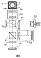
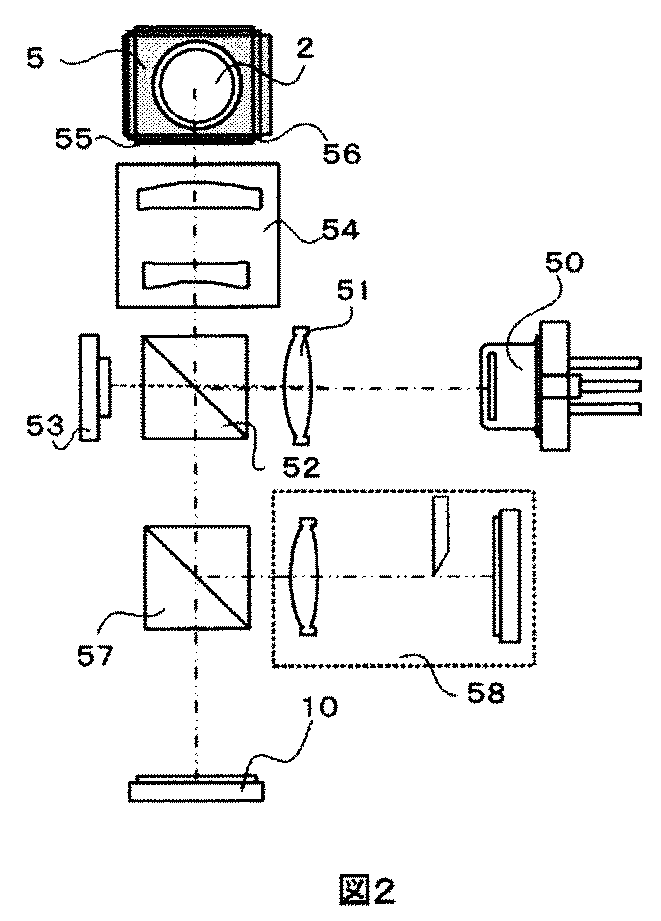
上記のような光ピックアップ装置において、図2は光学系について示している。ここではBDについて説明するが、HD DVDや他の記録方式であってもなんら構わない。 In the optical pickup device as described above, FIG. 2 shows an optical system. Here, BD will be described, but HD DVD or other recording methods may be used.
半導体レーザ50からは、波長略405nmの光束が発散光として出射される。半導体レーザ50から出射した光束はコリメートレンズ51により略平行な光束に変換される。コリメートレンズ51を透過した光束はビームスプリッタ52を反射する。なお一部の光束はビームスプリッタ52を透過しフロントモニタ53に入射する。一般的にBD−RE、BD−Rなどの記録型の光ディスクに情報を記録する場合には、光ディスクの記録面に所定の光量を照射させるため、半導体レーザの光量を高精度に制御する必要がある。このため、フロントモニタ53は記録型の光ディスクに信号を記録する際に、半導体レーザ50の光量の変化を検出し、半導体レーザ50の駆動回路(図示せず)にフィードバックされる。これにより光ディスク上の光量をモニタすることが可能となる。
From the
ビームスプリッタ52を反射した光束はビームエキスパンダ54に入射する。ビームエキスパンダ54は、光束の発散・収束状態を変えることで、光ディスク100のカバー層の厚み誤差による球面収差を補償することに使用される。ビームエキスパンダ54を出射した光束は立ち上げミラー55を反射、1/4波長板56を透過後、アクチュエータ5に搭載された対物レンズ2により光ディスク100上に集光される。
The light beam reflected by the
光ディスク100により反射した光束は、対物レンズ2、1/4波長板56、立ち上げミラー55、ビームエキスパンダ54、ビームスプリッタ52を透過する。ビームスプリッタ52を透過した光束はビームスプリッタ57を透過する光束と反射する光束に分岐される。
The light beam reflected by the
ビームスプリッタ57を反射した光束はナイフエッジ法によりフォーカス誤差信号が検出される。なお、ここではフォーカス検出方式にナイフエッジ法を用いているが、これに限定されるものではない。またナイフエッジ方式は公知であるため説明は省略する。ビームスプリッタ56を透過した光束は検出器10に入射する。この検出器10によりディスク上の信号およびトラッキング誤差信号を検出する。
A focus error signal is detected from the light beam reflected by the
図3は本発明の受光部パターンを示している。受光部10は、領域I(領域1)、領域J(領域2)、領域G(領域3)、領域H(領域4)の4領域を有し、領域I(領域1)および領域G(領域3)と領域J(領域2)および領域H(領域4)は受光部の中心線に対して線対称である。また、領域I(領域1)と領域J(領域2)は中心軸(または中心線)500から略垂直方向に離れるに従って中心軸500方向の幅が狭くなることを特徴としている。
FIG. 3 shows a light receiving portion pattern of the present invention. The
ここで、1ビーム方式のトラッキング誤差信号検出原理について図3で説明する。検出器面上ではディスクによって回折された0次回折光と±1次回折光とが干渉する領域が発生する。この領域の干渉の状態がトラック上のスポット位置によって異なるため、それを利用して所望のトラック位置にスポットを配置することができるのである。実際には、0次回折光、+1次回折光の干渉領域Z1で得られる信号と0次回折光、−1次回折光の干渉領域Z2で得られる信号の差を演算することでプッシュプル信号が生成される。また、この干渉領域以外はトラック上のスポット位置によってほとんど変化しない。1ビーム方式はこの特性を利用しているのである。 Here, the principle of detecting a tracking error signal of the one beam system will be described with reference to FIG. On the detector surface, an area where the 0th-order diffracted light diffracted by the disk and ± 1st-order diffracted light interfere is generated. Since the state of interference in this region differs depending on the spot position on the track, the spot can be arranged at a desired track position using this. In practice, a push-pull signal is generated by calculating the difference between the signal obtained in the interference region Z1 of the 0th-order diffracted light and the + 1st-order diffracted light and the signal obtained in the interference region Z2 of the 0th-order diffracted light and the −1st-order diffracted light. . Further, the area other than the interference area hardly changes depending on the spot position on the track. The 1-beam method uses this characteristic.
以下、詳細に説明していく。受光部上で光束は対物レンズの変位に伴い図3矢印の方向に変位する。それと同時に強度分布中心も同じ方向に変位する。この二つ影響により(I−J)の信号にDCオフセットが発生する。また(G−H)信号でもDCオフセットが発生する。図4は対物レンズ変位量に対する(I−J)の信号と(G−H)信号のオフセット量を示したものである。この図より、(I−J)の信号と(G−H)信号のオフセット量は対物レンズの変位に対してほぼ線形のDCオフセットが発生していることがわかる。そのため、以下の演算を行うとDCオフセットの抑制されたトラッキング誤差信号が検出できることがわかる。
This will be described in detail below. The light beam is displaced in the direction of the arrow in FIG. 3 with the displacement of the objective lens on the light receiving unit. At the same time, the intensity distribution center is displaced in the same direction. Due to these two effects, a DC offset occurs in the signal (I−J). In addition, a DC offset also occurs in the (GH) signal. FIG. 4 shows the offset amounts of the (I-J) signal and the (GH) signal with respect to the objective lens displacement amount. From this figure, it can be seen that the offset amount of the (I-J) signal and the (GH) signal has a substantially linear DC offset with respect to the displacement of the objective lens. Therefore, it can be seen that a tracking error signal with a suppressed DC offset can be detected by performing the following calculation.
ここでkは、(I−J)の信号にDCオフセットと(G−H)信号のDCオフセットを補正する係数である。このようにして1ビーム方式はオフセットを抑制したトラッキング誤差信号を検出可能となる。
Here, k is a coefficient for correcting the DC offset of the (I−J) signal and the DC offset of the (GH) signal. In this way, the one-beam method can detect a tracking error signal with suppressed offset.
次に、ディスク上の未記録領域と記録領域の境界部で発生するトラッキング誤差信号のオフセットについて説明する。図5は未記録領域と記録領域の境界での1ビーム方式のトラッキング誤差信号波形を模式的に示した図である。図5(1)はオフセットを抑制できない場合を示しており、図5(2)は過剰補正により逆側にオフセットが発生している場合を示している。そして、図5(3)はオフセットを抑制したトラッキング誤差信号である。 Next, the offset of the tracking error signal generated at the boundary between the unrecorded area and the recorded area on the disc will be described. FIG. 5 is a diagram schematically showing a tracking error signal waveform of the one-beam method at the boundary between the unrecorded area and the recorded area. FIG. 5 (1) shows a case where the offset cannot be suppressed, and FIG. 5 (2) shows a case where the offset occurs on the reverse side due to overcorrection. FIG. 5 (3) shows a tracking error signal in which the offset is suppressed.
図5(1)、図5(2)のようなトラッキング誤差信号波形では、ばらつき等によりトラッキング誤差信号が原点位置をクロスしなくなる可能性が大きくなる。もし、トラッキング誤差信号がクロスしないとサーボ制御上問題となる。(トラッキング制御は、この原点位置でサーボ制御を行う。)このため、図5(3)のような波形が望ましいことは明らかである。 In the tracking error signal waveforms as shown in FIGS. 5A and 5B, there is a high possibility that the tracking error signal does not cross the origin position due to variations or the like. If the tracking error signal does not cross, there will be a problem in servo control. (For tracking control, servo control is performed at this origin position.) For this reason, it is clear that a waveform as shown in FIG.
ここで、トラッキング誤差信号のオフセットの指標としてボトムの割合、トップの割合を考える。ボトムの割合とは図5に示す(a−c)/(c+d)とする。これは記録領域でのトラッキング誤差信号ボトム値と未記録領域と記録領域の境界でのトラッキング誤差信号ボトム値の差をとり、記録領域のトラッキング誤差信号振幅で割ったものであり、すなわち記録領域のトラッキング誤差信号振幅と比較した場合にどのくらいボトムが下側にあるかということを示している。
それに対し、トップの割合は(b−d)/(c+d)とする。これは記録領域でのトラッキング誤差信号トップの値と未記録領域と記録領域の境界でのトラッキング誤差信号トップの値の差をとり、記録領域のトラッキング誤差信号振幅で割ったものであり、すなわち記録領域のトラッキング誤差信号振幅と比較した場合にどのくらいトップが上側にあるかということを示している。
Here, the bottom ratio and the top ratio are considered as an index of the tracking error signal offset. The ratio of the bottom is (ac) / (c + d) shown in FIG. This is the difference between the bottom value of the tracking error signal in the recording area and the bottom value of the tracking error signal at the boundary between the unrecorded area and the recording area, and divided by the tracking error signal amplitude of the recording area. It shows how far the bottom is when compared to the tracking error signal amplitude.
On the other hand, the ratio of the top is (b−d) / (c + d). This is the difference between the tracking error signal top value in the recording area and the tracking error signal top value at the boundary between the unrecorded area and the recording area, and divided by the tracking error signal amplitude in the recording area. It shows how much the top is on the upper side when compared with the tracking error signal amplitude of the region.
この2つの指標がプラスの値であれば図5(3)のように未記録領域から記録領域にスポットが移動してもトラッキング誤差信号振幅が徐々に変化するため、サーボ制御が安定することがわかる。ところが2つの指標がプラスの値、マイナスの値の関係である場合、オフセットは抑制できていないため問題となる。
また、トラッキング誤差信号のオフセットは、対物レンズがトラッキング方向に変位した場合にもDCオフセットが発生する。このため、未記録領域、記録領域の境界と対物レンズ変位によるオフセットが同時に抑制される必要がある。
If these two indexes are positive values, the servo error can be stabilized because the tracking error signal amplitude gradually changes as the spot moves from the unrecorded area to the recorded area as shown in FIG. 5 (3). Recognize. However, if the two indexes have a relationship between a positive value and a negative value, there is a problem because the offset cannot be suppressed.
Further, the offset of the tracking error signal also occurs when the objective lens is displaced in the tracking direction. For this reason, the offset due to the unrecorded area, the boundary of the recorded area and the displacement of the objective lens needs to be suppressed simultaneously.
以下、このような指標を元に対物レンズが変位した場合の未記録領域、記録領域の境界部で発生するトラッキング誤差信号のオフセットの評価を行っていく。ここで、シミュレーション上の計算条件は以下の通りである。
波長:405nm
対物レンズNA:0.85
トラックピッチ:0.32μm
対物レンズ焦点距離:1.41mm
図6(1)は、本発明と特許文献1の受光部を用いて対物レンズがトラッキング方向に変位した時のトップの割合、図6(2)はボトムの割合を示したものである。本発明の受光部の条件として、検出器に入射する光束径に対する領域I(領域1)と領域J(領域2)の間隔の比率t1は、t1=d2/d1=0.19、検出器に入射する光束径に対する領域I(領域1)と領域J(領域2)の中心軸方向の最大幅の比率t2は、t2=d3/d1=0.5、領域I(領域1)と領域J(領域2)の中心軸に垂直な方向に対して領域の外形の傾き角度θは、θ=10degとした。
Hereinafter, based on such an index, the offset of the tracking error signal generated at the boundary between the unrecorded area and the recorded area when the objective lens is displaced is evaluated. Here, the calculation conditions in the simulation are as follows.
Wavelength: 405nm
Objective lens NA: 0.85
Track pitch: 0.32 μm
Objective lens focal length: 1.41 mm
FIG. 6A shows the ratio of the top when the objective lens is displaced in the tracking direction using the light receiving unit of the present invention and
図6より特許文献1は、トップの割合で大部分の対物レンズ変位量でマイナスの値となっている。そして、ボトムの割合はプラスの値になっており、オフセットが発生していることがわかる。
From FIG. 6,
それに対し、本発明のトップの割合、ボトムの割合は、対物レンズの変位量ほとんどの範囲でプラスとなり、未記録領域と記録領域の境界のオフセットを抑制できていることがわかる。 On the other hand, the ratio of the top and the ratio of the bottom of the present invention is positive in almost the range of displacement of the objective lens, and it can be seen that the offset of the boundary between the unrecorded area and the recorded area can be suppressed.
次に領域I、領域Jの分割線を傾けたことに対する効果について説明する。図7は傾けない場合と傾けた場合についてシミュレーションを行った結果で、図7(1)はトップの割合、図7(2)はボトムの割合を示している。なお、受光部の条件としては、t1=0.19、t2=0.5、θ=10degとt1=0.19、t2=0.5、θ=0degとしている。 Next, the effect of tilting the dividing lines of the region I and the region J will be described. FIGS. 7A and 7B show the results of simulation for the case of not tilting and the case of tilting. FIG. 7A shows the ratio of the top and FIG. 7B shows the ratio of the bottom. The conditions of the light receiving section are t1 = 0.19, t2 = 0.5, θ = 10 deg and t1 = 0.19, t2 = 0.5, and θ = 0 deg.
トップの割合では対物レンズの変位するほとんどの領域でプラスの値であり、また、ボトムの割合は対物レンズ変位がマイナスの領域で大きく改善している。このように、分割線を傾けた場合の方が未記録領域と記録領域の境界のオフセットを抑制することができる。特にθは、0度<θ<15度、t1、t2は、検出器10の受光部に入射する光束径に対して0<t1<0.35、0<t2<0.70の条件においてDCオフセットおよび未記録領域と記録領域の境界のオフセット抑制に大きな改善効果が得られる。
The ratio of the top is a positive value in most areas where the objective lens is displaced, and the ratio of the bottom is greatly improved in the area where the displacement of the objective lens is negative. As described above, when the dividing line is inclined, the offset of the boundary between the unrecorded area and the recorded area can be suppressed. In particular, θ is 0 ° <θ <15 °, and t1 and t2 are DC under the conditions of 0 <t1 <0.35 and 0 <t2 <0.70 with respect to the beam diameter incident on the light receiving portion of the
単純に考えると、図3のように領域Iと領域Jが中心軸500から略垂直方向に離れるに従って中心軸500方向の幅が狭くなれば、対物レンズが変位するのに対し、対物レンズが変位する方向の受光部領域(領域Iまたは領域J)の検出する干渉領域(干渉領域Z1または干渉領域Z2)の面積が減少するためトラッキング誤差信号振幅が極端に減少するように思われる。ところが、実際には、対物レンズが変位すると同時に、対物レンズ変位方向に対物レンズ変位量の2倍、光束の強度分布が変位する。このため、対物レンズが変位する方向の受光部領域(領域Iまたは領域J)上では、面積は小さくなるが強度が強くなる。また、対物レンズが変位する方向と逆の受光部領域(領域Jまたは領域I)上では、強度が弱くなるが面積が大きくなる。よってトラッキング誤差信号振幅が減少しにくく、DCオフセット補正もしやすい構成となっている。さらに、未記録領域と記録領域の境界のオフセットは、干渉領域(干渉領域Z1または干渉領域Z2)付近に顕著に発生するため、対物レンズの変位に対して干渉領域の外側をDCオフセット検出側の受光部に入射させるようにすることは未記録領域と記録領域の境界のオフセット抑制に効果的である。
Considering simply, if the width in the direction of the
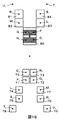
図3では検出器内側の分割線はトラックに対して略平行な直線と、そこから別の角度を持った直線で示したが図8の(1)ように受光部内側の分割線は弧であってもよいし、図8(2)のように直線であってもなんら問題ない。
また、ここでは受光部のパターンと示したが、図9の光学系のように受光部のパターンと同じパターンの回折格子101を配置して、それぞれの領域での回折方向、角度を変えて検出器上の複数の受光部で信号検出しても同様の効果があることは言うまでもない。
In FIG. 3, the dividing line inside the detector is shown as a straight line that is substantially parallel to the track and a straight line having a different angle from the straight line. However, as shown in FIG. There may be no problem even if it is a straight line as shown in FIG.
Although the light receiving portion pattern is shown here, the
図10は本発明の第2の実施例に係る実施例1と異なる受光部のパターンについて示している。実施例1との違いは中央領域Y(領域5)を設けていることを特徴としている。中央領域は、検出器10の受光部に入射する光束径に対して中央軸方向の長さの比率はt3、中央軸に垂直な方向の長さの比率はt4となっている。この受光部は以下の演算を行うとトラッキング誤差信号生成できる。
FIG. 10 shows a light receiving portion pattern different from that of the first embodiment according to the second embodiment of the present invention. A difference from the first embodiment is that a central region Y (region 5) is provided. In the central region, the ratio of the length in the central axis direction to the diameter of the light beam incident on the light receiving portion of the
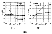
図11(1)は、本発明と特許文献1の受光部を用いて対物レンズがトラッキング方向に変位した時のトップの割合、図11(2)はボトムの割合を示したものである。本発明の受光部の条件としてはt1=0.19、t2=0.54、t3=0.19、t4=0.19、θ=10degとして計算を行った。
FIG. 11 (1) shows the ratio of the top when the objective lens is displaced in the tracking direction using the light receiving unit of the present invention and
図11より、特許文献1のトラッキング誤差信号は未記録領域と記録領域の境界の特性は対物レンズの変位に伴って大きく変化している。それに対し、本発明のトラッキング誤差信号は対物レンズ変位量に依らない。このため、レンズの変位に対し特別な制御は不要となる。また、対物レンズの変位量ほとんどの範囲でプラスとなり、未記録領域と記録領域の境界のオフセットを抑制できていることがわかる。
As shown in FIG. 11, in the tracking error signal of
これにより、本発明のような検出器パターンにすることで対物レンズが変位しても安定したトラッキング制御が行える。特にθは、0度<θ<15度、t1、t2、t3、t4は、検出器10の受光部に入射する光束径に対して0<t1、0.35、0<t2<0.70、0<t3<0.35、0<t4<0.35の条件においてDCオフセットおよび未記録領域と記録領域の境界のオフセット抑制に大きな改善効果が得られる。
Thus, by using the detector pattern as in the present invention, stable tracking control can be performed even if the objective lens is displaced. In particular, θ is 0 degree <θ <15 degrees, t1, t2, t3, and t4 are 0 <t1, 0.35, and 0 <t2 <0.70 with respect to the diameter of the light beam incident on the light receiving portion of the
実施例1でも述べたように未記録領域と記録領域の境界のオフセットは、干渉領域(干渉領域Z1または干渉領域Z2)付近に顕著に発生するため、検出面の中央部は影響しにくい。さらに、この領域をトラッキング誤差信号として検出しないことで係数kを適当な値にすることができるため、結果として未記録領域と記録領域の境界のオフセット抑制効果を向上することが可能となる。 As described in the first embodiment, the offset at the boundary between the unrecorded area and the recorded area is remarkably generated in the vicinity of the interference area (interference area Z1 or interference area Z2), so that the central portion of the detection surface is hardly affected. Further, the coefficient k can be set to an appropriate value by not detecting this area as a tracking error signal. As a result, the effect of suppressing the offset between the unrecorded area and the recorded area can be improved.
図10では検出器内側の分割線はトラックに対して略平行な直線と、そこから別の角度を持った直線で示したが図12の(1)ように受光部内側の分割線は弧であってもよいし、図12(2)のように直線であってもなんら問題ない。 In FIG. 10, the dividing line inside the detector is shown as a straight line substantially parallel to the track and a straight line having a different angle therefrom, but the dividing line inside the light receiving unit is an arc as shown in FIG. There may be no problem even if it is a straight line as shown in FIG.
また、ここでは受光部のパターンと示したが、実施例1のように受光部のパターンと同じパターンの回折格子101を配置して検出器上の複数の受光部で信号検出しても同様の効果があることは言うまでもない。
Although the light receiving unit pattern is shown here, the
図13は本発明の第3の実施例に係る光ピックアップ装置の光学系について示している。図2に示した本発明実施例1と同じ光学部品には同じ番号を付している。ここではBDについて説明するが、HD DVDや他の記録方式であってもなんら構わない。 FIG. 13 shows an optical system of an optical pickup device according to the third embodiment of the present invention. The same optical parts as those of the first embodiment shown in FIG. Here, BD will be described, but HD DVD or other recording methods may be used.
半導体レーザ50からは、波長略405nmの光束が発散光として出射される。半導体レーザ50から出射した光束はビームスプリッタ52を反射する。なお一部の光束はビームスプリッタ52を透過しフロントモニタ53に入射する。ビームスプリッタ52を反射した光束はコリメートレンズ51により略平行な光束に変換される。コリメートレンズ51を透過した光束はビームエキスパンダ54に入射する。ビームエキスパンダ54を出射した光束は立ち上げミラー55を反射、1/4波長板56を透過後、アクチュエータ5に搭載された対物レンズ2により光ディスク100上に集光される。
From the
光ディスク100により反射した光束は、対物レンズ2、1/4波長板56、立ち上げミラー55、ビームエキスパンダ54、コリメートレンズ51、ビームスプリッタ52を透過する。
The light beam reflected by the
ビームスプリッタ52を透過した光束は、回折格子11により、フォーカス誤差信号(0次回折光)を生成する光束とトラッキング誤差信号(+1次回折光または−1次光)を生成する光束とに分岐される。ここでは、実施例1の図3の回折格子で説明を行うが、実施例1の図8(1)または図8(2)または実施例2の図10または図12(1)または図12(2)の回折格子であっても問題ない。
回折格子11によって分岐された光束は検出レンズに入射する。検出レンズでは、光束が透過するときに所定の非点収差が与えられ、フォーカス誤差信号検出に用いられる。また、トラッキング誤差信号を生成する光束は回折格子11を回折するときに非点収差、球面収差を与えられているため、検出レンズ59を透過した光束は受光部上に集光する。
The light beam that has passed through the
The light beam branched by the
図14は、検出器12と検出される光束を示したものである。検出器12はフォーカス検出用の領域40〜43とトラッキング誤差信号領域44〜47とに分けられる。フォーカス誤差信号に関しては公知であるため、説明は省略する。回折格子11を回折した光束は、ぞれぞれの領域で回折方向が異なるため図1の領域Gを回折した光束が図14の領域45、領域Hを回折した光束が領域46、領域Iを回折した光束が領域44、領域Jを回折した光束が領域47にそれぞれ入射する。これによりトラッキング誤差信号が生成される。ここではRF信号はフォーカス誤差信号の和またはトラッキング誤差信号の和またはフォーカス誤差信号とトラッキング誤差信号の和をとることで検出可能である。また、DVD−ROM等で採用されているトラッキング誤差信号検出方式のDPD(Differential Phase Ditection)についてもフォーカス誤差用の領域40〜43の検出信号を用いれば対応可能である。
FIG. 14 shows the
このような光学系構成とすることでトラッキング誤差信号だけでなく他の信号も得ることが可能となる。ここでは回折格子11を検出側に配置したが、図15のように偏光性回折格子13を用いて対物レンズに近いところに配置しても問題ない。
With such an optical system configuration, not only the tracking error signal but also other signals can be obtained. Although the
図16は本発明の第4の実施例に係る光ピックアップ装置の光学系について示している。図2に示した本発明実施例1と同じ光学部品には同じ番号を付している。ここではBDについて説明するが、HD DVDや他の記録方式であってもなんら構わない。 FIG. 16 shows an optical system of an optical pickup device according to the fourth embodiment of the present invention. The same optical parts as those of the first embodiment shown in FIG. Here, BD will be described, but HD DVD or other recording methods may be used.
半導体レーザ90からは、波長略405nmの光束が発散光としてP偏光の光束が出射される。半導体レーザ90から出射した光束はビームスプリッタ91を透過し、ミラー92を反射する。なお有効径外の一部の光束はフロントモニタ93に入射する。ミラー92を反射した光束は補助レンズ94、コリメートレンズ95に入射する。コリメートレンズ95は駆動装置(図示せず)により、光軸の方向に駆動可能となっているため、光束の発散・収束状態を変えることで、光ディスク100のカバー層の厚み誤差による球面収差を補償することができる。
The
コリメートレンズ95を透過したP偏光の光束は本発明の偏光性回折格子14に入射する。偏光性回折格子14に入射したP偏光の光束はそのまま透過し、立ち上げミラー96を反射、1/4波長板97を透過後、円偏光となる。円偏光となった光束がアクチュエータ5に搭載された対物レンズ2により光ディスク100上に集光される。
The P-polarized light beam transmitted through the collimating
光ディスク100により反射した光束は、対物レンズ2、1/4波長板97を透過する。円偏光の光束は1/4波長板97によりS偏光となる。S偏光の光束は立ち上げミラー96を反射し、偏光性回折格子14に入射する。入射したS偏光は、偏光性回折格子14により複数の光束に分けられる。偏光性回折格子14を透過した光束はコリメートレンズ95、補助レンズ94、ミラー92を経てビームスプリッタ91を反射し、検出器15に入射する。
The light beam reflected by the
図17、図18はトラッキング誤差信号だけでなくフォーカス誤差信号まで考慮した偏光性回折格子14のパターン(図17)、検出器15(図18)を示している。偏光性回折格子14は±1次光のみが回折される回折格子であり、回折した光束は、ぞれぞれの領域で回折方向および回折角が異なる。簡単のため、図18では、図17で示す偏光性回折格子のそれぞれの領域から回折した光束を領域の文字で示している。また、その文字の下付きの文字は+ならば+1次回折光、−ならば−1次回折光を示している。例えば図17偏光性回折格子14の領域Lの+1次回折光は、図18検出器21の領域74に入射、ー1次回折光は、領域83に入射する。
FIGS. 17 and 18 show the pattern of the polarizing diffraction grating 14 (FIG. 17) and the detector 15 (FIG. 18) considering not only the tracking error signal but also the focus error signal. The
フォーカス誤差信号検出方式はナイフエッジ方式であり、偏光回折格子17の領域N、P、Q、Oにより回折したー1次回折光で検出する。ナイフエッジ方式は公知であるため、説明は省略する。トラッキング誤差信号検出は領域70〜79、領域81〜84の検出信号を用いて以下の演算を行うことで得られる。
The focus error signal detection method is a knife edge method, and detection is performed using first-order diffracted light diffracted by the regions N, P, Q, and O of the polarization diffraction grating 17. Since the knife edge method is well-known, description is abbreviate | omitted. The tracking error signal detection is obtained by performing the following calculation using the detection signals in the
偏光性回折格子14はフォーカス検出等のために複数の領域に分割されているが、トラッキング誤差信号の観点から言えば実施例2の図10と同様の検出方式である。
さらにRF信号検出は、領域70〜79の検出信号を用いて以下の演算を行うことで得られる。
The
Further, the RF signal detection can be obtained by performing the following calculation using the detection signals in the
またDPD信号検出は、領域70〜77の検出信号を用いて以下の演算を行うことで得られる。
The DPD signal detection is obtained by performing the following calculation using the detection signals in the
このような光学系構成とすることでトラッキング誤差信号だけでなく他の信号も得ることが可能となる。
With such an optical system configuration, not only the tracking error signal but also other signals can be obtained.
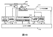
実施例5では、光ピックアップ装置1を搭載した、光学的再生装置について説明する。図19は光学的再生装置の概略構成である。光ピックアップ装置1は、光ディスク100の半径方向に沿って駆動できる機構が設けられており、アクセス制御回路172からのアクセス制御信号に応じて位置制御される。
In Example 5, an optical reproducing apparatus equipped with the
レーザ点灯回路177からは所定のレーザ駆動電流が光ピックアップ装置1内の半導体レーザに供給され、半導体レーザからは再生に応じて所定の光量でレーザ光が出射される。なお、レーザ点灯回路177は光ピックアップ装置1内に組み込むこともできる。
A predetermined laser driving current is supplied from the
光ピックアップ装置1内の光検出器から出力された信号は、サーボ信号生成回路174および情報信号再生回路175に送られる。サーボ信号生成回路174では前記光検出器からの信号に基いてフォーカス誤差信号、トラッキング誤差信号ならびにチルト制御信号などのサーボ信号が生成され、これを基にアクチュエータ駆動回路173を経て光ピックアップ装置1内のアクチュエータを駆動して、対物レンズの位置制御がなされる。
The signal output from the photodetector in the
前記情報信号再生回路175では、前記光検出器からの信号に基づいて光ディスク100に記録されている情報信号が再生される。
前記サーボ信号生成回路174および情報信号再生回路175で得られた信号の一部はコントロール回路176に送られる。このコントロール回路176にはスピンドルモータ駆動回路171、アクセス制御回路172、サーボ信号生成回路174、レーザ点灯回路177、球面収差補正素子駆動回路179などが接続され、光ディスク100を回転させるスピンドルモータ180の回転制御、アクセス方向およびアクセス位置の制御、対物レンズのサーボ制御、光ピックアップ装置1内の半導体レーザ発光光量の制御、ディスク基板厚さの違いによる球面収差の補正などが行われる。
The information
Part of the signals obtained by the servo
実施例6では、光ピックアップ装置1を搭載した、光学的記録再生装置について説明する。図20は光学的記録再生装置の概略構成である。この装置で前記図19に説明した光学的情報記録再生装置と相違する点は、コントロール回路176とレーザ点灯回路177の間に情報信号記録回路178を設け、情報信号記録回路178からの記録制御信号に基づいてレーザ点灯回路177の点灯制御を行って、光ディスク100へ所望の情報を書き込む機能が付加されている点である。
In Example 6, an optical recording / reproducing apparatus equipped with the
1:光ピックアップ装置、2:対物レンズ、5:アクチュエータ、7:駆動機構、10:検出器、11:回折格子、12:検出器、13:回折格子、14:回折格子、15、検出器、19:検出器、40〜47:受光部の領域、50:半導体レーザ、51:コリメートレンズ、52:ビームスプリッタ、53:フロントモニタ、54:ビームエキスパンダ、55:立ち上げミラー、70〜84:受光部の領域、101:回折格子、56:1/4波長板、57:ビームスプリッタ、58:フォーカス検出器、59:検出レンズ、
90:半導体レーザ、91:ビームスプリッタ、92:ミラー、93:フロントモニタ、94:補助レンズ、95:コリメートレンズ、96:立ち上げミラー、97:1/4波長板、171:スピンドルモータ、172:アクセス制御、173:アクチュエータ駆動回路、174:サーボ信号生成回路、175:情報信号再生回路、176:コントロール回路、177:レーザ点灯回路、178:情報記録回路、179:球面収差補正素子駆動回路、180:スピンドルモータ、500:回折格子中心軸
1: optical pickup device, 2: objective lens, 5: actuator, 7: drive mechanism, 10: detector, 11: diffraction grating, 12: detector, 13: diffraction grating, 14: diffraction grating, 15, detector, 19: detector, 40 to 47: light receiving area, 50: semiconductor laser, 51: collimating lens, 52: beam splitter, 53: front monitor, 54: beam expander, 55: rising mirror, 70 to 84: Region of light receiving unit, 101: diffraction grating, 56: 1/4 wavelength plate, 57: beam splitter, 58: focus detector, 59: detection lens,
90: Semiconductor laser, 91: Beam splitter, 92: Mirror, 93: Front monitor, 94: Auxiliary lens, 95: Collimating lens, 96: Raising mirror, 97: 1/4 wavelength plate, 171: Spindle motor, 172: Access control, 173: Actuator drive circuit, 174: Servo signal generation circuit, 175: Information signal reproduction circuit, 176: Control circuit, 177: Laser lighting circuit, 178: Information recording circuit, 179: Spherical aberration correction element drive circuit, 180 : Spindle motor, 500: Diffraction grating center axis
Claims (8)
前記半導体レーザから出射された光束を光ディスクに照射する対物レンズと、
光ディスクから反射した光束を受光する光検出器と、
を備えた光ピックアップ装置であって、
前記光検出器は、領域1、領域2、領域3、領域4の4領域を有する受光部があり、
前記受光部の領域1および領域3と領域2および領域4は前記受光部の中心線に対して線対称であり、
前記受光部の領域1と領域2は前記中心線から離れるにしたがって幅が狭くなり、
前記受光部の領域1、領域2、領域3、領域4で検出される信号を出力する、
光ピックアップ装置。 A semiconductor laser that emits laser light;
An objective lens for irradiating an optical disk with a light beam emitted from the semiconductor laser;
A photodetector for receiving the light beam reflected from the optical disc;
An optical pickup device comprising:
The photodetector has a light receiving unit having four regions of region 1, region 2, region 3, and region 4,
Regions 1 and 3 and regions 2 and 4 of the light receiving portion are line symmetric with respect to the center line of the light receiving portion,
The area 1 and the area 2 of the light receiving portion become narrower as they move away from the center line,
Outputting signals detected in the area 1, area 2, area 3, and area 4 of the light receiving unit;
Optical pickup device.
前記半導体レーザから出射された光束を光ディスクに照射する対物レンズと、
光ディスクから反射した光束を分岐する回折格子と、
前記回折格子により分岐された光束を受光する光検出器と、
を備えた光ピックアップ装置であって、
前記回折格子は、領域1、領域2、領域3、領域4の4領域を有しており、
前記回折格子の領域1および領域3と領域2および領域4は前記回折格子の中心線に対して線対称であり、
前記回折格子の領域1と領域2は前記中心線から離れるにしたがって幅が狭くなり、
前記回折格子の領域1、領域2、領域3、領域4の回折光から検出される信号を出力する、
光ピックアップ装置。 A semiconductor laser that emits laser light;
An objective lens for irradiating an optical disk with a light beam emitted from the semiconductor laser;
A diffraction grating for branching the light beam reflected from the optical disc;
A photodetector for receiving a light beam branched by the diffraction grating;
An optical pickup device comprising:
The diffraction grating has four regions of region 1, region 2, region 3, and region 4,
Regions 1 and 3 and regions 2 and 4 of the diffraction grating are line symmetric with respect to the center line of the diffraction grating,
Regions 1 and 2 of the diffraction grating become narrower with distance from the center line,
Outputting a signal detected from the diffracted light of region 1, region 2, region 3 and region 4 of the diffraction grating;
Optical pickup device.
前記半導体レーザから出射された光束を光ディスクに照射する対物レンズと、
光ディスクから反射した光束を受光する光検出器と、
を備えた光ピックアップ装置であって、
前記光検出器は、領域1、領域2、領域3、領域4、領域5の5領域を有する受光部があり、
前記受光部の領域1および領域3と領域2および領域4は前記受光部の中心線に対して線対称であり、
前記受光部の領域5は、前記中心線に対して線対称かつ前記中心線上に形成されており、
前記受光部の領域1と領域2は前記中心線から離れるにしたがって幅が狭くなり、
前記受光部の領域1、領域2、領域3、領域4で検出される信号を出力する、
光ピックアップ装置。 A semiconductor laser that emits laser light;
An objective lens for irradiating an optical disk with a light beam emitted from the semiconductor laser;
A photodetector for receiving the light beam reflected from the optical disc;
An optical pickup device comprising:
The photodetector has a light receiving section having five areas of area 1, area 2, area 3, area 4, and area 5,
Regions 1 and 3 and regions 2 and 4 of the light receiving portion are line symmetric with respect to the center line of the light receiving portion,
The region 5 of the light receiving part is formed symmetrically with respect to the center line and on the center line.
The area 1 and the area 2 of the light receiving portion become narrower as they move away from the center line,
Outputting signals detected in the area 1, area 2, area 3, and area 4 of the light receiving unit;
Optical pickup device.
前記半導体レーザから出射された光束を光ディスクに照射する対物レンズと、
光ディスクから反射した光束を分岐する回折格子と、
前記回折格子により分岐された光束を受光する光検出器と、
を備えた光ピックアップ装置であって、
前記回折格子は、領域1、領域2、領域3、領域4、領域5の5領域を有しており、
前記回折格子の領域1および領域3と領域2および領域4は前記回折格子の中心線に対して線対称であり、
前記回折格子の領域5は、前記中心線に対して線対称かつ前記中心線上に形成されており、
前記回折格子の領域1と領域2は前記中心線から離れるにしたがって幅が狭くなり、
前記回折格子の領域1、領域2、領域3、領域4の回折光から検出される信号を出力する、
光ピックアップ装置。 A semiconductor laser that emits laser light;
An objective lens for irradiating an optical disk with a light beam emitted from the semiconductor laser;
A diffraction grating for branching the light beam reflected from the optical disc;
A photodetector for receiving a light beam branched by the diffraction grating;
An optical pickup device comprising:
The diffraction grating has five regions of region 1, region 2, region 3, region 4, and region 5,
Regions 1 and 3 and regions 2 and 4 of the diffraction grating are line symmetric with respect to the center line of the diffraction grating,
The region 5 of the diffraction grating is formed in line symmetry with respect to the center line and on the center line,
Regions 1 and 2 of the diffraction grating become narrower with distance from the center line,
Outputting a signal detected from the diffracted light of region 1, region 2, region 3 and region 4 of the diffraction grating;
Optical pickup device.
前記半導体レーザから出射された光束を光ディスクに照射する対物レンズと、
光ディスクから反射した光束を受光する光検出器と、
を備えた光ピックアップ装置であって、
前記光検出器は、領域1、領域2、領域3、領域4、領域5、領域6、領域7を有する受光部があり、
前記受光部の領域1および領域3および領域6と領域2および領域4および領域7は前記受光部の中心線に対して線対称であり、
前記受光部の領域5は、さらに領域8、領域9、領域10、領域11の4つの領域に細分されており、領域8および領域10と領域9および領域11は前記中心線に対して線対称に形成されており、
前記受光部の領域1と領域2は前記中心線から離れるにしたがって幅が狭くなり、かつ、領域1と領域2はさらに前記中心線と垂直な方向で2分されており、
前記受光部の領域1、領域2、領域3、領域4、領域5、領域6、領域7で検出される信号を出力する、
光ピックアップ装置。 A semiconductor laser that emits laser light;
An objective lens for irradiating an optical disk with a light beam emitted from the semiconductor laser;
A photodetector for receiving the light beam reflected from the optical disc;
An optical pickup device comprising:
The photodetector has a light receiving section having a region 1, a region 2, a region 3, a region 4, a region 5, a region 6, and a region 7.
Region 1 and region 3 and region 6 and region 2 and region 4 and region 7 of the light receiving unit are line symmetric with respect to the center line of the light receiving unit,
The region 5 of the light receiving section is further subdivided into four regions of region 8, region 9, region 10 and region 11, and the regions 8 and 10 and regions 9 and 11 are line symmetric with respect to the center line. Is formed,
The region 1 and the region 2 of the light receiving portion become narrower as they move away from the center line, and the region 1 and the region 2 are further divided into two in a direction perpendicular to the center line,
Outputting signals detected in region 1, region 2, region 3, region 4, region 5, region 6, and region 7 of the light receiving unit;
Optical pickup device.
前記半導体レーザから出射された光束を光ディスクに照射する対物レンズと、
光ディスクから反射した光束を分岐する回折格子と、
前記回折格子により分岐された光束を受光する光検出器と、
を備えた光ピックアップ装置であって、
前記回折格子は、領域1、領域2、領域3、領域4、領域5、領域6、領域7を有しており、
前記回折格子の領域1および領域3および領域6と領域2および領域4および領域7は前記回折格子の中心線に対して線対称であり、
前記回折格子の領域5は、さらに領域8、領域9、領域10、領域11の4つの領域に細分されており、領域8および領域10と領域9および領域11は前記中心線に対して線対称に形成されており、
前記回折格子の領域1と領域2は前記中心線から離れるにしたがって幅が狭くなり、かつ、領域1と領域2はさらに前記中心線と垂直な方向で2分されており、
前記回折格子の領域1、領域2、領域3、領域4、領域5、領域6、領域7の回折光から検出される信号を出力する、
光ピックアップ装置。 A semiconductor laser that emits laser light;
An objective lens for irradiating an optical disk with a light beam emitted from the semiconductor laser;
A diffraction grating for branching the light beam reflected from the optical disc;
A photodetector for receiving a light beam branched by the diffraction grating;
An optical pickup device comprising:
The diffraction grating has a region 1, a region 2, a region 3, a region 4, a region 5, a region 6, and a region 7.
Region 1 and region 3 and region 6 and region 2 and region 4 and region 7 of the diffraction grating are line-symmetric with respect to the center line of the diffraction grating,
The region 5 of the diffraction grating is further subdivided into four regions of region 8, region 9, region 10, and region 11, and the regions 8, 10 and 9 and 11 are symmetrical with respect to the center line. Is formed,
Regions 1 and 2 of the diffraction grating become narrower as they move away from the center line, and regions 1 and 2 are further divided into two in a direction perpendicular to the center line,
Outputting a signal detected from the diffracted light of region 1, region 2, region 3, region 4, region 5, region 6, and region 7 of the diffraction grating;
Optical pickup device.
前記領域1と領域2は、前記中心線に垂直な方向に対して領域の外形が傾き角度θの辺を有し、
前記傾き角度θは0度<θ<15度である、
光ピックアップ装置。 The optical pickup device according to any one of claims 1 to 6,
The region 1 and the region 2 have sides having an inclination angle θ with respect to a direction perpendicular to the center line,
The tilt angle θ is 0 degree <θ <15 degrees.
Optical pickup device.
前記光ピックアップ装置から出力される信号を用いてトラッキング誤差信号を生成するサーボ信号生成回路と、
を有する光ディスク装置であって、
前記サーボ信号生成回路は、
前記領域1に入射し、前記検出器によって検出された信号A1と、
前記領域2に入射し、前記検出器によって検出された信号A2と、
前記領域3に入射し、前記検出器によって検出された信号A3と、
前記領域4に入射し、前記検出器によって検出された信号A4と、
前記領域1、領域2と領域3、領域4の光量を補正する係数kにより、
式(A1−A2)−k×(A3−A4)でトラッキング誤差信号を生成する、
光ディスク装置。
An optical pickup device according to any one of claims 1 to 6,
A servo signal generation circuit that generates a tracking error signal using a signal output from the optical pickup device;
An optical disc device having
The servo signal generation circuit includes:
A signal A1 incident on the region 1 and detected by the detector;
A signal A2 incident on the region 2 and detected by the detector;
A signal A3 incident on the region 3 and detected by the detector;
A signal A4 incident on the region 4 and detected by the detector;
By the coefficient k for correcting the light quantity of the region 1, the region 2, the region 3, and the region 4,
A tracking error signal is generated by Expression (A1-A2) -k × (A3-A4).
Optical disk device.
Priority Applications (9)
| Application Number | Priority Date | Filing Date | Title |
|---|---|---|---|
| JP2006283245A JP4719660B2 (en) | 2006-10-18 | 2006-10-18 | Optical pickup device and optical disk device |
| US11/680,705 US7567495B2 (en) | 2006-10-18 | 2007-03-01 | Optical pickup apparatus and optical disc apparatus using same |
| CN200710091083XA CN101165790B (en) | 2006-10-18 | 2007-04-06 | Optical pickup device and optical disc device having the same |
| CN201010167450A CN101853674A (en) | 2006-10-18 | 2007-04-06 | Optical pickup device and optical disc device having same |
| US11/979,130 US7940630B2 (en) | 2006-10-18 | 2007-10-31 | Optical pick up apparatus with a single beam system and having a diffraction grating |
| US11/979,129 US7885166B2 (en) | 2006-10-18 | 2007-10-31 | Optical pick up apparatus with a single beam system and having a diffraction grating |
| US11/979,131 US20080094976A1 (en) | 2006-10-18 | 2007-10-31 | Optical pickup apparatus and optical disc apparatus using same |
| US11/979,132 US20080093569A1 (en) | 2006-10-18 | 2007-10-31 | Optical pickup apparatus and optical disc apparatus using same |
| US12/497,966 US7978587B2 (en) | 2006-10-18 | 2009-07-06 | Optical pickup apparatus and optical disc apparatus with a single beam system |
Applications Claiming Priority (1)
| Application Number | Priority Date | Filing Date | Title |
|---|---|---|---|
| JP2006283245A JP4719660B2 (en) | 2006-10-18 | 2006-10-18 | Optical pickup device and optical disk device |
Publications (2)
| Publication Number | Publication Date |
|---|---|
| JP2008102995A true JP2008102995A (en) | 2008-05-01 |
| JP4719660B2 JP4719660B2 (en) | 2011-07-06 |
Family
ID=39437217
Family Applications (1)
| Application Number | Title | Priority Date | Filing Date |
|---|---|---|---|
| JP2006283245A Expired - Fee Related JP4719660B2 (en) | 2006-10-18 | 2006-10-18 | Optical pickup device and optical disk device |
Country Status (1)
| Country | Link |
|---|---|
| JP (1) | JP4719660B2 (en) |
Citations (1)
| Publication number | Priority date | Publication date | Assignee | Title |
|---|---|---|---|---|
| JPH04119531A (en) * | 1990-09-10 | 1992-04-21 | Mitsubishi Electric Corp | Optical pickup device |
-
2006
- 2006-10-18 JP JP2006283245A patent/JP4719660B2/en not_active Expired - Fee Related
Patent Citations (1)
| Publication number | Priority date | Publication date | Assignee | Title |
|---|---|---|---|---|
| JPH04119531A (en) * | 1990-09-10 | 1992-04-21 | Mitsubishi Electric Corp | Optical pickup device |
Also Published As
| Publication number | Publication date |
|---|---|
| JP4719660B2 (en) | 2011-07-06 |
Similar Documents
| Publication | Publication Date | Title |
|---|---|---|
| US7558170B2 (en) | Optical pick-up head, optical information apparatus, and optical information reproducing method | |
| US7885166B2 (en) | Optical pick up apparatus with a single beam system and having a diffraction grating | |
| CN101165790B (en) | Optical pickup device and optical disc device having the same | |
| JP4951538B2 (en) | Optical pickup device and optical disk device | |
| JP5002445B2 (en) | Optical pickup device and optical disk device | |
| US7800986B2 (en) | Optical pickup and optical disc apparatus | |
| JP2010033641A (en) | Optical pickup device, optical disk device and diffraction grating | |
| JP2005302253A (en) | Optical pickup apparatus having optical detection area for compensating tracking error offset | |
| JP4729418B2 (en) | Diffraction grating, optical pickup device, optical disk device | |
| JP4719660B2 (en) | Optical pickup device and optical disk device | |
| JP2009009628A (en) | Optical pickup and optical information reproducing apparatus | |
| JP4268971B2 (en) | Optical pickup | |
| JP5277207B2 (en) | Optical pickup device and optical disk device | |
| KR100692574B1 (en) | Diffraction element and optical pickup device comprising same | |
| JP2011187116A (en) | Optical pickup device and optical disk device | |
| JP2007234120A (en) | Optical pickup device and optical disk device | |
| JP2011248957A (en) | Optical pickup device, optical disk apparatus and photodetector | |
| JP2012133852A (en) | Optical pickup | |
| JP2009043306A (en) | Optical pickup and optical disc apparatus | |
| JP2013012276A (en) | Optical pickup device and optical disc apparatus equipped with the same | |
| JP2002312966A (en) | Optical pickup device |
Legal Events
| Date | Code | Title | Description |
|---|---|---|---|
| A621 | Written request for application examination |
Free format text: JAPANESE INTERMEDIATE CODE: A621 Effective date: 20090130 |
|
| A521 | Written amendment |
Free format text: JAPANESE INTERMEDIATE CODE: A523 Effective date: 20090130 |
|
| A977 | Report on retrieval |
Free format text: JAPANESE INTERMEDIATE CODE: A971007 Effective date: 20100812 |
|
| A131 | Notification of reasons for refusal |
Free format text: JAPANESE INTERMEDIATE CODE: A131 Effective date: 20100817 |
|
| A521 | Written amendment |
Free format text: JAPANESE INTERMEDIATE CODE: A523 Effective date: 20101015 |
|
| A521 | Written amendment |
Free format text: JAPANESE INTERMEDIATE CODE: A523 Effective date: 20101015 |
|
| A131 | Notification of reasons for refusal |
Free format text: JAPANESE INTERMEDIATE CODE: A131 Effective date: 20101130 |
|
| A521 | Written amendment |
Free format text: JAPANESE INTERMEDIATE CODE: A523 Effective date: 20110128 |
|
| A521 | Written amendment |
Free format text: JAPANESE INTERMEDIATE CODE: A523 Effective date: 20110128 |
|
| TRDD | Decision of grant or rejection written | ||
| A01 | Written decision to grant a patent or to grant a registration (utility model) |
Free format text: JAPANESE INTERMEDIATE CODE: A01 Effective date: 20110308 |
|
| A61 | First payment of annual fees (during grant procedure) |
Free format text: JAPANESE INTERMEDIATE CODE: A61 Effective date: 20110404 |
|
| R150 | Certificate of patent or registration of utility model |
Ref document number: 4719660 Country of ref document: JP Free format text: JAPANESE INTERMEDIATE CODE: R150 Free format text: JAPANESE INTERMEDIATE CODE: R150 |
|
| FPAY | Renewal fee payment (event date is renewal date of database) |
Free format text: PAYMENT UNTIL: 20140408 Year of fee payment: 3 |
|
| S531 | Written request for registration of change of domicile |
Free format text: JAPANESE INTERMEDIATE CODE: R313531 |
|
| R350 | Written notification of registration of transfer |
Free format text: JAPANESE INTERMEDIATE CODE: R350 |
|
| LAPS | Cancellation because of no payment of annual fees |