JP2008123738A - Optical device, method of manufacturing optical device, and electronic apparatus. - Google Patents
Optical device, method of manufacturing optical device, and electronic apparatus. Download PDFInfo
- Publication number
- JP2008123738A JP2008123738A JP2006303652A JP2006303652A JP2008123738A JP 2008123738 A JP2008123738 A JP 2008123738A JP 2006303652 A JP2006303652 A JP 2006303652A JP 2006303652 A JP2006303652 A JP 2006303652A JP 2008123738 A JP2008123738 A JP 2008123738A
- Authority
- JP
- Japan
- Prior art keywords
- layer
- inorganic
- optical device
- partition
- substrate
- Prior art date
- Legal status (The legal status is an assumption and is not a legal conclusion. Google has not performed a legal analysis and makes no representation as to the accuracy of the status listed.)
- Withdrawn
Links
Images


Landscapes
- Devices For Indicating Variable Information By Combining Individual Elements (AREA)
- Electroluminescent Light Sources (AREA)
Abstract
【課題】貫通孔に充填する液体材料の濡れ広がり方を均一化する。
【解決手段】基板10の上に、画素開口部50R,50G,50Bを画定する隔壁層13を形成する。次に、隔壁層13の表面に、隔壁層13の領域13rを覆う無機層14rを形成するとともに、無機層14rよりも厚みが薄い無機層であって、隔壁層13の領域13gを覆う無機層14gを形成する。次に、隔壁層13および無機層14r,14gが形成された基板10に対してフッ素プラズマ処理を施すことにより無機層14r,14gを除去するとともに、各領域13r,13g,13bを撥水化する。無機層14の有無および厚みを異ならせることにより、各領域13r,13g,13bの撥水性を相違させる。
【選択図】図1An object of the present invention is to uniformize the way in which a liquid material filling a through hole is spread.
A partition layer 13 is formed on a substrate 10 to define pixel openings 50R, 50G, and 50B. Next, an inorganic layer 14r that covers the region 13r of the partition layer 13 is formed on the surface of the partition layer 13, and is an inorganic layer that is thinner than the inorganic layer 14r and covers the region 13g of the partition layer 13 14 g is formed. Next, the substrate 10 on which the partition layer 13 and the inorganic layers 14r and 14g are formed is subjected to fluorine plasma treatment to remove the inorganic layers 14r and 14g and to make the regions 13r, 13g, and 13b water repellent. . The water repellency of each of the regions 13r, 13g, and 13b is made different by changing the presence / absence and thickness of the inorganic layer 14.
[Selection] Figure 1
Description
本発明は、複数の領域からの光をそれぞれ射出する光学装置およびその製造方法に関する。 The present invention relates to an optical device that emits light from a plurality of regions and a method for manufacturing the same.
光学装置として、例えば、複数種類の有機EL材料溶液を塗り分けて製造されるカラー有機EL(Electroluminescence)パネルがある。このカラー有機ELパネルの製造工程では、バンク(隔壁層)を形成することにより、複数の発光領域(貫通孔)が画定されることがある。各領域には、RGB各色用の有機EL材料溶液が充填される。このカラー有機ELパネルは、画像表示装置として用いられる。
このような光学装置の製造方法として、特許文献1には、その図23に示す方法が開示されている。この図23においては、バンク302の上面に一様に撥水処理を施すことにより撥水性の表面305を形成し、バンク302を挟んで隣接する凹部(発光領域)に、RGB各色用の有機EL材料溶液を充填する例が示されている。
As a method for manufacturing such an optical device,
ところで、上述した光学装置の製造方法では、有機EL材料溶液の濡れ広がり方が、その種類に応じて相違してしまう。この相違は、例えば、複数の発光領域間での輝度のばらつきを招く。
本発明は、上述した事情に鑑みてなされたものであり、異なる種類の液体がそれぞれ充填される複数の貫通孔間で液体の濡れ広がり方を均一とすることができる光学装置およびその製造方法を提供することを解決課題とする。
By the way, in the manufacturing method of the optical device described above, the way in which the organic EL material solution wets and spreads differs depending on the type. This difference causes, for example, variations in luminance among a plurality of light emitting regions.
The present invention has been made in view of the above-described circumstances, and provides an optical device and a method for manufacturing the same that can uniformly spread the liquid between a plurality of through holes filled with different types of liquids. Providing is a solution issue.
本発明に係る光学装置の製造方法は、基板の上に、有機材料で、複数の貫通孔(画素開口部、画素形成領域)を確定する隔壁層を形成する第1工程と、前記隔壁層の上に、無機材料で、前記隔壁層の上面の一部を覆う無機層を形成する第2工程と、前記隔壁層および前記無機層が形成された前記基板に対してフッ素プラズマ処理を施すことにより前記無機層を除去する第3工程とを有する。 The method for manufacturing an optical device according to the present invention includes a first step of forming a partition layer for defining a plurality of through holes (pixel openings, pixel formation regions) on a substrate with an organic material, A second step of forming an inorganic layer covering an upper surface of the partition wall layer with an inorganic material; and applying a fluorine plasma treatment to the substrate on which the partition layer and the inorganic layer are formed. And a third step of removing the inorganic layer.
本発明においては、隔壁層の上面の一部に無機層が形成された基板に対して、被曝露面を撥水化するフッ素プラズマ処理が施される。無機層は、例えば、酸化ケイ素、窒化ケイ素、酸化窒化ケイ素等の無機材料で形成される。この無機層はフッ素プラズマの曝露によって除去される。隔壁層の表面のうち、無機層が形成されていた領域は、無機層が形成されていなかった領域と比較して曝露時間が短くなる。したがって、両領域の撥水化の程度(撥水性)が互いに相違する。つまり、本発明によれば、隔壁層の上面に、撥水性が互いに異なる領域を設けることができる。 In the present invention, a fluorine plasma treatment for making the exposed surface water repellent is performed on a substrate having an inorganic layer formed on a part of the upper surface of the partition wall layer. The inorganic layer is formed of an inorganic material such as silicon oxide, silicon nitride, or silicon oxynitride. This inorganic layer is removed by exposure to fluorine plasma. Of the surface of the partition wall layer, the region where the inorganic layer is formed has a shorter exposure time than the region where the inorganic layer is not formed. Therefore, the degree of water repellency (water repellency) in both regions is different from each other. That is, according to the present invention, regions having different water repellency can be provided on the upper surface of the partition wall layer.
液体の濡れ広がり方は当該液体と当該液体が接する固体との組み合わせに応じて相対的に定まるため、隔壁層の上面の撥水性が一様となる従来の技術では、複数の貫通孔に異なる種類の液体がそれぞれ充填される場合に、液体の濡れ広がり方がその種類に応じて相違してしまうが、本発明によれば、隔壁層の上面に撥水性が互いに異なる領域を設けることができるから、異なる種類の液体がそれぞれ充填される複数の貫通孔間で液体の濡れ広がり方を均一とすることが可能となる。光学装置としては、カラー有機ELパネルやカラーフィルタを例示することができる。 Since the liquid wetting and spreading method is relatively determined according to the combination of the liquid and the solid in contact with the liquid, the conventional technique in which the water repellency of the upper surface of the partition wall layer is uniform has different types of through holes. However, according to the present invention, regions having different water repellency can be provided on the upper surface of the partition wall layer. It is possible to make the liquid wetting and spreading uniform between the plurality of through holes filled with different types of liquids. Examples of the optical device include a color organic EL panel and a color filter.
本発明に係る光学装置の別の製造方法は、基板の上に、有機材料で、複数の貫通孔を画定する隔壁層を形成する第1工程と、前記隔壁層の上に、無機材料で、前記隔壁層の上面の一部を覆う層状の第1無機部と、前記第1無機部と異なる厚みを有し、前記隔壁層の上面の他の一部を覆う層状の第2無機部とを形成する第2工程と、前記隔壁層、前記第1無機部および前記第2無機部が形成された前記基板に対してフッ素プラズマ処理を施すことにより前記第1無機部および前記第2無機部を除去する第3工程とを有する。 Another manufacturing method of the optical device according to the present invention includes a first step of forming a partition layer defining a plurality of through holes on an organic material on a substrate, and an inorganic material on the partition layer. A layered first inorganic part covering a part of the upper surface of the partition wall layer, and a layered second inorganic part having a thickness different from that of the first inorganic part and covering the other part of the upper surface of the partition wall layer A second step of forming the first inorganic part and the second inorganic part by performing a fluorine plasma treatment on the substrate on which the partition layer, the first inorganic part and the second inorganic part are formed; And a third step to be removed.
本発明においては、隔壁層の上面の一部を覆う層状の第1無機部が、上面の他の一部を覆う層状の第2無機部と異なる厚みに形成される。この状態においてフッ素プラズマ処理が施されると、第1無機部および第2無機部は共に除去されるが、第1無機部と第2無機部との厚みが異なるので、曝露前に第1無機部が形成されていた領域と第2無機部が形成されていた領域とではプラズマへの曝露時間が異なる。したがって、曝露前に第1無機部が形成されていた領域における隔壁層の表面の撥水化の程度と、第2無機部が形成されていた領域における隔壁層の表面の撥水化の程度とは相違する。つまり、隔壁層の上面に、撥水性が互いに異なる領域を設けることができる。よって、複数の領域間で溶液の濡れ広がり方が均一となるようにすることが可能となる。 In the present invention, the layered first inorganic portion covering a part of the upper surface of the partition wall layer is formed to have a different thickness from the layered second inorganic portion covering the other part of the upper surface. When the fluorine plasma treatment is performed in this state, both the first inorganic part and the second inorganic part are removed, but the first inorganic part and the second inorganic part have different thicknesses. The exposure time to the plasma differs between the region where the portion was formed and the region where the second inorganic portion was formed. Therefore, the degree of water repellency of the surface of the partition wall layer in the region where the first inorganic part was formed before the exposure, and the degree of water repellency of the surface of the partition wall layer in the region where the second inorganic part was formed Is different. That is, regions having different water repellency can be provided on the upper surface of the partition wall layer. Therefore, it is possible to make the way of spreading the solution uniform between a plurality of regions.
本発明は、基板と、前記基板の上に、有機材料で形成され、複数の貫通孔を画定している隔壁層とを備え、前記隔壁層の上面には、撥水性が互いに異なる複数の領域が含まれていることを特徴とする光学装置としても把握される。この光学装置によれば、複数の貫通孔にそれぞれ充填される互いに異なる液体の濡れ広がり方を均一にすることが可能となる。好ましくは、前記複数の領域の各々は、前記貫通孔を囲む環状の領域である。この態様によれば、より確実に、互いに異なる液体の濡れ広がり方を均一にすることができる。 The present invention includes a substrate and a partition layer formed of an organic material and defining a plurality of through holes on the substrate, and a plurality of regions having different water repellency on the upper surface of the partition layer. It is grasped also as an optical device characterized by including. According to this optical device, it is possible to make the way of spreading different liquids filled in the plurality of through holes uniform. Preferably, each of the plurality of regions is an annular region surrounding the through hole. According to this aspect, it is possible to make the way in which different liquids wet spread more uniformly.
さらに、本発明は、上記いずれかの態様の光学装置を備える電子機器を備える。本発明によれば、上述した各態様についての効果のいずれかが達成される。 Furthermore, the present invention includes an electronic apparatus including the optical device according to any one of the above aspects. According to the present invention, any of the effects described above can be achieved.
以下、添付の図面を参照しながら本発明に係る実施の形態を説明する。なお、図面においては、各部の寸法の比率は実際のものとは適宜に異ならせてある。
<1.実施形態>
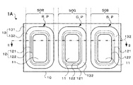
図1は本発明の第1実施形態に係る光学装置の平面図であり、図2はそのII−II線における断面図である。第1実施形態の光学装置は有機ELパネル1Aである。図1および図2に示されるように、有機ELパネル1Aには、RGB3色に対応する複数の発光素子Pが基板10上に配列されている。発光素子Pは画素開口部50(50R,50G,50B)を有する。各画素開口部50は陽極11を底部、絶縁膜12(上面121および側面122)および隔壁層13(上面131および側面132)を側部とし、内側には正孔注入層20および発光層30(30R,30G,30B)が形成される。なお、図1においては、図示の簡易のため、正孔注入層20、発光層30および陰極40を略した。また、図1及び図2にはRGB3色の発光素子Pが3個のみ図示されているが、実際には、多数の発光素子Pが基板10上に配列されている。
Embodiments according to the present invention will be described below with reference to the accompanying drawings. In the drawings, the ratio of dimensions of each part is appropriately changed from the actual one.
<1. Embodiment>
FIG. 1 is a plan view of the optical device according to the first embodiment of the present invention, and FIG. 2 is a sectional view taken along the line II-II. The optical device of the first embodiment is an
図2に示されるように、基板10の上には陽極(画素電極)11が発光素子Pごとに相互に離間して配置される。陽極11は、例えばITO(Indium Tin Oxide)などの透明な部材で形成される。一方、基板10には、必要に応じて配線、駆動用TFT(Thin Film Transistor)、層間絶縁膜などの駆動回路を形成しておく。本実施形態における画素電極は陽極11であり、陽極11は層間絶縁膜のコンタクトホールを通して駆動回路に接続される(図示略)。
As shown in FIG. 2, anodes (pixel electrodes) 11 are arranged on the
基板10の上において隣り合う陽極11に挟まれる領域には親水性の絶縁膜12が積層される。絶縁膜12は、陽極11と接する端部において陽極11を部分的に覆いながら陽極11を囲むように形成される。これにより、陽極11は画素開口部50の底部を構成する。一方、陽極11の端部は、絶縁膜12により部分的に覆われているから、絶縁膜12は、上層に形成される陰極(共通電極)40と陽極11とを絶縁するとともに、隣接する陽極11同士の間を絶縁する。絶縁膜12の材料としては、酸化ケイ素、窒化ケイ素、酸化窒化ケイ素などの無機材料が適している。絶縁膜12には後述の正孔注入溶液が濡れ広がる性質がある。絶縁膜12の膜厚は50〜300nmが好ましい。それ以上の膜厚では、成膜時間が長くなる、後で形成する発光層30の膜厚が画素内で均一になりにくくなる、といった弊害がある。
A hydrophilic
絶縁膜12の上には、隔壁層(バンク)13が積層される。隔壁層13は画素開口部50を画定する手段として機能する。隔壁層13は、例えば、感光性のアクリル、ポリイミドなどの有機材料からなる樹脂を採用することができる。隔壁層13は、水系溶液をはじく一方、有機溶剤は若干はじき難い性質を有する。隔壁層13の膜厚は100〜300nmである。これより薄いと、狙い膜厚に対する膜厚ばらつきの割合が大きくなり過ぎ、開口部の寸法精度を維持できなくなってしまい、これより厚いと、後で形成する発光層30の膜厚が均一になりにくいという弊害がある。
A partition layer (bank) 13 is stacked on the
各画素開口部50には、各陽極11を覆うように正孔注入層20が形成される。正孔注入層20の材料としては、例えば、導電性ポリマーの一種であるPEDOT−PSS(3,4−ポリエチレンジオキシチオフェン/ポリスチレンスルフォン酸:溶質)を水系溶媒により分散させた正孔注入材料溶液(PEDOT−PSS分散液)が用いられる。上述したように、絶縁膜12は親水性であるので、正孔注入材料溶液は陽極11を底面とする画素開口部50の底部全体に濡れ広がる。正孔注入層20の上には、有機EL材料からなる発光層30が形成される。くわえて、隔壁層13および発光層30の上には陰極40が形成される。発光素子Pは、陽極11、正孔注入層20、発光層30及び陰極40から構成される。さらに、図2では省略したが、発光素子Pを外気から保護するための封止がなされる。封止構造としては、いわゆる缶封止、べた封止、あるいは薄膜封止などを用いることができる。
A
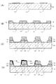
図3および図4に、有機ELパネル1Aの製造工程を示す。まず、図3(A)に示すように基板10の上に陽極11を形成する。この工程では、ITO膜をパターニングすることにより、所定の領域に陽極11を形成する。
3 and 4 show the manufacturing process of the
次に、図3(B)に示すように絶縁膜12を成膜する。材料は酸化ケイ素、窒化ケイ素、酸化窒化ケイ素が適しているが、成膜/エッチングが容易な絶縁材料なら変更可能である。成膜は既知の方法で行なえば良く、方法を限定するものではない。成膜方法としては、例えば、スピンコート、スプレーコート、ロールコート、ダイコート、ディップコート、CVD、スパッタ等がある。絶縁膜12の厚さは、50〜300nmが適している。それ以上の膜厚では、成膜時間が長くなる、エッチング加工精度が悪化する、後で形成する発光層30の膜厚が画素内で均一になりにくくなるという弊害がある。
Next, an insulating
次に、図3(C)に示すように絶縁膜12の上に、感光性のアクリルやポリイミドなどの有機材料を用いて隔壁層13を形成する。隔壁層13は、印刷法やリソグラフィ法等、任意の方法を選択できる。印刷法を使用する場合は、凹版、平版、凸版等任意の方法でバンク形状に有機材料を直接塗布する。リソグラフィ法を使用する場合は、スピンコート、スプレーコート、ロールコート、ダイコート、ディップコート等所定の方法で材料を塗布し、隔壁層13の形状に合わせてマスクを施しレジストを露光・現像することにより所定形状のアクリルやポリイミド樹脂を形成する。最後に焼成して隔壁層13とする。隔壁層13の厚さは0.5μm以下、より望ましくは0.3μm以下である。
Next, as shown in FIG. 3C, a
次に、図3(D)に示すように、隔壁層13の表面に無機層14(14r,14g)を形成する。無機層14は、酸化ケイ素、窒化ケイ素、酸化窒化ケイ素などの無機材料が適している。無機層14は後述するフッ素プラズマ処理によるドライエッチング(気化)により除去される。したがって、フッ素プラズマ処理によりエッチングが可能な材料なら変更可能である。なお、同じ厚みの窒化ケイ素および酸化ケイ素をフッ素プラズマ処理でエッチングした場合、後者の方が前者より早く除去される。よって、酸化ケイ素よりも窒化ケイ素を用いて無機層14を形成した方が処理時間を短縮することができ、さらには、プラズマ処理によって生じる各層へのダメージを低減することができる。
Next, as shown in FIG. 3D, an inorganic layer 14 (14r, 14g) is formed on the surface of the
無機層14r,14gは上述した絶縁膜12と同様の工程で形成される。詳細には、無機層14rは、画素開口部50Rを環状に囲むように隔壁層13の上面131および側面132に形成され、無機層14gは画素開口部50Gを環状に囲むように隔壁層13の上面131および側面132に形成される。また、無機層14rは無機層14gよりも厚い。これにより、無機層14rのエッチングに要する時間は、無機層14gのエッチングに要する時間よりも長い。この一方で、画素開口部50Bを囲む領域には、無機層は形成されない。
The
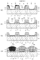
次に、図4(E)に示すように、隔壁層13の上に無機層14が形成された基板10に対してフッ素プラズマ処理を施す。このフッ素プラズマ処理は、フッ素プラズマの被曝露面を撥水化(フッ化)するための処理である。フッ素プラズマ処理が開始されると、隔壁層13の表面のうち、無機層14に覆われることなくむき出しになっている領域がフッ素プラズマに曝され、徐々に撥水化する。一方、無機層14(14r、14g)はフッ素プラズマに曝露されるとエッチングされて除去される。無機層14で覆われていた隔壁層13の領域13r,13gは、無機層14が除去された後にフッ素プラズマに曝されて撥水化する。フッ素プラズマ処理が終了すると、図4(F)に示すような領域13r,13g,13bを有する隔壁層13が形成される。領域13rは、フッ素プラズマ処理前に無機層14rによって覆われていた部分であり、領域13gは、フッ素プラズマ処理前に、無機層14rよりも厚みが少ない無機層14gによって覆われていた部分である。領域13bは、フッ素プラズマ処理開始当初からむき出しになっていた部分である。
Next, as shown in FIG. 4E, fluorine plasma treatment is performed on the
本実施形態では、無機層14の有無および厚みを異ならせることにより領域13r,13g,13bのフッ素プラズマへの曝露時間を適宜調整し、各領域13r,13g,13bの撥水性が制御される。詳細には、隔壁層13の表面のうち無機層14に覆われていた領域13r,13g各々のフッ素プラズマに対する曝露時間は、領域13bの曝露時間よりも短い。よって、フッ素プラズマ処理が終了したときに、その表面の撥水性の程度は、領域13r,13gよりも領域13bの方が高くなる。さらに、領域13rには無機層14rが形成され、領域13gには無機層14rよりも厚みが薄い無機層14gが形成されるから、領域13gは13rと比較して、より早い段階からフッ素プラズマに曝される。よって、フッ素プラズマ処理が終了したときに、領域13rと13gとでは、後者の方が撥水化の程度が高い。このように、各領域13r,13g,13bがフッ素プラズマに曝露される時間の長さはt(13r)<t(13g)<t(13b)なので、撥水化の程度は13r<13g<13bとなる。撥水化の程度が高い方が(液体材料をはじくほど)、濡れ広がり難いので、同一の特性を有する液体材料を各画素に充填したときの液体材料が濡れ広がる程度は、領域13bの方が領域13r,13gよりも小さく、領域13rと13gとでは後者の方が小さい(すなわち、13r>13g>13b)。
In the present embodiment, the exposure time of the
以上のようにして、隔壁層13の表面にそれぞれが異なる撥水性を有する領域13r,13g,13bが形成される。上述したように、領域13rは画素開口部50Rを環状に囲む領域であり、領域13gは画素開口部50Gを環状に囲む領域である。また、領域13bは画素開口部50Gを環状に囲む領域である。
As described above, the
ところで、有機ELパネル1Aの発光層材料溶液として用いるRGB各色の有機EL溶液は、RGBいずれかの色で発光する発光材料を含む。よって、画素開口部50R,50G,50Bに充填される溶液の特性はRGB各色間で同一ではない。各画素開口部に充填される溶液の特性が異なると、同一の撥水性に設定された表面に同量の溶液を流し込んだ場合、溶液の濡れ広がり方が画素によって異なる場合がある。その結果、形成された発光層の膜厚にバラツキが生じ、画素間で輝度がばらついてしまう。このため、本実施形態では、発光層材料溶液の種類(本実施形態では「有機EL溶液の色」)に応じて、撥水性が異なる複数の領域13r,13g,13bを各画素開口部50R,50G,50Bの周りに形成する。これにより、各画素開口部50R,50G,50Bに充填する互いに特性が異なる各有機EL溶液の濡れ広がり方が均一となるように制御している。
By the way, the organic EL solution of each color of RGB used as the light emitting layer material solution of the
次に、図4(G)に示すように、正孔注入材料溶液をインクジェット法によって画素開口部50R,50G,50Bに打ち込み、乾燥させることで正孔注入層20を形成する。正孔注入材料溶液に水系溶媒を用いるから、撥水性の隔壁層13にはじかれる一方、親水性の絶縁膜12になじみ易い。このため、正孔注入材料溶液は各画素開口部50R,50G,50Bの隔壁層13を側部とする部分には付着せず、絶縁膜12を側部とする部分および底部に向かって流れ込み、底部全体に濡れ広がる。
Next, as shown in FIG. 4G, the
その後、図4(H)に示すように、RGB各色の有機EL材料溶液をインクジェット法に拠って各画素開口部50R,50G,50Bに打ち込み、乾燥させることで発光層30R,30G,30Bを形成する。各画素開口部50R,50G,50Bの領域13r,13g,13bの表面は各色の有機EL材料溶液の特性に応じた撥水性に設定されているので、各画素開口部50R,50G,50BにはRGB各色の有機EL材料溶液が均一に濡れ広がり、結果として膜厚のバラツキが少ない発光層30R,30G,30Bが形成される。
Thereafter, as shown in FIG. 4 (H), the organic EL material solutions of RGB colors are driven into the
以上説明したように、本実施形態の有機ELパネル1Aおよびその製造方法によれば、隔壁層13の表面に、有機EL材料溶液の種類に応じて撥水性を相違させた領域13r,13g,13bを形成するので、各色の有機EL材料溶液を流し込んだ場合に、それぞれの濡れ広がり方が均一化される。結果として、発光層30R,30G,30Bの膜厚が均一化され、光ヘッドとして用いた場合には、高品質な印刷結果が得られ、表示装置の場合には、高品位な表示画像が得られる。
As described above, according to the
<2.変形例>
上述した実施形態では、隔壁層13の上面131および側面132に無機層14を形成する態様について説明したが、隔壁層13の上面131にのみ無機層14を形成する態様としてもよい。この場合、画素開口部50R,50G,50Bの内部を除く周縁部が異なる撥水性に設定される。この態様によっても、隔壁層13上面における発光層材料溶液の濡れ広がり方は画素間で均一化されるので、上述した実施形態と同様の効果を得ることが可能である。
<2. Modification>
In the above-described embodiment, the aspect in which the
上述した実施形態では、図3および図4の製造方法を用いて製造する光学装置の例として有機ELパネル1Aを例に挙げて説明したが、同様の方法を用いて、カラーフィルタを製造することができる。この場合、貫通孔を確定する隔壁層としてブラックマトリクスを基板の上に形成した後に、ブラックマトリクスの表面の一部に上記実施形態と同様の無機層14を形成する。そして、ブラックマトリクスの表面にフッ素プラズマ処理により撥水化処理を施し、インクジェットの吐出ヘッドから貫通孔に向けて各色RGBの材料溶液を打ち込む。上記実施形態と同様に、液体材料の種類(色)に応じて無機層14の有無および厚みを異ならせることにより、各貫通孔に充填される異なる種類の液体材料の濡れ広がり方を均一化することが可能となる。
In the above-described embodiment, the
<3.応用例>
次に、本発明に係る光学装置を適用した電子機器について説明する。図4ないし図6には、本発明に係る光学装置を表示装置の一部または全部として採用した電子機器の形態が図示されている。
<3. Application example>
Next, an electronic apparatus to which the optical device according to the present invention is applied will be described. 4 to 6 show forms of electronic devices in which the optical device according to the present invention is used as part or all of a display device.
図4は、本発明に係る光学装置を適用したモバイル型のパーソナルコンピュータの構成を示す斜視図である。パーソナルコンピュータ2000は、各種の画像を表示する表示装置Dと、電源スイッチ2001やキーボード2002が設置された本体部2010とを具備する。表示装置Dが有機ELパネル1Aの場合には、視野角が広く見易い画面を表示できる。
FIG. 4 is a perspective view showing the configuration of a mobile personal computer to which the optical apparatus according to the present invention is applied. The
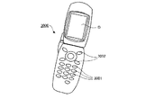
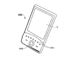
図5は、本発明に係る光学装置を適用した携帯電話機の構成を示す斜視図である。携帯電話機3000は、複数の操作ボタン3001およびスクロールボタン3002と、各種の画像を表示する表示装置Dとを備える。スクロールボタン3002を操作することによって、表示装置Dに表示される画面がスクロールされる。
FIG. 5 is a perspective view showing a configuration of a mobile phone to which the optical device according to the present invention is applied. The
図6は、本発明に係る光学装置を適用した携帯情報端末(PDA:Personal Digital Assistants)の構成を示す斜視図である。情報携帯端末4000は、複数の操作ボタン4001および電源スイッチ4002と、各種の画像を表示する表示装置Dとを備える。電源スイッチ4002を操作すると、住所録やスケジュール帳といった様々な情報が表示装置Dに表示される。
FIG. 6 is a perspective view showing a configuration of a personal digital assistant (PDA) to which the optical device according to the present invention is applied. The information
なお、本発明に係る光学装置が適用される電子機器としては、図4から図6に示した機器のほか、デジタルスチルカメラ、テレビ、ビデオカメラ、カーナビゲーション装置、ページャ、電子手帳、電子ペーパー、電卓、ワードプロセッサ、ワークステーション、テレビ電話、POS端末、プリンタ、スキャナ、複写機、ビデオプレーヤ、タッチパネルを備えた機器等などが挙げられる。 In addition, as an electronic device to which the optical device according to the present invention is applied, in addition to the devices shown in FIGS. 4 to 6, a digital still camera, a television, a video camera, a car navigation device, a pager, an electronic notebook, electronic paper, Examples include calculators, word processors, workstations, videophones, POS terminals, printers, scanners, copiers, video players, devices equipped with touch panels, and the like.
1A…有機ELパネル(光学装置)、10…基板、11…陽極、12,121,122…絶縁膜、13,131,132…隔壁層、13r,13g,13b…領域、14,14r,14g…無機層、20…正孔注入層、30(30R,30G,30B)…発光層、40…陰極、50(50R,50G,50B)…画素開口部(貫通孔)、P…発光素子。
DESCRIPTION OF
Claims (5)
前記隔壁層の上に、無機材料で、前記隔壁層の上面の一部を覆う無機層を形成する第2工程と、
前記隔壁層および前記無機層が形成された前記基板に対してフッ素プラズマ処理を施すことにより前記無機層を除去する第3工程と、
を有する光学装置の製造方法。 Forming a partition layer defining a plurality of through-holes with an organic material on a substrate;
A second step of forming, on the partition layer, an inorganic layer covering an upper surface of the partition layer with an inorganic material;
A third step of removing the inorganic layer by performing a fluorine plasma treatment on the substrate on which the partition layer and the inorganic layer are formed;
A method for manufacturing an optical device.
前記隔壁層の上に、無機材料で、前記隔壁層の上面の一部を覆う層状の第1無機部と、前記第1無機部と異なる厚みを有し、前記隔壁層の上面の他の一部を覆う層状の第2無機部とを形成する第2工程と、
前記隔壁層、前記第1無機部および前記第2無機部が形成された前記基板に対してフッ素プラズマ処理を施すことにより前記第1無機部および前記第2無機部を除去する第3工程と、
を有する光学装置の製造方法。 Forming a partition layer defining a plurality of through-holes with an organic material on a substrate;
A layered first inorganic portion that covers an upper surface of the partition wall layer with an inorganic material on the partition wall layer, and has a thickness different from that of the first inorganic portion, A second step of forming a layered second inorganic part covering the part;
A third step of removing the first inorganic part and the second inorganic part by performing a fluorine plasma treatment on the substrate on which the partition layer, the first inorganic part and the second inorganic part are formed;
A method for manufacturing an optical device.
前記基板の上に、有機材料で形成され、複数の貫通孔を画定している隔壁層とを備え、
前記隔壁層の上面には、撥水性が互いに異なる複数の領域が含まれている、
ことを特徴とする光学装置。 A substrate,
A partition layer formed of an organic material and defining a plurality of through holes on the substrate;
The upper surface of the partition wall layer includes a plurality of regions having different water repellency from each other.
An optical device.
ことを特徴とする請求項3に記載の光学装置。 Each of the plurality of regions is an annular region surrounding the through hole.
The optical apparatus according to claim 3.
An electronic apparatus comprising the optical device according to claim 3.
Priority Applications (1)
| Application Number | Priority Date | Filing Date | Title |
|---|---|---|---|
| JP2006303652A JP2008123738A (en) | 2006-11-09 | 2006-11-09 | Optical device, method of manufacturing optical device, and electronic apparatus. |
Applications Claiming Priority (1)
| Application Number | Priority Date | Filing Date | Title |
|---|---|---|---|
| JP2006303652A JP2008123738A (en) | 2006-11-09 | 2006-11-09 | Optical device, method of manufacturing optical device, and electronic apparatus. |
Publications (1)
| Publication Number | Publication Date |
|---|---|
| JP2008123738A true JP2008123738A (en) | 2008-05-29 |
Family
ID=39508288
Family Applications (1)
| Application Number | Title | Priority Date | Filing Date |
|---|---|---|---|
| JP2006303652A Withdrawn JP2008123738A (en) | 2006-11-09 | 2006-11-09 | Optical device, method of manufacturing optical device, and electronic apparatus. |
Country Status (1)
| Country | Link |
|---|---|
| JP (1) | JP2008123738A (en) |
Cited By (4)
| Publication number | Priority date | Publication date | Assignee | Title |
|---|---|---|---|---|
| JP2010073598A (en) * | 2008-09-22 | 2010-04-02 | Mitsubishi Chemicals Corp | Organic thin film patterning substrate, organic electroluminescent device, organic el display device, and organic el lighting |
| JP2013008697A (en) * | 2009-06-24 | 2013-01-10 | Semiconductor Energy Lab Co Ltd | Illumination device |
| KR101604155B1 (en) | 2008-11-28 | 2016-03-16 | 스미또모 가가꾸 가부시키가이샤 | Light emission device and method for manufacturing same |
| JP2019110115A (en) * | 2017-12-15 | 2019-07-04 | 株式会社Joled | Organic el display panel, organic el display device, and manufacturing method thereof |
-
2006
- 2006-11-09 JP JP2006303652A patent/JP2008123738A/en not_active Withdrawn
Cited By (5)
| Publication number | Priority date | Publication date | Assignee | Title |
|---|---|---|---|---|
| JP2010073598A (en) * | 2008-09-22 | 2010-04-02 | Mitsubishi Chemicals Corp | Organic thin film patterning substrate, organic electroluminescent device, organic el display device, and organic el lighting |
| KR101604155B1 (en) | 2008-11-28 | 2016-03-16 | 스미또모 가가꾸 가부시키가이샤 | Light emission device and method for manufacturing same |
| JP2013008697A (en) * | 2009-06-24 | 2013-01-10 | Semiconductor Energy Lab Co Ltd | Illumination device |
| US8525407B2 (en) | 2009-06-24 | 2013-09-03 | Semiconductor Energy Laboratory Co., Ltd. | Light source and device having the same |
| JP2019110115A (en) * | 2017-12-15 | 2019-07-04 | 株式会社Joled | Organic el display panel, organic el display device, and manufacturing method thereof |
Similar Documents
| Publication | Publication Date | Title |
|---|---|---|
| JP3915806B2 (en) | Electro-optical device and electronic apparatus | |
| JP4924314B2 (en) | Organic EL device and electronic device | |
| KR102009357B1 (en) | Organic electro-luminescent device and method of fabricating the same | |
| CN101800194B (en) | Method of manufacturing display device and display device | |
| JP2008243773A (en) | ELECTROLUMINESCENT DEVICE, ITS MANUFACTURING METHOD, ELECTRONIC DEVICE, THIN FILM STRUCTURE, THIN FILM FORMING METHOD | |
| KR20140067645A (en) | Organic electro-luminescent device and method of fabricating the same | |
| US11302895B2 (en) | Display substrate having separation pillar in the peripheral area, display apparatus, and method of fabricating display substrate having the same | |
| JP2019504434A (en) | Touch screen, method of manufacturing the same, and display device | |
| JP4556566B2 (en) | Electro-optical device and electronic apparatus | |
| US11233115B2 (en) | Display panel and manufacturing method thereof, and display device | |
| CN111682052A (en) | Display substrate and preparation method thereof, display panel, and display device | |
| JP2008234989A (en) | Organic electroluminescence device and line head | |
| KR20140110497A (en) | Organic electro-luminescent device | |
| CN110660839B (en) | A display panel and its manufacturing method | |
| US20100271353A1 (en) | Semiconductor device, production method of semiconductor device, display device, and electronic equipment | |
| CN110085626B (en) | Display device and method of manufacturing the same | |
| JP5266737B2 (en) | Organic EL device and electronic device | |
| JP4957477B2 (en) | Manufacturing method of organic EL device | |
| JP2011096376A (en) | Optical device, method of manufacturing the same, and electronic apparatus | |
| JP2007095608A (en) | Electro-optical device, electronic apparatus, and method of manufacturing electro-optical device | |
| JP5119635B2 (en) | Manufacturing method of display device | |
| CN111785852B (en) | A display substrate, its manufacturing method, display panel and display device | |
| JP2008112658A (en) | Electro-optical device, electronic device, color filter device, and image display device | |
| JP4899333B2 (en) | Electro-optical device, method of manufacturing electro-optical device, and electronic apparatus | |
| JP4978543B2 (en) | Organic electroluminescence device and manufacturing method thereof |
Legal Events
| Date | Code | Title | Description |
|---|---|---|---|
| A621 | Written request for application examination |
Free format text: JAPANESE INTERMEDIATE CODE: A621 Effective date: 20090703 |
|
| A761 | Written withdrawal of application |
Free format text: JAPANESE INTERMEDIATE CODE: A761 Effective date: 20110125 |