JP2008193003A - 光モジュール - Google Patents
光モジュール Download PDFInfo
- Publication number
- JP2008193003A JP2008193003A JP2007028588A JP2007028588A JP2008193003A JP 2008193003 A JP2008193003 A JP 2008193003A JP 2007028588 A JP2007028588 A JP 2007028588A JP 2007028588 A JP2007028588 A JP 2007028588A JP 2008193003 A JP2008193003 A JP 2008193003A
- Authority
- JP
- Japan
- Prior art keywords
- optical
- element unit
- optical module
- optical element
- resonator
- Prior art date
- Legal status (The legal status is an assumption and is not a legal conclusion. Google has not performed a legal analysis and makes no representation as to the accuracy of the status listed.)
- Granted
Links
Images

Classifications
-
- H—ELECTRICITY
- H01—ELECTRIC ELEMENTS
- H01S—DEVICES USING THE PROCESS OF LIGHT AMPLIFICATION BY STIMULATED EMISSION OF RADIATION [LASER] TO AMPLIFY OR GENERATE LIGHT; DEVICES USING STIMULATED EMISSION OF ELECTROMAGNETIC RADIATION IN WAVE RANGES OTHER THAN OPTICAL
- H01S5/00—Semiconductor lasers
- H01S5/02—Structural details or components not essential to laser action
- H01S5/024—Arrangements for thermal management
- H01S5/02407—Active cooling, e.g. the laser temperature is controlled by a thermo-electric cooler or water cooling
- H01S5/02415—Active cooling, e.g. the laser temperature is controlled by a thermo-electric cooler or water cooling by using a thermo-electric cooler [TEC], e.g. Peltier element
-
- G—PHYSICS
- G02—OPTICS
- G02B—OPTICAL ELEMENTS, SYSTEMS OR APPARATUS
- G02B6/00—Light guides; Structural details of arrangements comprising light guides and other optical elements, e.g. couplings
- G02B6/10—Light guides; Structural details of arrangements comprising light guides and other optical elements, e.g. couplings of the optical waveguide type
- G02B6/12—Light guides; Structural details of arrangements comprising light guides and other optical elements, e.g. couplings of the optical waveguide type of the integrated circuit kind
- G02B6/12007—Light guides; Structural details of arrangements comprising light guides and other optical elements, e.g. couplings of the optical waveguide type of the integrated circuit kind forming wavelength selective elements, e.g. multiplexer, demultiplexer
-
- G—PHYSICS
- G02—OPTICS
- G02B—OPTICAL ELEMENTS, SYSTEMS OR APPARATUS
- G02B6/00—Light guides; Structural details of arrangements comprising light guides and other optical elements, e.g. couplings
- G02B6/24—Coupling light guides
- G02B6/42—Coupling light guides with opto-electronic elements
- G02B6/4201—Packages, e.g. shape, construction, internal or external details
-
- G—PHYSICS
- G02—OPTICS
- G02B—OPTICAL ELEMENTS, SYSTEMS OR APPARATUS
- G02B6/00—Light guides; Structural details of arrangements comprising light guides and other optical elements, e.g. couplings
- G02B6/24—Coupling light guides
- G02B6/42—Coupling light guides with opto-electronic elements
- G02B6/4201—Packages, e.g. shape, construction, internal or external details
- G02B6/4204—Packages, e.g. shape, construction, internal or external details the coupling comprising intermediate optical elements, e.g. lenses, holograms
- G02B6/4215—Packages, e.g. shape, construction, internal or external details the coupling comprising intermediate optical elements, e.g. lenses, holograms the intermediate optical elements being wavelength selective optical elements, e.g. variable wavelength optical modules or wavelength lockers
-
- G—PHYSICS
- G02—OPTICS
- G02B—OPTICAL ELEMENTS, SYSTEMS OR APPARATUS
- G02B6/00—Light guides; Structural details of arrangements comprising light guides and other optical elements, e.g. couplings
- G02B6/24—Coupling light guides
- G02B6/42—Coupling light guides with opto-electronic elements
- G02B6/4201—Packages, e.g. shape, construction, internal or external details
- G02B6/4266—Thermal aspects, temperature control or temperature monitoring
- G02B6/4267—Reduction of thermal stress, e.g. by selecting thermal coefficient of materials
-
- G—PHYSICS
- G02—OPTICS
- G02B—OPTICAL ELEMENTS, SYSTEMS OR APPARATUS
- G02B6/00—Light guides; Structural details of arrangements comprising light guides and other optical elements, e.g. couplings
- G02B6/24—Coupling light guides
- G02B6/42—Coupling light guides with opto-electronic elements
- G02B6/4201—Packages, e.g. shape, construction, internal or external details
- G02B6/4266—Thermal aspects, temperature control or temperature monitoring
- G02B6/4268—Cooling
-
- G—PHYSICS
- G02—OPTICS
- G02B—OPTICAL ELEMENTS, SYSTEMS OR APPARATUS
- G02B6/00—Light guides; Structural details of arrangements comprising light guides and other optical elements, e.g. couplings
- G02B6/24—Coupling light guides
- G02B6/42—Coupling light guides with opto-electronic elements
- G02B6/4201—Packages, e.g. shape, construction, internal or external details
- G02B6/4266—Thermal aspects, temperature control or temperature monitoring
- G02B6/4268—Cooling
- G02B6/4271—Cooling with thermo electric cooling
-
- H—ELECTRICITY
- H01—ELECTRIC ELEMENTS
- H01S—DEVICES USING THE PROCESS OF LIGHT AMPLIFICATION BY STIMULATED EMISSION OF RADIATION [LASER] TO AMPLIFY OR GENERATE LIGHT; DEVICES USING STIMULATED EMISSION OF ELECTROMAGNETIC RADIATION IN WAVE RANGES OTHER THAN OPTICAL
- H01S3/00—Lasers, i.e. devices using stimulated emission of electromagnetic radiation in the infrared, visible or ultraviolet wave range
- H01S3/05—Construction or shape of optical resonators; Accommodation of active medium therein; Shape of active medium
- H01S3/08—Construction or shape of optical resonators or components thereof
- H01S3/081—Construction or shape of optical resonators or components thereof comprising three or more reflectors
- H01S3/083—Ring lasers
-
- H—ELECTRICITY
- H01—ELECTRIC ELEMENTS
- H01S—DEVICES USING THE PROCESS OF LIGHT AMPLIFICATION BY STIMULATED EMISSION OF RADIATION [LASER] TO AMPLIFY OR GENERATE LIGHT; DEVICES USING STIMULATED EMISSION OF ELECTROMAGNETIC RADIATION IN WAVE RANGES OTHER THAN OPTICAL
- H01S5/00—Semiconductor lasers
- H01S5/02—Structural details or components not essential to laser action
- H01S5/022—Mountings; Housings
- H01S5/023—Mount members, e.g. sub-mount members
- H01S5/02325—Mechanically integrated components on mount members or optical micro-benches
-
- H—ELECTRICITY
- H01—ELECTRIC ELEMENTS
- H01S—DEVICES USING THE PROCESS OF LIGHT AMPLIFICATION BY STIMULATED EMISSION OF RADIATION [LASER] TO AMPLIFY OR GENERATE LIGHT; DEVICES USING STIMULATED EMISSION OF ELECTROMAGNETIC RADIATION IN WAVE RANGES OTHER THAN OPTICAL
- H01S5/00—Semiconductor lasers
- H01S5/02—Structural details or components not essential to laser action
- H01S5/024—Arrangements for thermal management
- H01S5/02438—Characterized by cooling of elements other than the laser chip, e.g. an optical element being part of an external cavity or a collimating lens
-
- H—ELECTRICITY
- H01—ELECTRIC ELEMENTS
- H01S—DEVICES USING THE PROCESS OF LIGHT AMPLIFICATION BY STIMULATED EMISSION OF RADIATION [LASER] TO AMPLIFY OR GENERATE LIGHT; DEVICES USING STIMULATED EMISSION OF ELECTROMAGNETIC RADIATION IN WAVE RANGES OTHER THAN OPTICAL
- H01S5/00—Semiconductor lasers
- H01S5/06—Arrangements for controlling the laser output parameters, e.g. by operating on the active medium
- H01S5/0607—Arrangements for controlling the laser output parameters, e.g. by operating on the active medium by varying physical parameters other than the potential of the electrodes, e.g. by an electric or magnetic field, mechanical deformation, pressure, light, temperature
- H01S5/0612—Arrangements for controlling the laser output parameters, e.g. by operating on the active medium by varying physical parameters other than the potential of the electrodes, e.g. by an electric or magnetic field, mechanical deformation, pressure, light, temperature controlled by temperature
-
- H—ELECTRICITY
- H01—ELECTRIC ELEMENTS
- H01S—DEVICES USING THE PROCESS OF LIGHT AMPLIFICATION BY STIMULATED EMISSION OF RADIATION [LASER] TO AMPLIFY OR GENERATE LIGHT; DEVICES USING STIMULATED EMISSION OF ELECTROMAGNETIC RADIATION IN WAVE RANGES OTHER THAN OPTICAL
- H01S5/00—Semiconductor lasers
- H01S5/10—Construction or shape of the optical resonator, e.g. extended or external cavity, coupled cavities, bent-guide, varying width, thickness or composition of the active region
- H01S5/14—External cavity lasers
- H01S5/141—External cavity lasers using a wavelength selective device, e.g. a grating or etalon
- H01S5/142—External cavity lasers using a wavelength selective device, e.g. a grating or etalon which comprises an additional resonator
Landscapes
- Physics & Mathematics (AREA)
- General Physics & Mathematics (AREA)
- Optics & Photonics (AREA)
- Engineering & Computer Science (AREA)
- Microelectronics & Electronic Packaging (AREA)
- Condensed Matter Physics & Semiconductors (AREA)
- Electromagnetism (AREA)
- Semiconductor Lasers (AREA)
- Optical Couplings Of Light Guides (AREA)
- Optical Modulation, Optical Deflection, Nonlinear Optics, Optical Demodulation, Optical Logic Elements (AREA)
- Optical Integrated Circuits (AREA)
Abstract
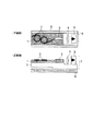
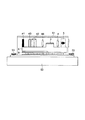
【解決手段】光素子ユニット7の底面全体にかけて温度制御素子であるペルチェ素子8を配置すると共に、光素子ユニット7とペルチェ素子8とを、光素子ユニット7の底面の一部分で接合し、外部共振器2の共振波長を決定しているリング共振器部分をペルチェ素子8と接触させずに浮かして空間層を形成する。
【選択図】図1
Description
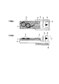
2 光共振器
3 SOA(半導体光増幅器)
4 レンズ
5 アイソレータ
6 キャリア
7 光素子ユニット
8 ペルチェ素子
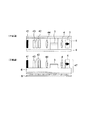
41 反射ミラー
42 波長選択素子
43 光路長調整器
44 レンズ
47 光素子ユニット
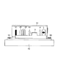
51 パッケージ
52 ヒートシンク
53 ネジ
Claims (11)
- 光導波路と光素子とをハイブリット集積してなる光素子ユニットと、前記光素子ユニットの温度を制御するための温度制御素子とを有し、
前記光素子ユニットと前記温度制御素子とが、前記光素子ユニットにおける前記光導波路以外の他の部分に対応する底面の一部分で接合されたことを特徴とする光モジュール。 - 共振波長を可変制御可能な光共振器を備えた光素子ユニットと、前記光素子ユニットの温度を制御するための温度制御素子とを有し、
前記光素子ユニットと前記温度制御素子とが、前記光素子ユニットにおける前記光共振器以外の他の部分に対応する底面の一部分で接合されたことを特徴とする光モジュール。 - 前記請求項1又は2に記載の光モジュールにおいて、
前記光素子ユニットが、光導波路で構成されたリング共振器を含むことを特徴とする光モジュール。 - 前記請求項2に記載の光モジュールにおいて、
前記光共振器が、特定の波長の光線を透過する波長選択素子と、光路長を調整する光路長調整器とを有した構成であることを特徴とする光モジュール。 - 前記請求項1乃至4のいずれか一項に記載の光モジュールにおいて、
前記光素子ユニットと前記温度制御素子との間の接合されていない部分に空間層を形成したことを特徴とする光モジュール。 - 前記請求項1乃至5のいずれか一項に記載の光モジュールにおいて、
前記温度制御素子が、前記光素子ユニットの底面全体にかけて配置されたことを特徴とする光モジュール。 - 光導波路と光素子とをハイブリット集積してなる光素子ユニットがパッケージ内に実装された構成の光モジュールであって、
前記光素子ユニットにおける前記光導波路以外の他の部分に対応する底面の一部分が、前記パッケージと接合固定されたことを特徴とする光モジュール。 - 共振波長を可変制御可能な光共振器を備えた光素子ユニットが、パッケージ内に実装された構成の光モジュールであって、
前記光素子ユニットにおける前記光共振器以外の他の部分に対応する底面の一部分が、前記パッケージと接合固定されたことを特徴とする光モジュール。 - 前記請求項7又は8に記載の光モジュールにおいて、
前記光素子ユニットが、光導波路で構成されたリング共振器を含むことを特徴とする光モジュール。 - 前記請求項8に記載の光モジュールにおいて、
前記光共振器が、特定の波長の光線を透過する波長選択素子と、光路長を調整する光路長調整器とを有した構成であることを特徴とする光モジュール。 - 前記請求項7乃至10のいずれか一項に記載の光モジュールにおいて、
前記光素子ユニットと前記パッケージとの間の接合されていない部分に空間層を形成したことを特徴とする光モジュール。
Priority Applications (5)
| Application Number | Priority Date | Filing Date | Title |
|---|---|---|---|
| JP2007028588A JP5050548B2 (ja) | 2007-02-07 | 2007-02-07 | 光モジュール |
| TW097100713A TW200849750A (en) | 2007-02-07 | 2008-01-08 | Optical module |
| US12/016,300 US7585117B2 (en) | 2007-02-07 | 2008-01-18 | Optical module |
| CN2008100053592A CN101286619B (zh) | 2007-02-07 | 2008-02-01 | 光学模块 |
| EP08002058A EP1956402A1 (en) | 2007-02-07 | 2008-02-04 | Optical module |
Applications Claiming Priority (1)
| Application Number | Priority Date | Filing Date | Title |
|---|---|---|---|
| JP2007028588A JP5050548B2 (ja) | 2007-02-07 | 2007-02-07 | 光モジュール |
Publications (2)
| Publication Number | Publication Date |
|---|---|
| JP2008193003A true JP2008193003A (ja) | 2008-08-21 |
| JP5050548B2 JP5050548B2 (ja) | 2012-10-17 |
Family
ID=39339818
Family Applications (1)
| Application Number | Title | Priority Date | Filing Date |
|---|---|---|---|
| JP2007028588A Expired - Fee Related JP5050548B2 (ja) | 2007-02-07 | 2007-02-07 | 光モジュール |
Country Status (5)
| Country | Link |
|---|---|
| US (1) | US7585117B2 (ja) |
| EP (1) | EP1956402A1 (ja) |
| JP (1) | JP5050548B2 (ja) |
| CN (1) | CN101286619B (ja) |
| TW (1) | TW200849750A (ja) |
Cited By (8)
| Publication number | Priority date | Publication date | Assignee | Title |
|---|---|---|---|---|
| WO2009101902A1 (ja) * | 2008-02-12 | 2009-08-20 | Nec Corporation | 振動抑制構造 |
| JP2011003807A (ja) * | 2009-06-19 | 2011-01-06 | Nec Corp | 導波路型波長ロッカー及びその製造方法 |
| WO2013191213A1 (ja) * | 2012-06-22 | 2013-12-27 | 古河電気工業株式会社 | 光素子モジュール |
| WO2017047069A1 (ja) * | 2015-09-15 | 2017-03-23 | 日本電気株式会社 | 光源モジュール、および光源モジュールの製造方法 |
| WO2020157853A1 (ja) * | 2019-01-30 | 2020-08-06 | 三菱電機株式会社 | 光送信モジュール |
| WO2020162446A1 (ja) * | 2019-02-08 | 2020-08-13 | 古河電気工業株式会社 | 光モジュール |
| JP2022521709A (ja) * | 2019-02-12 | 2022-04-12 | ラボラトリオ・エウロペオ・ディ・スペットロスコピエ・ノン・リネアリ(エッレエエンネエッセ) | 外部共振器レーザ装置、対応するシステム及び方法 |
| JPWO2023084594A1 (ja) * | 2021-11-09 | 2023-05-19 |
Families Citing this family (16)
| Publication number | Priority date | Publication date | Assignee | Title |
|---|---|---|---|---|
| US7231113B2 (en) * | 2005-08-19 | 2007-06-12 | Infinera Corporation | Coupled optical waveguide resonators with heaters for thermo-optic control of wavelength and compound filter shape |
| JP4877009B2 (ja) * | 2007-03-28 | 2012-02-15 | 日本電気株式会社 | Wdm光伝送用光直接増幅器 |
| JP2008270583A (ja) * | 2007-04-23 | 2008-11-06 | Nec Corp | 波長可変光源装置とその制御方法,制御用プログラム |
| US8337096B2 (en) * | 2009-11-30 | 2012-12-25 | Futurewei Technologies, Inc. | Efficient thermoelectric cooling of photonic integrated circuits |
| JP5693888B2 (ja) * | 2010-07-28 | 2015-04-01 | 住友電工デバイス・イノベーション株式会社 | 光デバイスおよびその製造方法 |
| JP6056118B2 (ja) * | 2011-03-23 | 2017-01-11 | セイコーエプソン株式会社 | 光学モジュール及び原子発振器 |
| CN102402024A (zh) * | 2011-11-15 | 2012-04-04 | 浙江大学 | 一种能实现无温度效应的集成电光相位调制器 |
| WO2017010570A1 (ja) * | 2015-07-16 | 2017-01-19 | 古河電気工業株式会社 | 半導体レーザモジュール |
| JP2017032629A (ja) * | 2015-07-29 | 2017-02-09 | 住友電気工業株式会社 | 光モジュール |
| JP6500750B2 (ja) | 2015-11-05 | 2019-04-17 | 住友電気工業株式会社 | 半導体光素子、半導体組立体 |
| CN105589161A (zh) * | 2015-12-18 | 2016-05-18 | 中国科学技术大学 | 一种可调恒温滤光片切换装置 |
| CN106980159B (zh) * | 2017-03-07 | 2019-01-22 | 中国科学院微电子研究所 | 基于光电混合集成的光电模块封装结构 |
| WO2019199936A1 (en) * | 2018-04-12 | 2019-10-17 | Raytheon Company | Integrated optical resonant detector |
| JP7110386B2 (ja) | 2018-04-12 | 2022-08-01 | レイセオン カンパニー | 光信号における位相変化検出 |
| JP7211017B2 (ja) | 2018-11-02 | 2023-01-24 | 株式会社デンソー | 光フィルタ、それを用いたレーザ光源および光送受信装置 |
| KR102899215B1 (ko) * | 2020-06-03 | 2025-12-10 | 삼성전자주식회사 | 파장 가변 레이저 광원 및 이를 포함하는 광 조향 장치 |
Citations (3)
| Publication number | Priority date | Publication date | Assignee | Title |
|---|---|---|---|---|
| JP2002131585A (ja) * | 2000-10-20 | 2002-05-09 | Furukawa Electric Co Ltd:The | 半導体レーザモジュールおよびその半導体レーザモジュールを用いたラマンアンプ |
| JP2006278769A (ja) * | 2005-03-29 | 2006-10-12 | Nec Corp | 波長可変レーザ |
| WO2007007848A1 (ja) * | 2005-07-13 | 2007-01-18 | Nec Corporation | 外部共振器型波長可変レーザ及びその実装方法 |
Family Cites Families (8)
| Publication number | Priority date | Publication date | Assignee | Title |
|---|---|---|---|---|
| JPS6282761U (ja) | 1985-11-13 | 1987-05-27 | ||
| US5068865A (en) * | 1988-06-09 | 1991-11-26 | Nec Corporation | Semiconductor laser module |
| GB2376532A (en) | 2001-06-15 | 2002-12-18 | Kymata Ltd | Thermally controlled optical resonator |
| JP3804629B2 (ja) * | 2002-04-25 | 2006-08-02 | ヤマハ株式会社 | 熱電装置用パッケージ |
| JP2004288669A (ja) * | 2003-03-19 | 2004-10-14 | Mitsubishi Electric Corp | 光半導体素子モジュール |
| JP4700563B2 (ja) | 2005-06-15 | 2011-06-15 | 株式会社日立国際電気 | データ伝送方法およびデータ伝送システム |
| CN1322641C (zh) * | 2005-06-22 | 2007-06-20 | 中国科学院上海光学精密机械研究所 | 分布反馈单纵模光纤激光器 |
| JP4505403B2 (ja) * | 2005-11-15 | 2010-07-21 | 富士通株式会社 | 光送信装置 |
-
2007
- 2007-02-07 JP JP2007028588A patent/JP5050548B2/ja not_active Expired - Fee Related
-
2008
- 2008-01-08 TW TW097100713A patent/TW200849750A/zh unknown
- 2008-01-18 US US12/016,300 patent/US7585117B2/en active Active
- 2008-02-01 CN CN2008100053592A patent/CN101286619B/zh not_active Expired - Fee Related
- 2008-02-04 EP EP08002058A patent/EP1956402A1/en not_active Withdrawn
Patent Citations (3)
| Publication number | Priority date | Publication date | Assignee | Title |
|---|---|---|---|---|
| JP2002131585A (ja) * | 2000-10-20 | 2002-05-09 | Furukawa Electric Co Ltd:The | 半導体レーザモジュールおよびその半導体レーザモジュールを用いたラマンアンプ |
| JP2006278769A (ja) * | 2005-03-29 | 2006-10-12 | Nec Corp | 波長可変レーザ |
| WO2007007848A1 (ja) * | 2005-07-13 | 2007-01-18 | Nec Corporation | 外部共振器型波長可変レーザ及びその実装方法 |
Cited By (18)
| Publication number | Priority date | Publication date | Assignee | Title |
|---|---|---|---|---|
| WO2009101902A1 (ja) * | 2008-02-12 | 2009-08-20 | Nec Corporation | 振動抑制構造 |
| JP2011003807A (ja) * | 2009-06-19 | 2011-01-06 | Nec Corp | 導波路型波長ロッカー及びその製造方法 |
| WO2013191213A1 (ja) * | 2012-06-22 | 2013-12-27 | 古河電気工業株式会社 | 光素子モジュール |
| JPWO2013191213A1 (ja) * | 2012-06-22 | 2016-05-26 | 古河電気工業株式会社 | 光素子モジュール |
| US9466942B2 (en) | 2012-06-22 | 2016-10-11 | Furukawa Electric Co., Ltd. | Optical element module |
| WO2017047069A1 (ja) * | 2015-09-15 | 2017-03-23 | 日本電気株式会社 | 光源モジュール、および光源モジュールの製造方法 |
| US10644478B2 (en) | 2015-09-15 | 2020-05-05 | Nec Corporation | Light source module and method of manufacturing light source module |
| WO2020157853A1 (ja) * | 2019-01-30 | 2020-08-06 | 三菱電機株式会社 | 光送信モジュール |
| WO2020162446A1 (ja) * | 2019-02-08 | 2020-08-13 | 古河電気工業株式会社 | 光モジュール |
| JPWO2020162446A1 (ja) * | 2019-02-08 | 2021-12-09 | 古河電気工業株式会社 | 光モジュール |
| US12066657B2 (en) | 2019-02-08 | 2024-08-20 | Furukawa Electric Co., Ltd. | Optical module |
| JP7536657B2 (ja) | 2019-02-08 | 2024-08-20 | 古河電気工業株式会社 | 光モジュール |
| JP2022521709A (ja) * | 2019-02-12 | 2022-04-12 | ラボラトリオ・エウロペオ・ディ・スペットロスコピエ・ノン・リネアリ(エッレエエンネエッセ) | 外部共振器レーザ装置、対応するシステム及び方法 |
| JP7457723B2 (ja) | 2019-02-12 | 2024-03-28 | ラボラトリオ・エウロペオ・ディ・スペットロスコピエ・ノン・リネアリ(エッレエエンネエッセ) | 外部共振器レーザ装置、対応するシステム及び方法 |
| US12132291B2 (en) | 2019-02-12 | 2024-10-29 | Laboratorio Europeo Di Spettroscopie Non Lineari (Lens) | External-cavity laser device, corresponding system and method |
| JPWO2023084594A1 (ja) * | 2021-11-09 | 2023-05-19 | ||
| WO2023084594A1 (ja) * | 2021-11-09 | 2023-05-19 | 日本電気株式会社 | 制御装置、光源装置、送信モジュール、光トランシーバ、および制御方法 |
| JP7694692B2 (ja) | 2021-11-09 | 2025-06-18 | 日本電気株式会社 | 制御装置、光源装置、光送信モジュール、光トランシーバ、および制御方法 |
Also Published As
| Publication number | Publication date |
|---|---|
| US7585117B2 (en) | 2009-09-08 |
| CN101286619A (zh) | 2008-10-15 |
| JP5050548B2 (ja) | 2012-10-17 |
| TW200849750A (en) | 2008-12-16 |
| CN101286619B (zh) | 2012-07-18 |
| US20080187268A1 (en) | 2008-08-07 |
| EP1956402A1 (en) | 2008-08-13 |
Similar Documents
| Publication | Publication Date | Title |
|---|---|---|
| JP5050548B2 (ja) | 光モジュール | |
| US6101210A (en) | External cavity laser | |
| US20100177793A1 (en) | Passive Phase Control in an External Cavity Laser | |
| JPWO2019193706A1 (ja) | 光モジュール | |
| JP7536657B2 (ja) | 光モジュール | |
| US7869475B2 (en) | Misalignment prevention in an external cavity laser having temperature stabilisation of the resonator and the gain medium | |
| JP2019140306A (ja) | 光モジュール | |
| CA2717476C (en) | Optical module | |
| JP2008197500A (ja) | 光モジュール | |
| JP2013197256A (ja) | 半導体レーザモジュール及びその製造方法 | |
| JP3326761B2 (ja) | 周波数可変光源モジュール | |
| HK1124180A (en) | Optical module | |
| JP2006003651A (ja) | 光モジュール及び光モジュールの製造方法 | |
| JP3857930B2 (ja) | 光導波路モジュール | |
| JP5182602B2 (ja) | 可変分散補償器 | |
| JP2001021743A (ja) | 温度無依存光波回路型デバイス | |
| JP2001324629A (ja) | アレイ導波路型回折格子 | |
| HK1125183A (en) | Optical module | |
| JP2003240987A (ja) | 光導波路モジュール | |
| JP2004198547A (ja) | 光モジュール | |
| JP2006215585A (ja) | 光導波路モジュール |
Legal Events
| Date | Code | Title | Description |
|---|---|---|---|
| A621 | Written request for application examination |
Free format text: JAPANESE INTERMEDIATE CODE: A621 Effective date: 20100119 |
|
| A977 | Report on retrieval |
Free format text: JAPANESE INTERMEDIATE CODE: A971007 Effective date: 20110720 |
|
| A131 | Notification of reasons for refusal |
Free format text: JAPANESE INTERMEDIATE CODE: A131 Effective date: 20110726 |
|
| A521 | Request for written amendment filed |
Free format text: JAPANESE INTERMEDIATE CODE: A523 Effective date: 20110922 |
|
| A131 | Notification of reasons for refusal |
Free format text: JAPANESE INTERMEDIATE CODE: A131 Effective date: 20120228 |
|
| A521 | Request for written amendment filed |
Free format text: JAPANESE INTERMEDIATE CODE: A523 Effective date: 20120319 |
|
| TRDD | Decision of grant or rejection written | ||
| A01 | Written decision to grant a patent or to grant a registration (utility model) |
Free format text: JAPANESE INTERMEDIATE CODE: A01 Effective date: 20120626 |
|
| A01 | Written decision to grant a patent or to grant a registration (utility model) |
Free format text: JAPANESE INTERMEDIATE CODE: A01 |
|
| A61 | First payment of annual fees (during grant procedure) |
Free format text: JAPANESE INTERMEDIATE CODE: A61 Effective date: 20120709 |
|
| R150 | Certificate of patent or registration of utility model |
Ref document number: 5050548 Country of ref document: JP Free format text: JAPANESE INTERMEDIATE CODE: R150 Free format text: JAPANESE INTERMEDIATE CODE: R150 |
|
| FPAY | Renewal fee payment (event date is renewal date of database) |
Free format text: PAYMENT UNTIL: 20150803 Year of fee payment: 3 |
|
| LAPS | Cancellation because of no payment of annual fees |