JP2008204792A - Organic electroluminescence device and method for manufacturing the same - Google Patents
Organic electroluminescence device and method for manufacturing the same Download PDFInfo
- Publication number
- JP2008204792A JP2008204792A JP2007039404A JP2007039404A JP2008204792A JP 2008204792 A JP2008204792 A JP 2008204792A JP 2007039404 A JP2007039404 A JP 2007039404A JP 2007039404 A JP2007039404 A JP 2007039404A JP 2008204792 A JP2008204792 A JP 2008204792A
- Authority
- JP
- Japan
- Prior art keywords
- light emitting
- organic
- layer
- hole transport
- pixel electrode
- Prior art date
- Legal status (The legal status is an assumption and is not a legal conclusion. Google has not performed a legal analysis and makes no representation as to the accuracy of the status listed.)
- Granted
Links
Images
Landscapes
- Electroluminescent Light Sources (AREA)
Abstract
【課題】正孔輸送層が絶縁層と画素電極が接する縁部において厚膜化するのを抑制し、発光ムラや輝度低下をなくした均一性の良い表示を行うことが可能な有機EL素子の製造方法およびこれにより製造された有機EL素子を提供する。
【解決手段】画素電極2と、画素電極2上に発光領域を画定する絶縁層3と、発光領域に積層されかつ少なくとも正孔輸送層4及び有機発光層5の2層を含む有機発光媒体層と、対向電極6とからなる有機エレクトロルミネッセンス素子の製造方法であって、発光領域内に、正孔輸送材料を溶媒に溶解または分散させた正孔輸送インキを凸版印刷法により凸版の凸部から絶縁層3の間にある画素電極2に印刷して正孔輸送層4を形成する工程を備え、その際、凸版の上で正孔輸送インキが半乾燥する時間を設ける。
【選択図】図1An organic EL device capable of suppressing the increase in thickness of a hole transport layer at an edge where an insulating layer and a pixel electrode are in contact with each other and eliminating unevenness of light emission and lowering in luminance and displaying with good uniformity. A production method and an organic EL device produced thereby are provided.
An organic light emitting medium layer comprising a pixel electrode, an insulating layer defining a light emitting region on the pixel electrode, and at least two layers of a hole transporting layer and an organic light emitting layer stacked on the light emitting region. And a method for producing an organic electroluminescence element comprising a counter electrode 6, wherein a hole transport ink in which a hole transport material is dissolved or dispersed in a solvent is formed in a light emitting region from a convex portion of a relief plate by a relief printing method. A step of forming the hole transport layer 4 by printing on the pixel electrode 2 between the insulating layers 3 is provided, and at this time, a time for the hole transport ink to be semi-dried on the relief printing is provided.
[Selection] Figure 1
Description
本発明は、有機エレクトロルミネッセンス(EL)ディスプレイパネル等に用いられる有機EL素子とその製造方法に関し、特に有機発光媒体層を印刷法によって形成する有機EL素子及びその製造方法に関する。 The present invention relates to an organic EL element used for an organic electroluminescence (EL) display panel and the like and a manufacturing method thereof, and more particularly to an organic EL element in which an organic light emitting medium layer is formed by a printing method and a manufacturing method thereof.
有機EL素子は、二つの対向する電極の間に有機発光材料からなる有機発光層が形成され、有機発光層に電流を流すことで発光させるものであるが、効率よく発光させるには有機発光層の膜厚が重要であり、100nm程度の薄膜にする必要がある。さらに、これをディスプレイパネル化するには高精細にパターニングする必要がある。 An organic EL element is one in which an organic light emitting layer made of an organic light emitting material is formed between two opposing electrodes, and light is emitted by passing a current through the organic light emitting layer. The film thickness is important, and it is necessary to form a thin film of about 100 nm. Furthermore, in order to make this a display panel, it is necessary to pattern it with high definition.
有機発光層を形成する有機発光材料には、低分子材料と高分子材料が有り、一般に低分子材料は真空蒸着法等により薄膜形成し、このときに微細パターンのマスクを用いてパターニングするが、この方法では基板が大型化すればするほどパターニング精度が出にくいという問題がある。また、真空中で成膜するためにスループットが悪いという問題がある。 The organic light emitting material for forming the organic light emitting layer includes a low molecular material and a high molecular material. Generally, a low molecular material is formed into a thin film by a vacuum deposition method or the like, and is patterned using a fine pattern mask at this time. This method has a problem that the larger the substrate is, the less patterning accuracy is obtained. In addition, since the film is formed in a vacuum, there is a problem that the throughput is poor.
そこで、最近では高分子材料を溶剤に溶かして塗工液にし、これをウェットコーティング法で薄膜形成する方法が試みられるようになってきている。高分子材料の塗工液を用いてウェットコーティング法で有機発光媒体層を形成する場合の層構成は、陽極側から正孔輸送層、有機発光層と積層する二層構成が一般的である。このとき、有機発光層はカラーパネル化するために赤(R)、緑(G)、青(B)のそれぞれの発光色をもつ有機発光材料を溶剤中に溶解または安定して分散してなる有機発光インキを用いて塗り分ける必要がある。塗り分けの方法としては、オフセット印刷法が提案されている。(例えば特許文献1参照)。
また、微細パターンを形成する他の方法としては、凸版印刷法が提案されており、例えば特許文献2において、基板上に半導体回路パターンを形成する技術が開示されている。
As another method for forming a fine pattern, a relief printing method has been proposed. For example, Patent Document 2 discloses a technique for forming a semiconductor circuit pattern on a substrate.
上記の如き構成の有機EL素子を有する有機ELディスプレイパネルにおいて、正孔輸送層はパターニングせずに、画像形成に関わる部分全体に全面塗布、いわゆるベタ塗りする方法が一般的であり、スピンコート法やダイコート法といったコーティング法を用いて形成されてきた。これは、正孔輸送層の膜厚は一般に100nm以下の薄膜であり、層の横方向へ流れる電流よりも厚み方向へ流れる電流のほうが圧倒的に流れやすく、よって電極がパターニングされていれば、電流の画素の外へのリークは非常に少ないといわれていたためである。 In the organic EL display panel having the organic EL element having the above-described configuration, the hole transport layer is generally not patterned but the entire surface of the portion related to image formation is generally applied, so-called solid coating, and the spin coating method is generally used. And a coating method such as a die coating method. This is because the film thickness of the hole transport layer is generally a thin film of 100 nm or less, and the current flowing in the thickness direction is overwhelmingly easier to flow than the current flowing in the lateral direction of the layer, so if the electrode is patterned, This is because it was said that there is very little leakage of current outside the pixel.
本発明者等は、ガラス基板上に陽極である画素電極をパターン形成し、画素電極間に絶縁層をパターン形成し、正孔輸送層をスリットコート法で有機EL素子の有効面内に全面塗布し、有機発光層をパターン形成し、陰極層をパターン形成したパッシブマトリックスタイプの有機EL素子において、全面塗布された正孔輸送層が絶縁層と画素電極が接する縁部において厚膜化し、電流が流れにくくなることで、画素端部が画素中心より発光輝度が低下していることを確認した。 The present inventors patterned a pixel electrode as an anode on a glass substrate, patterned an insulating layer between the pixel electrodes, and applied a hole transport layer to the entire surface of the organic EL element by a slit coating method. In the passive matrix type organic EL device in which the organic light emitting layer is patterned and the cathode layer is patterned, the hole transport layer applied over the entire surface is thickened at the edge where the insulating layer and the pixel electrode are in contact with each other, It was confirmed that the light emission luminance was lower at the pixel edge than at the pixel center due to the difficulty in flowing.
本発明は上記のような問題を解決するためになされたもので、正孔輸送層が絶縁層と画素電極が接する縁部において厚膜化するのを抑制し、発光ムラや輝度低下をなくした均一性の良い表示を行うことが可能な有機EL素子の製造方法およびこれにより製造された有機EL素子を提供することを目的とする。 The present invention has been made to solve the above-described problems, and suppresses the hole transport layer from becoming thicker at the edge where the insulating layer and the pixel electrode are in contact with each other, thereby eliminating light emission unevenness and luminance reduction. An object of the present invention is to provide an organic EL device manufacturing method capable of performing display with good uniformity and an organic EL device manufactured thereby.
上述の目的を達成するため、請求項1に記載の発明は、 画素電極と、前記画素電極上に発光領域を画定する絶縁層と、前記発光領域に積層されかつ少なくとも正孔輸送層及び有機発光媒体層の2層を含む有機発光媒体層と、前記有機発光媒体層を介して前記画素電極に対向する対向電極とからなる有機エレクトロルミネッセンス素子の製造方法であって、
前記発光領域内に、正孔輸送材料を溶媒に溶解または分散させた正孔輸送インキを凸版印刷法により凸版の凸部から前記絶縁層の間にある画素電極に印刷して正孔輸送層を形成する工程を備え、その際、前記凸版の上で正孔輸送インキが半乾燥する時間を設けることで、前記正孔輸送インキの濃度と粘度を増加させることを特徴とする有機エレクトロルミネッセンス素子の製造方法である。
In order to achieve the above-mentioned object, the invention according to claim 1 includes a pixel electrode, an insulating layer defining a light emitting region on the pixel electrode, and a layer stacked on the light emitting region and at least a hole transport layer and an organic light emitting layer. A method for producing an organic electroluminescence device comprising an organic light emitting medium layer including two medium layers and a counter electrode facing the pixel electrode through the organic light emitting medium layer,
In the light emitting region, a hole transporting layer in which a hole transporting material is dissolved or dispersed in a solvent is printed on a pixel electrode between a convex portion of the relief printing and the insulating layer by a relief printing method. An organic electroluminescence device comprising: a step of forming, wherein at that time, a time for the semi-drying of the hole transport ink on the relief printing plate is provided, thereby increasing the concentration and viscosity of the hole transport ink. It is a manufacturing method.
請求項2に記載の発明は、相対湿度40〜50%、温度23〜26℃の条件下において、固形分濃度が0.5〜4.0重量%、粘度が10〜30mPa・s、蒸気圧が0.1〜20kPaの正孔輸送インキを印刷する場合、前記半乾燥時間が5〜60秒であることを特徴とする請求項1記載の有機エレクトロルミネッセンス素子の製造方法である。 The invention according to claim 2 has a solid concentration of 0.5 to 4.0% by weight, a viscosity of 10 to 30 mPa · s, and a vapor pressure under the conditions of relative humidity 40 to 50% and temperature 23 to 26 ° C. The method for producing an organic electroluminescent element according to claim 1, wherein the semi-drying time is 5 to 60 seconds when printing a hole transport ink of 0.1 to 20 kPa.
請求項3に記載の発明は、前記半乾燥後における正孔輸送インキの固形分濃度が5〜30重量%であることを特徴とする請求項1記載の有機エレクトロルミネッセンス素子の製造方法である。 Invention of Claim 3 is a manufacturing method of the organic electroluminescent element of Claim 1 whose solid content concentration of the hole transport ink after the said semi-drying is 5 to 30 weight%.
請求項4に記載の発明は、前記半乾燥後における正孔輸送インキの粘度が30〜100mPa・Sであることを特徴とする請求項1記載の有機エレクトロルミネッセンス素子の製造方法である。
Invention of
請求項5に記載の発明は、画素電極と、前記画素電極上に発光領域を画定する絶縁層と、前記発光領域に積層されかつ少なくとも正孔輸送層及び有機発光媒体層の2層を含む有機発光媒体層と、前記有機発光媒体層を介して前記画素電極に対向する対向電極とからなり、両電極から前記有機発光媒体層に電流を流すことにより前記有機発光媒体層を発光させる有機エレクトロルミネッセンス素子において、請求項1〜4のいずれかに記載の製造方法を用いることによって形成されていることを特徴とする有機エレクトロルミネッセンス素子である。 According to a fifth aspect of the present invention, there is provided an organic device including a pixel electrode, an insulating layer defining a light emitting region on the pixel electrode, and at least two layers of a hole transport layer and an organic light emitting medium layer stacked on the light emitting region. Organic electroluminescence comprising a light emitting medium layer and a counter electrode facing the pixel electrode through the organic light emitting medium layer, and causing the organic light emitting medium layer to emit light by passing a current from both electrodes to the organic light emitting medium layer It is an organic electroluminescent element characterized by using the manufacturing method in any one of Claims 1-4 in an element.
本発明の有機EL素子及びその製造方法によれば、凸版印刷法により正孔輸送インキを凸版上で半乾燥することで、画素電極に印刷直後のインキの流動を抑制し、絶縁層へのぬれ上がりを抑えることができる。絶縁層と画素電極が接する縁部において厚膜化を抑制し、平坦な正孔輸送層形成が可能なため、発光ムラや輝度低下のない均一性に優れた有機EL素子を得ることができる効果がある。 According to the organic EL element and the manufacturing method thereof of the present invention, the hole transport ink is semi-dried on the relief printing by the relief printing method, thereby suppressing the flow of the ink immediately after printing on the pixel electrode and wetting the insulating layer. The rise can be suppressed. The effect of being able to obtain an organic EL element excellent in uniformity without light emission unevenness and luminance reduction because the formation of a flat hole transport layer is possible by suppressing the increase in thickness at the edge where the insulating layer and the pixel electrode are in contact with each other. There is.
以下、本発明の実施の形態を、パッシブマトリックスタイプの有機ELディスプレイパネルに適用した例について説明する。有機EL素子の駆動方法としては、パッシブマトリックスタイプとアクティブマトリックスタイプがあるが、本発明の有機EL素子はパッシブマトリックス方式の有機EL素子、アクティブマトリックス方式の有機EL素子のどちらにも適用可能である。
パッシブマトリックス方式とはストライプ状の電極を直交させるように対向させ、その交点を発光させる方式であるのに対し、アクティブマトリックス方式は画素毎にトランジスタを形成した、いわゆる薄膜トランジスタ(TFT)基板を用いることにより、画素毎に独立して発光する方式である。
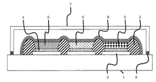
図1は本発明の実施の形態による有機ELディスプレイパネルの構造を示す断面図である。
この有機ELディスプレイパネルにおける有機EL素子は基板上に形成される。この有機ELディスプレイパネルが基板側から光を取り出すポトムエミッション方式の有機EL素子とする場合には、基板として透明なものを使用する必要があるが、基板と反対側から光を取り出すトップエミッション方式の場合は、基板は透光性を有する必要はない。
基板1としては、ガラス基板やプラスチック製のフィルムまたはシートを用いることができる。プラスチック製のフィルムを用いれば、巻取りにより高分子EL素子の製造が可能となり、安価にディスプレイパネルを提供できる。また、その場合のプラスチックとしては、例えば、ポリエチレンテレフタレート、ポリプロピレン、シクロオレフィンポリマー、ポリアミド、ポリエーテルスルホン、ポリメタクリル酸メチル、ポリカーボネート等を用いることができる。また、これらのフィルムは水蒸気バリア性、酸素バリア性を示す酸化ケイ素といった金属酸化物、窒化ケイ素といった酸化窒化物やポリ塩化ビニリデン、ポリ塩化ビニル、エチレン−酢酸ビニル共重合体鹸化物からなるバリア層が必要に応じて設けられる。
Hereinafter, an example in which the embodiment of the present invention is applied to a passive matrix type organic EL display panel will be described. There are a passive matrix type and an active matrix type as a driving method of the organic EL element, but the organic EL element of the present invention can be applied to both a passive matrix type organic EL element and an active matrix type organic EL element. .
The passive matrix method is a method in which stripe-shaped electrodes are opposed to each other so as to be orthogonal to each other, and light is emitted at the intersection, whereas the active matrix method uses a so-called thin film transistor (TFT) substrate in which a transistor is formed for each pixel. Thus, the light is emitted independently for each pixel.
FIG. 1 is a sectional view showing the structure of an organic EL display panel according to an embodiment of the present invention.
The organic EL element in this organic EL display panel is formed on a substrate. When this organic EL display panel is an organic EL element of the pottom emission type that extracts light from the substrate side, it is necessary to use a transparent substrate, but the top emission method that extracts light from the opposite side of the substrate In this case, the substrate does not need to have translucency.
As the substrate 1, a glass substrate or a plastic film or sheet can be used. If a plastic film is used, a polymer EL element can be produced by winding, and a display panel can be provided at a low cost. In addition, as the plastic in that case, for example, polyethylene terephthalate, polypropylene, cycloolefin polymer, polyamide, polyethersulfone, polymethyl methacrylate, polycarbonate, or the like can be used. In addition, these films have a barrier layer made of a metal oxide such as silicon oxide that exhibits water vapor barrier property and oxygen barrier property, oxynitride such as silicon nitride, polyvinylidene chloride, polyvinyl chloride, saponified ethylene-vinyl acetate copolymer. Is provided as necessary.
また、基板1の上には陽極としてパターニングされた画素電極2が設けられる。画素電極2の材料としては、ITO(インジウム錫複合酸化物)、IZO(インジウム亜鉛複合酸化物)、酸化錫、酸化亜鉛、酸化インジウム、酸化アルミニウム複合酸化物等の透明電極材料が使用できる。なお、低抵抗であること、耐溶剤性があること、透明性があることなどからITOが好ましい。ITOはスパッタ法により基板上に形成されフォトリソグラフィ法によりパターニングされライン状の画素電極2となる。
そして、このライン状の画素電極2を形成後、隣接する画素電極の間に感光性材料を用いて、フォトリソグラフィ法により絶縁層3が形成される。絶縁層3は、画素電極2上に発光領域を画定する。
A pixel electrode 2 patterned as an anode is provided on the substrate 1. As the material of the pixel electrode 2, transparent electrode materials such as ITO (indium tin composite oxide), IZO (indium zinc composite oxide), tin oxide, zinc oxide, indium oxide, and aluminum oxide composite oxide can be used. ITO is preferred because of its low resistance, solvent resistance, transparency, and the like. ITO is formed on the substrate by sputtering and patterned by photolithography to form line-shaped pixel electrodes 2.
Then, after the line-shaped pixel electrode 2 is formed, an insulating layer 3 is formed by a photolithography method using a photosensitive material between adjacent pixel electrodes. The insulating layer 3 defines a light emitting region on the pixel electrode 2.
本実施の形態における絶縁層3は、厚みが0.5μmから5.0μmの範囲にあることが望ましい。また、絶縁層を隣接する画素電極間に設けることによって、各画素電極上に印刷された正孔輸送インキの広がりを抑え、ディスプレイ化した際に正孔輸送層が絶縁層上にあることによるリーク電流の発生を防ぐことができる。なお、絶縁層が低すぎるとインキの広がりを防止できずに絶縁層上に正孔輸送層が形成されることとなる。 The insulating layer 3 in the present embodiment desirably has a thickness in the range of 0.5 μm to 5.0 μm. In addition, by providing an insulating layer between adjacent pixel electrodes, the spread of the hole transport ink printed on each pixel electrode is suppressed, and leaks due to the presence of the hole transport layer on the insulating layer when a display is made. Generation of current can be prevented. If the insulating layer is too low, ink spreading cannot be prevented and a hole transport layer is formed on the insulating layer.
また、例えばパッシブマトリックスタイプの有機ELディスプレイパネルにおいて、画素電極の間に絶縁層を設けた場合、絶縁層を直交して陰極層を形成することになる。このように絶縁層をまたぐ形で陰極層を形成する場合、絶縁層が高すぎると陰極層の断線が起こってしまい表示不良となる。絶縁層の高さが5.0μmを超えると陰極の断線が起きやすくなってしまう。 For example, in an organic EL display panel of a passive matrix type, when an insulating layer is provided between pixel electrodes, a cathode layer is formed with the insulating layers orthogonal to each other. When the cathode layer is formed so as to straddle the insulating layer in this way, if the insulating layer is too high, the cathode layer is disconnected, resulting in a display defect. When the height of the insulating layer exceeds 5.0 μm, disconnection of the cathode tends to occur.
また、絶縁層を形成する感光性材料としてはポジ型レジスト、ネガ型レジストのどちらであってもよく、市販のもので構わないが、絶縁性を有する必要がある。なお、隔壁が十分な絶縁性を有さない場合には隔壁を通じて隣り合う画素電極に電流が流れてしまい表示不良が発生してしまう。具体的にはポリイミド系、アクリル樹脂系、ノボラック樹脂系、フルオレン系といったものが挙げられるが、これに限定するものではない。また、有機EL素子の表示品位を上げる目的で、光遮光性の材料を感光性材料に含有させても良い。 The photosensitive material for forming the insulating layer may be either a positive resist or a negative resist, and may be a commercially available one, but it must have insulating properties. Note that if the partition does not have sufficient insulation, a current flows to the adjacent pixel electrode through the partition and a display defect occurs. Specific examples thereof include polyimide, acrylic resin, novolac resin, and fluorene, but are not limited thereto. Further, for the purpose of improving the display quality of the organic EL element, a light shielding material may be included in the photosensitive material.
また、絶縁層3を形成する感光性樹脂はスピンコーター、バーコーター、ロールコーター、ダイコーター、グラビアコーター等の塗布方法を用いて塗布され、フォトリソグラフィ法によりパターニングされる。また、感光性樹脂を用いずにグラビアオフセット印刷法、反転印刷法、フレキソ印刷法等を用いて絶縁層を形成してもよい。 The photosensitive resin for forming the insulating layer 3 is applied using a coating method such as a spin coater, bar coater, roll coater, die coater, gravure coater, and patterned by a photolithography method. Alternatively, the insulating layer may be formed using a gravure offset printing method, a reverse printing method, a flexographic printing method, or the like without using a photosensitive resin.
以上のようにして絶縁層3を形成した後、次に正孔輸送層4を形成する。正孔輸送層4を形成する正孔輸送材料としては、ポリアニリン誘導体、ポリチオフェン誘導体、ポリビニルカルバゾール(PVK)誘導体、ポリ(3,4―エチレンジオキシチオフェン)(PEDOT)等が挙げられる。これらの材料は溶媒に溶解または分散させ、正孔輸送材料インキとなり、本実施の形態による凸版印刷方法を用いて形成される。なお、形成される正孔輸送層の体積抵抗率は発光効率の点から1x10⁶Ω・cm以下のものが好ましい。
After forming the insulating layer 3 as described above, the
また、正孔輸送材料を溶解または分散させる溶媒としては、例えば、トルエン、キシレン、アセトン、メチルエチルケトン、メチルイソブチルケトン、シクロヘキサノン、メタノール、エタノール、イソプロパノール、エチレングリコール、プロピレングリコール、ポリエチレングリコール、グリセリン、酢酸エチル、酢酸ブチル、酢酸イソプロピル、酢酸メチルセロソルブ、酢酸エチルセロソルブ、メチルセロソルブ、エチルセロソルブ、ブチルセロソルブ、乳酸エチル、エチレングリコールジエチルエーテル、1−プロパノール、メトキシプロパノール、エトキシプロパノール、水等の単独またはこれらの混合溶媒などが挙げられる。また、必要に応じて、界面活性剤、酸化防止剤、粘度調整剤、紫外線吸収剤等が添加されていても良い。 Examples of the solvent for dissolving or dispersing the hole transport material include toluene, xylene, acetone, methyl ethyl ketone, methyl isobutyl ketone, cyclohexanone, methanol, ethanol, isopropanol, ethylene glycol, propylene glycol, polyethylene glycol, glycerin, and ethyl acetate. , Butyl acetate, isopropyl acetate, methyl cellosolve, ethyl cellosolve, methyl cellosolve, ethyl cellosolve, butyl cellosolve, ethyl lactate, ethylene glycol diethyl ether, 1-propanol, methoxypropanol, ethoxypropanol, water, etc. Etc. Moreover, surfactant, antioxidant, a viscosity modifier, a ultraviolet absorber, etc. may be added as needed.
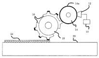
図2は正孔輸送材料からなる正孔輸送インキを、画素電極、絶縁層が形成された被印刷基板上にパターン印刷する際の凸版印刷装置の概略を示している。
図示のように、本装置は、インクタンク10と、インキチャンバー12と、アニロックスロール14と、凸版が設けられた版16がマウントされた版胴18を有している。インクタンク10には溶媒で希釈された正孔輸送インキが収容されており、インキチャンバー12にはインクタンク10より正孔輸送インキが送り込まれるようになっている。アニロックスロール14はインキチャンバー12のインキ供給部に対して回転可能に支持されている。
FIG. 2 shows an outline of a relief printing apparatus when pattern printing is performed on a substrate to be printed on which a pixel electrode and an insulating layer are formed using a hole transport ink made of a hole transport material.
As shown in the figure, the apparatus includes an
アニロックスロール14の回転に伴い、アニロックスロール表面に供給された正孔輸送インキのインキ層14aは均一な膜厚に形成される。このインキ層はアニロックスロールに近接して回転駆動される版胴18にマウントされた版16の凸部に転移する。
平台20には、画素電極および絶縁層が形成された被印刷基板24が版16の凸部による印刷位置にまで図示しない搬送手段によって搬送されるようになっている。そして、版16の凸部にあるインキは、本発明の所定の半乾燥に施された後、被印刷基板24に対して印刷され、必要に応じて乾燥工程を経て被印刷基板上に正孔輸送層が形成される。
As the
On the flat table 20, the substrate to be printed 24 on which the pixel electrode and the insulating layer are formed is transported to a printing position by the convex portion of the
なお、本例では凸版に使用した感光性樹脂凸版は水現像タイプのものを使用した。感光性樹脂版には、露光した樹脂版を現像する際に用いる現像液が有機溶剤である溶剤現像タイプのものと現像液が水である水現像タイプのものがある。一般に溶剤現像タイプのものは水系のインキに耐性を示し、水現像タイプのものは有機溶剤系のインキに耐性を示す傾向があるが、この限りではなく、正孔輸送インキに耐性を持ったものであれば、いずれの樹脂凸版も用いることができる。 In this example, the photosensitive resin relief plate used for the relief plate was a water development type. The photosensitive resin plate includes a solvent development type in which the developer used when developing the exposed resin plate is an organic solvent and a water development type in which the developer is water. In general, solvent development type is resistant to water-based ink, and water development type tends to be resistant to organic solvent-based ink. Any resin relief can be used.
また凸版の凸部と凹部、つまりインキが転移されない部分の深さの差は40μm以上であることが好ましい。これより凸部と凹部との差が小さいと、印刷条件によっては凸部だけでなく、凹部までも基板に接触してしまい、余計な部分にインキが転写してしまいリーク等の不具合が発生するためである。 Further, it is preferable that the difference in depth between the convex portion and the concave portion of the relief printing, that is, the portion where the ink is not transferred is 40 μm or more. If the difference between the convex part and the concave part is smaller than this, depending on the printing conditions, not only the convex part but also the concave part comes into contact with the substrate, and ink is transferred to the extra part, causing problems such as leakage. Because.
次に、樹脂凸版の硬度は45〜90度(ショアA)、18〜75度(ショアD)であることが好ましい。硬度が45度未満(ショアA)であると、印圧に対するマージンが狭く画線がよれたりつぶれたりしてしまい、均一なパターン形成をすることが非常に難しくなってしまうためである。また、75度(ショアD)より大きい場合では、パターン形成に適切な印圧が高くなりすぎ、基板や絶縁層に負荷がかかりすぎ、ワレやひずみ、キズを生じてしまう危険があるからである。 Next, the hardness of the resin relief printing plate is preferably 45 to 90 degrees (Shore A) and 18 to 75 degrees (Shore D). This is because if the hardness is less than 45 degrees (Shore A), the margin for the printing pressure is narrow and the image line is twisted or crushed, making it very difficult to form a uniform pattern. Further, when the angle is greater than 75 degrees (Shore D), the printing pressure appropriate for pattern formation becomes too high, and the substrate and the insulating layer are overloaded, and there is a risk of cracking, distortion, and scratches. .
また、相対湿度40〜50%、温度23〜26℃の条件下において、正孔輸送インキの粘度は10〜30mPa・sであることが好ましい。これは、本実施の形態で用いる凸版印刷法ではアニロックスから凸版上へのインキの転写が最初に行われるが、30mPa・sを超える粘度ではアニロックスから凸版上へインキが転写した後、凸版上で十分インキがレベリングせず、ムラの原因になる。 Moreover, it is preferable that the viscosity of hole transport ink is 10-30 mPa * s on the conditions of relative humidity 40-50% and temperature 23-26 degreeC. In the relief printing method used in the present embodiment, the ink is first transferred from the anilox to the relief plate. However, at a viscosity exceeding 30 mPa · s, the ink is transferred from the anilox to the relief plate, and then on the relief plate. Insufficient ink leveling causes unevenness.
また、上記相対湿度および温度条件下において、正孔輸送インキの固形分濃度としては0.5〜4.0重量%であることが好ましい。これは、本実施の形態で用いる正孔輸送インキでは、4.0重量%超の濃度ではインキの安定性が悪くなり、インキ凝集や正孔輸送層のムラの原因になるからである。 Moreover, it is preferable that it is 0.5 to 4.0 weight% as solid content concentration of hole transport ink on the said relative humidity and temperature conditions. This is because the hole transport ink used in the present embodiment is not stable when the concentration exceeds 4.0% by weight, and causes ink aggregation and hole transport layer unevenness.
また、上記相対湿度および温度条件下において、正孔輸送インキの蒸気圧としては0.1〜20kPaであることが好ましい。これは、本実施の形態で用いる凸版印刷法ではアニロックスから凸版上へのインキの転写が最初に行われるが、20kPa超の蒸気圧ではアニロックスから凸版上へインキが転写した後、凸版上でインキの乾燥が速すぎて、転写不良を起こし、ムラの原因になるからである。 Further, the vapor pressure of the hole transport ink is preferably 0.1 to 20 kPa under the above relative humidity and temperature conditions. In the relief printing method used in this embodiment, the ink is first transferred from the anilox to the relief plate, but after the ink is transferred from the anilox to the relief plate at a vapor pressure of more than 20 kPa, the ink is transferred onto the relief plate. This is because the drying of the toner is too fast, causing transfer defects and causing unevenness.
また、半乾燥後における正孔輸送インキの濃度が5〜30重量%、粘度が30〜100mPa・sであることが好ましい。30mP・s未満の粘度では、絶縁層へのぬれ上がりを抑えることができず、絶縁層と画素電極が接する縁部において厚膜化を引き起こし、発光ムラや輝度低下の原因になる。 Moreover, it is preferable that the density | concentration of the hole transport ink after semi-drying is 5 to 30 weight%, and a viscosity is 30-100 mPa * s. When the viscosity is less than 30 mP · s, wetting to the insulating layer cannot be suppressed, and the film is thickened at the edge where the insulating layer and the pixel electrode are in contact with each other, resulting in light emission unevenness and luminance reduction.
次に、以上のような正孔輸送層4の形成後、有機発光層5を形成する。有機発光層は電流を通すことにより発光する層であり、有機発光層を形成する有機発光材料は、例えば、クマリン系、ペリレン系、ピラン系、アンスロン系、ポルフィレン系、キナクリドン系、N,N’−ジアルキル置換キナクリドン系、ナフタルイミド系、N,N’−ジアリール置換ピロロピロール系、イリジウム錯体系等の発光性色素をポリスチレン、ポリメチルメタクリレート、ポリビニルカルバゾール等の高分子中に分散させたものや、ポリアリーレン系、ポリアリーレンビニレン系やポリフルオレン系の高分子材料が挙げられる。
Next, after the formation of the
これらの有機発光材料は溶媒に溶解または安定に分散させ有機発光インキとなる。有機発光材料を溶解または分散する溶媒としては、トルエン、キシレン、アセトン、アニソール、メチルエチルケトン、メチルイソブチルケトン、シクロヘキサノン等の単独またはこれらの混合溶媒が挙げられる。中でも、トルエン、キシレン、アニソールといった芳香族有機溶剤が有機発光材料の溶解性の面から好適である。また、有機発光インキには、必要に応じて、界面活性剤、酸化防止剤、粘度調整剤、紫外線吸収剤等が添加されても良い。 These organic light emitting materials are dissolved or stably dispersed in a solvent to form an organic light emitting ink. Examples of the solvent for dissolving or dispersing the organic light-emitting material include toluene, xylene, acetone, anisole, methyl ethyl ketone, methyl isobutyl ketone, cyclohexanone, or a mixed solvent thereof. Among these, aromatic organic solvents such as toluene, xylene, and anisole are preferable from the viewpoint of solubility of the organic light emitting material. Moreover, surfactant, antioxidant, a viscosity modifier, a ultraviolet absorber, etc. may be added to organic luminescent ink as needed.
有機発光層5の形成方法としては、凸版印刷法を用いる場合は、有機発光インキに適した樹脂凸版を使用することができ、中でも水現像タイプの感光性樹脂凸版が好適である。
As a method for forming the organic
有機発光インキを印刷する際の印刷方法は、正孔輸送層印刷と同様に行うことができる。 The printing method for printing the organic light emitting ink can be performed in the same manner as the hole transport layer printing.
次に、以上のような有機発光層5の形成後、対向電極6を画素電極のラインパターンと直交するラインパターンで形成する。この対向電極6の材料としては、有機発光層の発光特性に応じたものを使用でき、例えば、リチウム、マグネシウム、カルシウム、イッテルビウム、アルミニウムなどの金属単体やこれらと金、銀などの安定な金属との合金などが挙げられる。また、インジウム、亜鉛、錫などの導電性酸化物を用いることもできる。対向電極の形成方法としてはマスクを用いた真空蒸着法による形成方法が挙げられる。
Next, after forming the organic
なお、本実施の形態の有機EL素子は、陽極である画素電極と陰極である対向電極の間に陽極層側から正孔輸送層と有機発光媒体層を積層した構成であるが、陽極層と陰極層の間において正孔輸送層、有機発光媒体層以外に正孔ブロック層、電子輸送層、電子注入層といった層を必要に応じ選択した積層構造をとることができる。また、これらの層を形成する際にも本発明の方法を使用できる。 Note that the organic EL element of the present embodiment has a structure in which a hole transport layer and an organic light emitting medium layer are stacked from the anode layer side between a pixel electrode as an anode and a counter electrode as a cathode. Between the cathode layers, in addition to the hole transport layer and the organic light emitting medium layer, a layered structure in which layers such as a hole block layer, an electron transport layer, and an electron injection layer are selected as necessary can be employed. The method of the present invention can also be used when forming these layers.
最後に、これらの有機EL素子を、外部の酸素や水分から保護するために、ガラスキャップ7と接着剤8を用いて密閉封止し、有機ELディスプレイパネルを得ることができる。また、基板が可撓性を有する場合には、封止剤と可撓性フィルムを用いて封止を行っても良い。
Finally, in order to protect these organic EL elements from external oxygen and moisture, the organic EL display panel can be obtained by hermetically sealing with a
以下、本発明を実施例および比較例によりさらに説明するが、本発明は下記例に制限されるものではない。 EXAMPLES Hereinafter, although an Example and a comparative example further demonstrate this invention, this invention is not restrict | limited to the following example.
実施例1
まず、300mm角のガラス基板の上に、スパッタ法を用いてITO(インジウム-錫酸化物)薄膜を形成し、フォトリソグラフィ法と酸溶液によるエッチングでITO膜をパターニングして、対角5インチサイズのディスプレイが2面取れるように画素電極を形成した。ディスプレイ1面当たりの画素電極のラインパターンは、線幅40μm、スペース20μmでラインが1950ライン形成されるパターンとした。
Example 1
First, an ITO (indium-tin oxide) thin film is formed on a 300 mm square glass substrate by sputtering, and the ITO film is patterned by photolithography and etching with an acid solution to obtain a 5 inch diagonal size. Pixel electrodes were formed so that two displays could be taken. The line pattern of the pixel electrode per display surface was a pattern in which 1950 lines were formed with a line width of 40 μm and a space of 20 μm.
次に絶縁層を以下のように形成した。まず、画素電極を形成したガラス基板上にアクリル系のフォトレジスト材料を全面スピンコートした。スピンコートの条件を150rpmで5秒間回転させた後、500rpmで20秒間回転させ1回コーティングとし、絶縁層の高さを1.5μmとした。全面に塗布したフォトレジスト材料に対し、フォトリソグラフィ法により画素電極の間にラインパターンを有する絶縁層を形成した。 Next, an insulating layer was formed as follows. First, an acrylic photoresist material was spin-coated on the entire surface of a glass substrate on which pixel electrodes were formed. The spin coating condition was rotated at 150 rpm for 5 seconds, and then rotated at 500 rpm for 20 seconds to make a single coating, and the height of the insulating layer was 1.5 μm. An insulating layer having a line pattern between pixel electrodes was formed on the photoresist material applied to the entire surface by photolithography.
次に、正孔輸送インキとしてPEDOT溶液であるバイトロンCH―8000を用いて調液しインキの固形分濃度1.5%、相対湿度45%、温度25℃の条件下、粘度15mPa・s、蒸気圧1.1kPaのインキを用意した。インキ及び版を用いて相対湿度45%、温度25℃の条件下において、アニロックスロールからうけとったインキを版の上で15秒間の半乾燥する時間を設け、凸版印刷法にて絶縁層間に正孔輸送層を形成した。
なお、半乾燥後の正孔輸送インキの固形分濃度は7.5重量%、粘度は45mPa.sであった。
印刷には180線/インチのアニロックスロールを使用し、印刷後、200°C、30分大気中で乾燥を行い正孔輸送層を形成した。このときの膜厚は50nmとなった。そして、形成された正孔輸送層に対し、パターニング状態の確認を行った。
Next, it was prepared by using PEDOT solution Vitron CH-8000 as a hole transport ink, and the viscosity of the ink was 15 mPa · s, vapor under conditions of solid content concentration of ink 1.5%, relative humidity 45%, temperature 25 ° C. An ink having a pressure of 1.1 kPa was prepared. The ink received from the anilox roll was dried for 15 seconds on the plate under conditions of 45% relative humidity and a temperature of 25 ° C. using ink and plate. A transport layer was formed.
The solid content concentration of the hole transport ink after semi-drying was 7.5% by weight and the viscosity was 45 mPa.s. s.
A 180 line / inch anilox roll was used for printing, and after printing, drying was performed in the atmosphere at 200 ° C. for 30 minutes to form a hole transport layer. The film thickness at this time was 50 nm. And the patterning state was confirmed with respect to the formed positive hole transport layer.
次に、有機発光材料であるポリフェニレンビニレン誘導体を濃度1%になるようにトルエンに溶解させた有機発光インキを用い、絶縁層に挟まれた画素電極の真上にそのラインパターンにあわせて有機発光層を凸版印刷法で印刷を行った。このとき150線/インチのアニロックスロール及び水現像タイプの感光性樹脂版を使用した。この結果、印刷、乾燥後の有機発光層の膜厚は80nmとなった。 Next, organic light-emitting ink in which polyphenylene vinylene derivative, an organic light-emitting material, is dissolved in toluene to a concentration of 1% is used, and organic light emission is performed in line with the line pattern directly above the pixel electrode sandwiched between insulating layers. The layer was printed by letterpress printing. At this time, an anilox roll of 150 lines / inch and a photosensitive resin plate of water development type were used. As a result, the film thickness of the organic light emitting layer after printing and drying was 80 nm.
その上にCa、Alからなる陰極層を画素電極のラインパターンと直交するようなラインパターンで抵抗加熱蒸着法によりマスク蒸着して形成した。最後にこれらの有機EL素子を、外部の酸素や水分から保護するために、ガラスキャップと接着剤を用いて密閉封止し、有機ELディスプレイパネルを作製した。
これにより得られた有機ELディスプレイパネルの表示部の周辺部には各画素電極に接続されている陽極側の取り出し電極と、陰極側の取り出し電極があり、これらを電源に接続することにより、得られた有機ELディスプレイパネルの点灯表示確認を行い、発光状態のチェックを行った。
A cathode layer made of Ca and Al was formed thereon by mask vapor deposition using a resistance heating vapor deposition method in a line pattern orthogonal to the pixel electrode line pattern. Finally, in order to protect these organic EL elements from external oxygen and moisture, they were hermetically sealed using a glass cap and an adhesive to produce an organic EL display panel.
In the periphery of the display part of the organic EL display panel obtained in this way, there are an extraction electrode on the anode side connected to each pixel electrode and an extraction electrode on the cathode side, which are obtained by connecting them to a power source. The lighting display of the obtained organic EL display panel was confirmed, and the light emission state was checked.
実施例2
正孔輸送インキの粘度150mPa・sとした以外は実施例1と同様とした。
Example 2
The same procedure as in Example 1 was performed except that the viscosity of the hole transport ink was 150 mPa · s.
実施例3
正孔輸送インキの蒸気圧が0.05kPaとした以外は実施例1と同様とした。
Example 3
The same as Example 1 except that the vapor pressure of the hole transport ink was 0.05 kPa.
実施例4
半乾燥する時間を2秒間とした以外は実施例1と同様とした。
Example 4
Example 1 was repeated except that the semi-drying time was 2 seconds.
比較例1
半乾燥時間を設けない以外は実施例1と同様に行った。
Comparative Example 1
It carried out like Example 1 except not providing a half-dry time.
以上のような実施例1〜4及び比較例1での正孔輸送層のラインパターン形状の評価結果と、作製した有機ELディスプレイの表示状態の評価結果を下記の表1に示す。 The evaluation results of the line pattern shape of the hole transport layer in Examples 1 to 4 and Comparative Example 1 as described above and the evaluation results of the display state of the produced organic EL display are shown in Table 1 below.
[表1]
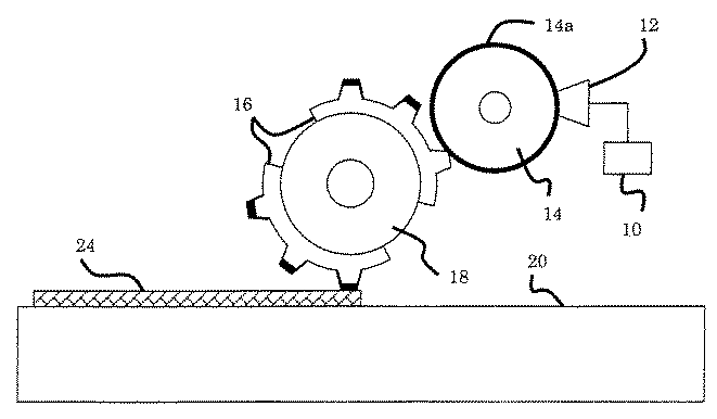
表1の結果から分かるように、比較例に比べて本発明の実施例で良好な結果が得られることが分かる。 As can be seen from the results in Table 1, it can be seen that better results are obtained in the examples of the present invention than in the comparative examples.
本発明の有機EL素子は、発光ムラや輝度低下をなくした均一性の良い表示を行うことができるので、有機ELディスプレイパネルに有用である。 The organic EL device of the present invention is useful for an organic EL display panel because it can perform display with good uniformity without causing unevenness of light emission and lowering of luminance.
1……基板、2……画素電極、3……絶縁層、4……正孔輸送層、5……有機発光層、6……対向電極、7……ガラスキャップ、8……接着剤、10……インクタンク、12……インキチャンバー、14……アニロックスロール、14a……インキ層、16……版、18……版胴、20……平台、24……被印刷基板。
DESCRIPTION OF SYMBOLS 1 ... Substrate, 2 ... Pixel electrode, 3 ... Insulating layer, 4 ... Hole transport layer, 5 ... Organic light emitting layer, 6 ... Counter electrode, 7 ... Glass cap, 8 ... Adhesive, DESCRIPTION OF
Claims (5)
前記発光領域内に、正孔輸送材料を溶媒に溶解または分散させた正孔輸送インキを凸版印刷法により凸版の凸部から前記絶縁層の間にある画素電極に印刷して正孔輸送層を形成する工程を備え、その際、前記凸版の上で正孔輸送インキが半乾燥する時間を設けることで、前記正孔輸送インキの濃度と粘度を増加させることを特徴とする有機エレクトロルミネッセンス素子の製造方法。 A pixel electrode; an insulating layer defining a light emitting region on the pixel electrode; an organic light emitting medium layer including at least two layers of a hole transport layer and an organic light emitting medium layer stacked on the light emitting region; and the organic light emitting medium A method for producing an organic electroluminescent element comprising a counter electrode facing the pixel electrode through a layer,
In the light emitting region, a hole transporting layer in which a hole transporting material is dissolved or dispersed in a solvent is printed on a pixel electrode between a convex portion of the relief printing and the insulating layer by a relief printing method. An organic electroluminescence device comprising: a step of forming, wherein at that time, a time for the semi-drying of the hole transport ink on the relief printing plate is provided, thereby increasing the concentration and viscosity of the hole transport ink. Production method.
Priority Applications (1)
| Application Number | Priority Date | Filing Date | Title |
|---|---|---|---|
| JP2007039404A JP4998008B2 (en) | 2007-02-20 | 2007-02-20 | Organic electroluminescence device and method for manufacturing the same |
Applications Claiming Priority (1)
| Application Number | Priority Date | Filing Date | Title |
|---|---|---|---|
| JP2007039404A JP4998008B2 (en) | 2007-02-20 | 2007-02-20 | Organic electroluminescence device and method for manufacturing the same |
Publications (3)
| Publication Number | Publication Date |
|---|---|
| JP2008204792A true JP2008204792A (en) | 2008-09-04 |
| JP2008204792A5 JP2008204792A5 (en) | 2010-02-18 |
| JP4998008B2 JP4998008B2 (en) | 2012-08-15 |
Family
ID=39782067
Family Applications (1)
| Application Number | Title | Priority Date | Filing Date |
|---|---|---|---|
| JP2007039404A Expired - Fee Related JP4998008B2 (en) | 2007-02-20 | 2007-02-20 | Organic electroluminescence device and method for manufacturing the same |
Country Status (1)
| Country | Link |
|---|---|
| JP (1) | JP4998008B2 (en) |
Cited By (3)
| Publication number | Priority date | Publication date | Assignee | Title |
|---|---|---|---|---|
| WO2011122461A1 (en) * | 2010-03-29 | 2011-10-06 | 住友化学株式会社 | Method of manufacturing light-emitting apparatus |
| JP2011204504A (en) * | 2010-03-26 | 2011-10-13 | Toppan Printing Co Ltd | Manufacturing method of organic el display device, and organic el display device |
| CN110168764A (en) * | 2017-01-30 | 2019-08-23 | 默克专利有限公司 | The method for forming the organic element of electronic device |
Citations (3)
| Publication number | Priority date | Publication date | Assignee | Title |
|---|---|---|---|---|
| JP2004319094A (en) * | 2003-04-10 | 2004-11-11 | Sumitomo Rubber Ind Ltd | Method of forming front electrode for plasma display panel |
| JP2006286309A (en) * | 2005-03-31 | 2006-10-19 | Toppan Printing Co Ltd | Organic EL display device and manufacturing method thereof |
| JP2006318781A (en) * | 2005-05-13 | 2006-11-24 | Toppan Printing Co Ltd | Ink for letterpress printing and organic electroluminescence element |
-
2007
- 2007-02-20 JP JP2007039404A patent/JP4998008B2/en not_active Expired - Fee Related
Patent Citations (3)
| Publication number | Priority date | Publication date | Assignee | Title |
|---|---|---|---|---|
| JP2004319094A (en) * | 2003-04-10 | 2004-11-11 | Sumitomo Rubber Ind Ltd | Method of forming front electrode for plasma display panel |
| JP2006286309A (en) * | 2005-03-31 | 2006-10-19 | Toppan Printing Co Ltd | Organic EL display device and manufacturing method thereof |
| JP2006318781A (en) * | 2005-05-13 | 2006-11-24 | Toppan Printing Co Ltd | Ink for letterpress printing and organic electroluminescence element |
Cited By (4)
| Publication number | Priority date | Publication date | Assignee | Title |
|---|---|---|---|---|
| JP2011204504A (en) * | 2010-03-26 | 2011-10-13 | Toppan Printing Co Ltd | Manufacturing method of organic el display device, and organic el display device |
| WO2011122461A1 (en) * | 2010-03-29 | 2011-10-06 | 住友化学株式会社 | Method of manufacturing light-emitting apparatus |
| CN110168764A (en) * | 2017-01-30 | 2019-08-23 | 默克专利有限公司 | The method for forming the organic element of electronic device |
| CN110168764B (en) * | 2017-01-30 | 2023-04-04 | 默克专利有限公司 | Method of forming organic elements of electronic devices |
Also Published As
| Publication number | Publication date |
|---|---|
| JP4998008B2 (en) | 2012-08-15 |
Similar Documents
| Publication | Publication Date | Title |
|---|---|---|
| JP2008140724A (en) | Method for manufacturing organic EL element and organic EL element | |
| JP5092485B2 (en) | Organic electroluminescence display and manufacturing method thereof | |
| JP2009004347A (en) | Manufacturing method of organic EL display element and organic EL display element | |
| JP2007299616A (en) | Method for manufacturing organic EL element and organic EL element | |
| JP2006286309A (en) | Organic EL display device and manufacturing method thereof | |
| JP2007095343A (en) | Method for producing printed matter and printed matter | |
| CN103120022B (en) | Printing relief printing plate and use the manufacture method of organic EL element of this printing relief printing plate | |
| JP4882508B2 (en) | Method for manufacturing organic electroluminescence device | |
| JP2009135085A (en) | Organic EL display and manufacturing method thereof | |
| JP4706845B2 (en) | Manufacturing method of organic EL element | |
| JP4998008B2 (en) | Organic electroluminescence device and method for manufacturing the same | |
| JP2012204202A (en) | Organic electroluminescent panel and method for manufacturing the same | |
| JP5218172B2 (en) | ORGANIC EL LIGHT EMITTING ELEMENT AND MANUFACTURING METHOD THEREOF | |
| JP4978133B2 (en) | Manufacturing method of organic EL element | |
| JP4747637B2 (en) | Manufacturing method of organic EL display panel | |
| JP2008077912A (en) | Method for manufacturing organic electroluminescence device | |
| JP2008186766A (en) | Method for manufacturing organic electroluminescence device | |
| JP2008140579A (en) | ORGANIC EL ELEMENT AND ITS MANUFACTURING METHOD | |
| JP2007200699A (en) | Organic EL device and manufacturing method thereof | |
| JP2008282952A (en) | Organic EL device and manufacturing method thereof | |
| JP2008140588A (en) | ORGANIC EL ELEMENT AND ITS MANUFACTURING METHOD | |
| JP2014067543A (en) | Organic el element and method for manufacturing organic el element | |
| JP2008077958A (en) | Manufacturing method of organic EL element | |
| JP2006286241A (en) | Organic EL display panel and manufacturing method thereof | |
| JP2015185531A (en) | Organic electroluminescence device and method for manufacturing the same |
Legal Events
| Date | Code | Title | Description |
|---|---|---|---|
| A521 | Request for written amendment filed |
Free format text: JAPANESE INTERMEDIATE CODE: A523 Effective date: 20091228 |
|
| A621 | Written request for application examination |
Free format text: JAPANESE INTERMEDIATE CODE: A621 Effective date: 20100126 |
|
| A521 | Request for written amendment filed |
Free format text: JAPANESE INTERMEDIATE CODE: A523 Effective date: 20110223 |
|
| A977 | Report on retrieval |
Free format text: JAPANESE INTERMEDIATE CODE: A971007 Effective date: 20110922 |
|
| A131 | Notification of reasons for refusal |
Free format text: JAPANESE INTERMEDIATE CODE: A131 Effective date: 20110929 |
|
| A521 | Request for written amendment filed |
Free format text: JAPANESE INTERMEDIATE CODE: A523 Effective date: 20111124 |
|
| TRDD | Decision of grant or rejection written | ||
| A01 | Written decision to grant a patent or to grant a registration (utility model) |
Free format text: JAPANESE INTERMEDIATE CODE: A01 Effective date: 20120417 |
|
| A01 | Written decision to grant a patent or to grant a registration (utility model) |
Free format text: JAPANESE INTERMEDIATE CODE: A01 |
|
| A61 | First payment of annual fees (during grant procedure) |
Free format text: JAPANESE INTERMEDIATE CODE: A61 Effective date: 20120430 |
|
| R150 | Certificate of patent or registration of utility model |
Free format text: JAPANESE INTERMEDIATE CODE: R150 |
|
| FPAY | Renewal fee payment (event date is renewal date of database) |
Free format text: PAYMENT UNTIL: 20150525 Year of fee payment: 3 |
|
| LAPS | Cancellation because of no payment of annual fees |