JP2008511994A - 集積回路の製造における複数の深さを有するstiトレンチ - Google Patents
集積回路の製造における複数の深さを有するstiトレンチ Download PDFInfo
- Publication number
- JP2008511994A JP2008511994A JP2007530152A JP2007530152A JP2008511994A JP 2008511994 A JP2008511994 A JP 2008511994A JP 2007530152 A JP2007530152 A JP 2007530152A JP 2007530152 A JP2007530152 A JP 2007530152A JP 2008511994 A JP2008511994 A JP 2008511994A
- Authority
- JP
- Japan
- Prior art keywords
- groove
- substrate
- forming
- dielectric layer
- region
- Prior art date
- Legal status (The legal status is an assumption and is not a legal conclusion. Google has not performed a legal analysis and makes no representation as to the accuracy of the status listed.)
- Pending
Links
Images
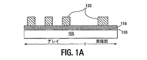

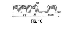


Classifications
-
- H—ELECTRICITY
- H10—SEMICONDUCTOR DEVICES; ELECTRIC SOLID-STATE DEVICES NOT OTHERWISE PROVIDED FOR
- H10W—GENERIC PACKAGES, INTERCONNECTIONS, CONNECTORS OR OTHER CONSTRUCTIONAL DETAILS OF DEVICES COVERED BY CLASS H10
- H10W10/00—Isolation regions in semiconductor bodies between components of integrated devices
- H10W10/10—Isolation regions comprising dielectric materials
- H10W10/17—Isolation regions comprising dielectric materials formed using trench refilling with dielectric materials, e.g. shallow trench isolations
-
- H—ELECTRICITY
- H10—SEMICONDUCTOR DEVICES; ELECTRIC SOLID-STATE DEVICES NOT OTHERWISE PROVIDED FOR
- H10P—GENERIC PROCESSES OR APPARATUS FOR THE MANUFACTURE OR TREATMENT OF DEVICES COVERED BY CLASS H10
- H10P90/00—Preparation of wafers not covered by a single main group of this subclass, e.g. wafer reinforcement
- H10P90/19—Preparing inhomogeneous wafers
- H10P90/1904—Preparing vertically inhomogeneous wafers
- H10P90/1906—Preparing SOI wafers
- H10P90/1922—Preparing SOI wafers using silicon etch back techniques, e.g. BESOI or ELTRAN
-
- H—ELECTRICITY
- H10—SEMICONDUCTOR DEVICES; ELECTRIC SOLID-STATE DEVICES NOT OTHERWISE PROVIDED FOR
- H10P—GENERIC PROCESSES OR APPARATUS FOR THE MANUFACTURE OR TREATMENT OF DEVICES COVERED BY CLASS H10
- H10P95/00—Generic processes or apparatus for manufacture or treatments not covered by the other groups of this subclass
- H10P95/06—Planarisation of inorganic insulating materials
-
- H—ELECTRICITY
- H10—SEMICONDUCTOR DEVICES; ELECTRIC SOLID-STATE DEVICES NOT OTHERWISE PROVIDED FOR
- H10W—GENERIC PACKAGES, INTERCONNECTIONS, CONNECTORS OR OTHER CONSTRUCTIONAL DETAILS OF DEVICES COVERED BY CLASS H10
- H10W10/00—Isolation regions in semiconductor bodies between components of integrated devices
- H10W10/01—Manufacture or treatment
- H10W10/011—Manufacture or treatment of isolation regions comprising dielectric materials
- H10W10/014—Manufacture or treatment of isolation regions comprising dielectric materials using trench refilling with dielectric materials, e.g. shallow trench isolations
- H10W10/0143—Manufacture or treatment of isolation regions comprising dielectric materials using trench refilling with dielectric materials, e.g. shallow trench isolations comprising concurrently refilling multiple trenches having different shapes or dimensions
Landscapes
- Element Separation (AREA)
- Semiconductor Memories (AREA)
- Non-Volatile Memory (AREA)
- Metal-Oxide And Bipolar Metal-Oxide Semiconductor Integrated Circuits (AREA)
Applications Claiming Priority (2)
| Application Number | Priority Date | Filing Date | Title |
|---|---|---|---|
| US10/931,946 US7354812B2 (en) | 2004-09-01 | 2004-09-01 | Multiple-depth STI trenches in integrated circuit fabrication |
| PCT/US2005/030377 WO2006028731A2 (fr) | 2004-09-01 | 2005-08-25 | Formation de tranchees sti multi-profondeur dans un circuit integre |
Publications (1)
| Publication Number | Publication Date |
|---|---|
| JP2008511994A true JP2008511994A (ja) | 2008-04-17 |
Family
ID=35219278
Family Applications (1)
| Application Number | Title | Priority Date | Filing Date |
|---|---|---|---|
| JP2007530152A Pending JP2008511994A (ja) | 2004-09-01 | 2005-08-25 | 集積回路の製造における複数の深さを有するstiトレンチ |
Country Status (6)
| Country | Link |
|---|---|
| US (2) | US7354812B2 (fr) |
| EP (1) | EP1794788A2 (fr) |
| JP (1) | JP2008511994A (fr) |
| KR (1) | KR100888370B1 (fr) |
| TW (1) | TWI276202B (fr) |
| WO (1) | WO2006028731A2 (fr) |
Cited By (1)
| Publication number | Priority date | Publication date | Assignee | Title |
|---|---|---|---|---|
| JP2012146693A (ja) * | 2011-01-06 | 2012-08-02 | Toshiba Corp | 半導体記憶装置及びその製造方法 |
Families Citing this family (42)
| Publication number | Priority date | Publication date | Assignee | Title |
|---|---|---|---|---|
| KR100602085B1 (ko) * | 2003-12-31 | 2006-07-14 | 동부일렉트로닉스 주식회사 | 반도체 소자 및 그의 제조 방법 |
| DE102004048536B4 (de) * | 2004-10-06 | 2008-09-18 | Clariant Produkte (Deutschland) Gmbh | Verwendung von Heißschmelzmassen in Straßenmarkierungen |
| US20070235783A9 (en) * | 2005-07-19 | 2007-10-11 | Micron Technology, Inc. | Semiconductor constructions, memory arrays, electronic systems, and methods of forming semiconductor constructions |
| KR100696382B1 (ko) * | 2005-08-01 | 2007-03-19 | 삼성전자주식회사 | 반도체 소자 및 그 제조방법 |
| US20070040235A1 (en) * | 2005-08-19 | 2007-02-22 | International Business Machines Corporation | Dual trench isolation for CMOS with hybrid orientations |
| US7375000B2 (en) * | 2005-08-22 | 2008-05-20 | International Business Machines Corporation | Discrete on-chip SOI resistors |
| US7772672B2 (en) | 2005-09-01 | 2010-08-10 | Micron Technology, Inc. | Semiconductor constructions |
| KR100660551B1 (ko) * | 2005-09-22 | 2006-12-22 | 삼성전자주식회사 | 불휘발성 메모리 소자 및 그 제조 방법 |
| US7279411B2 (en) * | 2005-11-15 | 2007-10-09 | International Business Machines Corporation | Process for forming a redundant structure |
| US20070132056A1 (en) * | 2005-12-09 | 2007-06-14 | Advanced Analogic Technologies, Inc. | Isolation structures for semiconductor integrated circuit substrates and methods of forming the same |
| US20070212874A1 (en) * | 2006-03-08 | 2007-09-13 | Micron Technology, Inc. | Method for filling shallow isolation trenches and other recesses during the formation of a semiconductor device and electronic systems including the semiconductor device |
| US7799694B2 (en) | 2006-04-11 | 2010-09-21 | Micron Technology, Inc. | Methods of forming semiconductor constructions |
| US20080113483A1 (en) * | 2006-11-15 | 2008-05-15 | Micron Technology, Inc. | Methods of etching a pattern layer to form staggered heights therein and intermediate semiconductor device structures |
| US7935610B2 (en) | 2006-11-28 | 2011-05-03 | Micron Technology, Inc. | Semiconductor device isolation structures |
| JP2009088134A (ja) * | 2007-09-28 | 2009-04-23 | Elpida Memory Inc | 半導体装置、半導体装置の製造方法並びにデータ処理システム |
| JP2009200107A (ja) * | 2008-02-19 | 2009-09-03 | Elpida Memory Inc | 半導体装置およびその製造方法 |
| JP2009295785A (ja) * | 2008-06-05 | 2009-12-17 | Toshiba Corp | 半導体装置の製造方法 |
| US8367515B2 (en) * | 2008-10-06 | 2013-02-05 | Taiwan Semiconductor Manufacturing Company, Ltd. | Hybrid shallow trench isolation for high-k metal gate device improvement |
| KR101045090B1 (ko) | 2008-11-13 | 2011-06-29 | 주식회사 하이닉스반도체 | 반도체 소자의 미세 패턴 형성방법 |
| JP5428394B2 (ja) * | 2009-03-04 | 2014-02-26 | ソニー株式会社 | 固体撮像装置とその製造方法、および撮像装置 |
| US8674469B2 (en) | 2009-04-23 | 2014-03-18 | Taiwan Semiconductor Manufacturing Company, Ltd. | Isolation structure for backside illuminated image sensor |
| TWI395290B (zh) * | 2009-05-26 | 2013-05-01 | Winbond Electronics Corp | 快閃記憶體及其製造方法 |
| KR20110003191A (ko) * | 2009-07-03 | 2011-01-11 | 삼성전자주식회사 | 소자 분리막 및 반도체 소자의 형성 방법 |
| US20110115047A1 (en) * | 2009-11-13 | 2011-05-19 | Francois Hebert | Semiconductor process using mask openings of varying widths to form two or more device structures |
| WO2011069242A1 (fr) * | 2009-12-09 | 2011-06-16 | Cooledge Lighting Inc. | Appareil permettant le transfert de dés de semi-conducteurs et procédé de fabrication dudit appareil |
| US8691661B2 (en) * | 2010-10-28 | 2014-04-08 | Texas Instruments Incorporated | Trench with reduced silicon loss |
| US8685831B2 (en) * | 2010-10-28 | 2014-04-01 | Texas Instruments Incorporated | Trenches with reduced silicon loss |
| JP2014038952A (ja) * | 2012-08-17 | 2014-02-27 | Fujitsu Semiconductor Ltd | 半導体装置の製造方法 |
| US8703577B1 (en) * | 2012-12-17 | 2014-04-22 | United Microelectronics Corp. | Method for fabrication deep trench isolation structure |
| US8652934B1 (en) | 2012-12-26 | 2014-02-18 | Micron Technology, Inc. | Semiconductor substrate for photonic and electronic structures and method of manufacture |
| US9040394B2 (en) * | 2013-03-12 | 2015-05-26 | Samsung Electronics Co., Ltd. | Method for fabricating a semiconductor device |
| US20140315371A1 (en) * | 2013-04-17 | 2014-10-23 | International Business Machines Corporation | Methods of forming isolation regions for bulk finfet semiconductor devices |
| US9123612B2 (en) * | 2013-10-31 | 2015-09-01 | Taiwan Semiconductor Manufacturing Company Ltd. | Semiconductor structure and manufacturing method thereof |
| US20150206789A1 (en) * | 2014-01-17 | 2015-07-23 | Nanya Technology Corporation | Method of modifying polysilicon layer through nitrogen incorporation for isolation structure |
| US9831272B2 (en) * | 2016-03-31 | 2017-11-28 | Qualcomm Incorporated | Metal oxide semiconductor cell device architecture with mixed diffusion break isolation trenches |
| JP2018073971A (ja) | 2016-10-28 | 2018-05-10 | ルネサスエレクトロニクス株式会社 | 半導体装置およびその製造方法 |
| US10790272B2 (en) | 2017-08-02 | 2020-09-29 | Qualcomm Incorporated | Manufacturability (DFM) cells in extreme ultra violet (EUV) technology |
| US10790198B2 (en) | 2018-08-08 | 2020-09-29 | Globalfoundries Inc. | Fin structures |
| US11171148B2 (en) | 2019-07-31 | 2021-11-09 | Micron Technology, Inc. | Isolation structures for integrated circuit devices |
| US11502165B2 (en) * | 2020-07-08 | 2022-11-15 | Nanya Technology Corporation | Semiconductor device with flowable layer and method for fabricating the same |
| US12394661B2 (en) * | 2022-07-19 | 2025-08-19 | Micron Technology, Inc. | Shallow trench isolation spacers |
| WO2025059036A1 (fr) * | 2023-09-15 | 2025-03-20 | Lam Research Corporation | Formation de motifs in situ pour processus de gravure |
Citations (4)
| Publication number | Priority date | Publication date | Assignee | Title |
|---|---|---|---|---|
| US4609934A (en) * | 1984-04-06 | 1986-09-02 | Advanced Micro Devices, Inc. | Semiconductor device having grooves of different depths for improved device isolation |
| JPS63144540A (ja) * | 1986-12-09 | 1988-06-16 | Toshiba Corp | 半導体装置の製造方法 |
| JPH05102296A (ja) * | 1991-04-05 | 1993-04-23 | Sgs Thomson Microelectron Inc | 集積回路において平坦化した浅いトレンチ分離を製造する方法及びそれにより製造された構成体 |
| JP2000150634A (ja) * | 1998-11-13 | 2000-05-30 | Mitsubishi Electric Corp | 半導体装置およびその製造方法 |
Family Cites Families (26)
| Publication number | Priority date | Publication date | Assignee | Title |
|---|---|---|---|---|
| JPH0290617A (ja) | 1988-09-28 | 1990-03-30 | Nec Corp | 半導体装置の製造方法 |
| US5179038A (en) | 1989-12-22 | 1993-01-12 | North American Philips Corp., Signetics Division | High density trench isolation for MOS circuits |
| JPH05133952A (ja) | 1991-04-03 | 1993-05-28 | Syntex Usa Inc | イムノグロブリン類のイムノアツセイ |
| JP3157357B2 (ja) | 1993-06-14 | 2001-04-16 | 株式会社東芝 | 半導体装置 |
| US5851928A (en) | 1995-11-27 | 1998-12-22 | Motorola, Inc. | Method of etching a semiconductor substrate |
| TW365047B (en) | 1996-10-04 | 1999-07-21 | Winbond Electronics Corp | Manufacturing method for simultaneously forming trenches of different depths |
| US5814547A (en) | 1997-10-06 | 1998-09-29 | Industrial Technology Research Institute | Forming different depth trenches simultaneously by microloading effect |
| US6175144B1 (en) | 1998-05-15 | 2001-01-16 | Advanced Micro Devices, Inc. | Advanced isolation structure for high density semiconductor devices |
| US6242770B1 (en) * | 1998-08-31 | 2001-06-05 | Gary Bela Bronner | Diode connected to a magnetic tunnel junction and self aligned with a metallic conductor and method for forming the same |
| US6144086A (en) | 1999-04-30 | 2000-11-07 | International Business Machines Corporation | Structure for improved latch-up using dual depth STI with impurity implant |
| US6207534B1 (en) | 1999-09-03 | 2001-03-27 | Chartered Semiconductor Manufacturing Ltd. | Method to form narrow and wide shallow trench isolations with different trench depths to eliminate isolation oxide dishing |
| US6288426B1 (en) | 2000-02-28 | 2001-09-11 | International Business Machines Corp. | Thermal conductivity enhanced semiconductor structures and fabrication processes |
| US6294423B1 (en) | 2000-11-21 | 2001-09-25 | Infineon Technologies North America Corp. | Method for forming and filling isolation trenches |
| JP2003007864A (ja) | 2001-06-22 | 2003-01-10 | Nec Corp | 不揮発性半導体記憶装置の製造方法 |
| KR100389929B1 (ko) | 2001-07-28 | 2003-07-04 | 삼성전자주식회사 | 트렌치 소자분리막을 구비하는 soi 소자 및 그 제조 방법 |
| JP4171268B2 (ja) | 2001-09-25 | 2008-10-22 | 三洋電機株式会社 | 半導体装置およびその製造方法 |
| DE10219398B4 (de) | 2002-04-30 | 2007-06-06 | Infineon Technologies Ag | Herstellungsverfahren für eine Grabenanordnung mit Gräben unterschiedlicher Tiefe in einem Halbleitersubstrat |
| US6794268B2 (en) | 2002-07-31 | 2004-09-21 | Intel Corporation | Fabricating deeper and shallower trenches in semiconductor structures |
| US6815734B1 (en) | 2002-10-01 | 2004-11-09 | T-Ram, Inc. | Varied trench depth for thyristor isolation |
| JP2004152092A (ja) * | 2002-10-31 | 2004-05-27 | Matsushita Electric Ind Co Ltd | 電圧源回路 |
| TW588413B (en) | 2002-11-07 | 2004-05-21 | Winbond Electronics Corp | Manufacturing method and device of memory with different depths of isolation trench |
| US6864152B1 (en) | 2003-05-20 | 2005-03-08 | Lsi Logic Corporation | Fabrication of trenches with multiple depths on the same substrate |
| TWI240360B (en) * | 2003-07-23 | 2005-09-21 | Nanya Technology Corp | Forming method of trench isolation region |
| US7005339B2 (en) | 2003-12-15 | 2006-02-28 | United Microelectronics Corp. | Method of integrating high voltage metal oxide semiconductor devices and submicron metal oxide semiconductor devices |
| US7094658B2 (en) * | 2004-04-05 | 2006-08-22 | Nanya Technology Corporation | 3-stage method for forming deep trench structure and deep trench capacitor |
| US6972260B2 (en) * | 2004-05-07 | 2005-12-06 | Powerchip Semiconductor Corp. | Method of fabricating flash memory cell |
-
2004
- 2004-09-01 US US10/931,946 patent/US7354812B2/en not_active Expired - Lifetime
-
2005
- 2005-08-25 KR KR1020077007399A patent/KR100888370B1/ko not_active Expired - Lifetime
- 2005-08-25 EP EP05791186A patent/EP1794788A2/fr not_active Withdrawn
- 2005-08-25 WO PCT/US2005/030377 patent/WO2006028731A2/fr not_active Ceased
- 2005-08-25 JP JP2007530152A patent/JP2008511994A/ja active Pending
- 2005-08-26 TW TW094129264A patent/TWI276202B/zh not_active IP Right Cessation
-
2008
- 2008-03-28 US US12/057,643 patent/US7939394B2/en not_active Expired - Lifetime
Patent Citations (4)
| Publication number | Priority date | Publication date | Assignee | Title |
|---|---|---|---|---|
| US4609934A (en) * | 1984-04-06 | 1986-09-02 | Advanced Micro Devices, Inc. | Semiconductor device having grooves of different depths for improved device isolation |
| JPS63144540A (ja) * | 1986-12-09 | 1988-06-16 | Toshiba Corp | 半導体装置の製造方法 |
| JPH05102296A (ja) * | 1991-04-05 | 1993-04-23 | Sgs Thomson Microelectron Inc | 集積回路において平坦化した浅いトレンチ分離を製造する方法及びそれにより製造された構成体 |
| JP2000150634A (ja) * | 1998-11-13 | 2000-05-30 | Mitsubishi Electric Corp | 半導体装置およびその製造方法 |
Cited By (1)
| Publication number | Priority date | Publication date | Assignee | Title |
|---|---|---|---|---|
| JP2012146693A (ja) * | 2011-01-06 | 2012-08-02 | Toshiba Corp | 半導体記憶装置及びその製造方法 |
Also Published As
| Publication number | Publication date |
|---|---|
| WO2006028731A3 (fr) | 2007-11-22 |
| US7354812B2 (en) | 2008-04-08 |
| WO2006028731A2 (fr) | 2006-03-16 |
| US20060043455A1 (en) | 2006-03-02 |
| KR100888370B1 (ko) | 2009-03-13 |
| TWI276202B (en) | 2007-03-11 |
| KR20070048803A (ko) | 2007-05-09 |
| US7939394B2 (en) | 2011-05-10 |
| US20080176378A1 (en) | 2008-07-24 |
| TW200610096A (en) | 2006-03-16 |
| EP1794788A2 (fr) | 2007-06-13 |
Similar Documents
| Publication | Publication Date | Title |
|---|---|---|
| JP2008511994A (ja) | 集積回路の製造における複数の深さを有するstiトレンチ | |
| US7344942B2 (en) | Isolation regions for semiconductor devices and their formation | |
| US20230223461A1 (en) | Semiconductor Constructions, Methods Of Forming Transistor Gates, And Methods Of Forming NAND Cell Units | |
| TWI555210B (zh) | 記憶裝置與其形成方法 | |
| US8450789B2 (en) | Memory array with an air gap between memory cells and the formation thereof | |
| US20050266678A1 (en) | Source lines for NAND memory devices | |
| JP2008504713A (ja) | メモリデバイス用分離トレンチ | |
| JP2008536336A (ja) | Soc用途のための高密度トレンチ・ベース不揮発性ランダム・アクセスsonosメモリ・セルの構造及びこれを製造する方法 | |
| JP2011514013A (ja) | 単一の導電柱への一対のメモリセルストリングを備えたメモリアレイ | |
| KR20070020137A (ko) | Al₂O₃ 유전체를 이용하는 메모리 셀용 격리 구조체 | |
| US7348236B2 (en) | Formation of memory cells and select gates of NAND memory arrays | |
| JP2007036173A (ja) | フラッシュメモリ素子およびその製造方法 | |
| US7838421B2 (en) | Method of forming metal line of semiconductor device | |
| KR100750195B1 (ko) | 노아형 비휘발성 메모리 장치, 제조 방법 및 동작 방법 | |
| KR20070040962A (ko) | 플래시 메모리 셀 및 그 제조 방법 | |
| KR20040051178A (ko) | 비휘발성 메모리 소자의 제조 방법 | |
| JP2005294392A (ja) | 不揮発性半導体記憶装置 |
Legal Events
| Date | Code | Title | Description |
|---|---|---|---|
| A977 | Report on retrieval |
Free format text: JAPANESE INTERMEDIATE CODE: A971007 Effective date: 20110427 |
|
| A131 | Notification of reasons for refusal |
Free format text: JAPANESE INTERMEDIATE CODE: A131 Effective date: 20110510 |
|
| A02 | Decision of refusal |
Free format text: JAPANESE INTERMEDIATE CODE: A02 Effective date: 20111018 |