JP2009004805A - 従来の端子を備えた超接合装置の製造方法 - Google Patents
従来の端子を備えた超接合装置の製造方法 Download PDFInfo
- Publication number
- JP2009004805A JP2009004805A JP2008227992A JP2008227992A JP2009004805A JP 2009004805 A JP2009004805 A JP 2009004805A JP 2008227992 A JP2008227992 A JP 2008227992A JP 2008227992 A JP2008227992 A JP 2008227992A JP 2009004805 A JP2009004805 A JP 2009004805A
- Authority
- JP
- Japan
- Prior art keywords
- region
- grooves
- conductivity type
- mesas
- doped region
- Prior art date
- Legal status (The legal status is an assumption and is not a legal conclusion. Google has not performed a legal analysis and makes no representation as to the accuracy of the status listed.)
- Granted
Links
Images





Classifications
-
- H—ELECTRICITY
- H10—SEMICONDUCTOR DEVICES; ELECTRIC SOLID-STATE DEVICES NOT OTHERWISE PROVIDED FOR
- H10D—INORGANIC ELECTRIC SEMICONDUCTOR DEVICES
- H10D30/00—Field-effect transistors [FET]
- H10D30/01—Manufacture or treatment
- H10D30/021—Manufacture or treatment of FETs having insulated gates [IGFET]
- H10D30/028—Manufacture or treatment of FETs having insulated gates [IGFET] of double-diffused metal oxide semiconductor [DMOS] FETs
- H10D30/0291—Manufacture or treatment of FETs having insulated gates [IGFET] of double-diffused metal oxide semiconductor [DMOS] FETs of vertical DMOS [VDMOS] FETs
-
- H—ELECTRICITY
- H10—SEMICONDUCTOR DEVICES; ELECTRIC SOLID-STATE DEVICES NOT OTHERWISE PROVIDED FOR
- H10D—INORGANIC ELECTRIC SEMICONDUCTOR DEVICES
- H10D30/00—Field-effect transistors [FET]
- H10D30/60—Insulated-gate field-effect transistors [IGFET]
- H10D30/64—Double-diffused metal-oxide semiconductor [DMOS] FETs
- H10D30/66—Vertical DMOS [VDMOS] FETs
-
- H—ELECTRICITY
- H10—SEMICONDUCTOR DEVICES; ELECTRIC SOLID-STATE DEVICES NOT OTHERWISE PROVIDED FOR
- H10D—INORGANIC ELECTRIC SEMICONDUCTOR DEVICES
- H10D30/00—Field-effect transistors [FET]
- H10D30/60—Insulated-gate field-effect transistors [IGFET]
- H10D30/64—Double-diffused metal-oxide semiconductor [DMOS] FETs
- H10D30/66—Vertical DMOS [VDMOS] FETs
- H10D30/665—Vertical DMOS [VDMOS] FETs having edge termination structures
-
- H—ELECTRICITY
- H10—SEMICONDUCTOR DEVICES; ELECTRIC SOLID-STATE DEVICES NOT OTHERWISE PROVIDED FOR
- H10D—INORGANIC ELECTRIC SEMICONDUCTOR DEVICES
- H10D62/00—Semiconductor bodies, or regions thereof, of devices having potential barriers
- H10D62/01—Manufacture or treatment
- H10D62/051—Forming charge compensation regions, e.g. superjunctions
-
- H—ELECTRICITY
- H10—SEMICONDUCTOR DEVICES; ELECTRIC SOLID-STATE DEVICES NOT OTHERWISE PROVIDED FOR
- H10D—INORGANIC ELECTRIC SEMICONDUCTOR DEVICES
- H10D62/00—Semiconductor bodies, or regions thereof, of devices having potential barriers
- H10D62/10—Shapes, relative sizes or dispositions of the regions of the semiconductor bodies; Shapes of the semiconductor bodies
- H10D62/102—Constructional design considerations for preventing surface leakage or controlling electric field concentration
- H10D62/103—Constructional design considerations for preventing surface leakage or controlling electric field concentration for increasing or controlling the breakdown voltage of reverse-biased devices
- H10D62/105—Constructional design considerations for preventing surface leakage or controlling electric field concentration for increasing or controlling the breakdown voltage of reverse-biased devices by having particular doping profiles, shapes or arrangements of PN junctions; by having supplementary regions, e.g. junction termination extension [JTE]
- H10D62/109—Reduced surface field [RESURF] PN junction structures
- H10D62/111—Multiple RESURF structures, e.g. double RESURF or 3D-RESURF structures
-
- H—ELECTRICITY
- H10—SEMICONDUCTOR DEVICES; ELECTRIC SOLID-STATE DEVICES NOT OTHERWISE PROVIDED FOR
- H10D—INORGANIC ELECTRIC SEMICONDUCTOR DEVICES
- H10D62/00—Semiconductor bodies, or regions thereof, of devices having potential barriers
- H10D62/10—Shapes, relative sizes or dispositions of the regions of the semiconductor bodies; Shapes of the semiconductor bodies
- H10D62/113—Isolations within a component, i.e. internal isolations
- H10D62/115—Dielectric isolations, e.g. air gaps
- H10D62/116—Dielectric isolations, e.g. air gaps adjoining the input or output regions of field-effect devices, e.g. adjoining source or drain regions
-
- H—ELECTRICITY
- H10—SEMICONDUCTOR DEVICES; ELECTRIC SOLID-STATE DEVICES NOT OTHERWISE PROVIDED FOR
- H10D—INORGANIC ELECTRIC SEMICONDUCTOR DEVICES
- H10D62/00—Semiconductor bodies, or regions thereof, of devices having potential barriers
- H10D62/10—Shapes, relative sizes or dispositions of the regions of the semiconductor bodies; Shapes of the semiconductor bodies
- H10D62/17—Semiconductor regions connected to electrodes not carrying current to be rectified, amplified or switched, e.g. channel regions
- H10D62/213—Channel regions of field-effect devices
- H10D62/221—Channel regions of field-effect devices of FETs
- H10D62/235—Channel regions of field-effect devices of FETs of IGFETs
- H10D62/299—Channel regions of field-effect devices of FETs of IGFETs having lateral doping variations
- H10D62/307—Channel regions of field-effect devices of FETs of IGFETs having lateral doping variations the doping variations being parallel to the channel lengths
-
- H—ELECTRICITY
- H10—SEMICONDUCTOR DEVICES; ELECTRIC SOLID-STATE DEVICES NOT OTHERWISE PROVIDED FOR
- H10D—INORGANIC ELECTRIC SEMICONDUCTOR DEVICES
- H10D84/00—Integrated devices formed in or on semiconductor substrates that comprise only semiconducting layers, e.g. on Si wafers or on GaAs-on-Si wafers
- H10D84/01—Manufacture or treatment
- H10D84/0123—Integrating together multiple components covered by H10D12/00 or H10D30/00, e.g. integrating multiple IGBTs
- H10D84/0126—Integrating together multiple components covered by H10D12/00 or H10D30/00, e.g. integrating multiple IGBTs the components including insulated gates, e.g. IGFETs
- H10D84/016—Integrating together multiple components covered by H10D12/00 or H10D30/00, e.g. integrating multiple IGBTs the components including insulated gates, e.g. IGFETs the components including vertical IGFETs
-
- H—ELECTRICITY
- H10—SEMICONDUCTOR DEVICES; ELECTRIC SOLID-STATE DEVICES NOT OTHERWISE PROVIDED FOR
- H10P—GENERIC PROCESSES OR APPARATUS FOR THE MANUFACTURE OR TREATMENT OF DEVICES COVERED BY CLASS H10
- H10P30/00—Ion implantation into wafers, substrates or parts of devices
- H10P30/20—Ion implantation into wafers, substrates or parts of devices into semiconductor materials, e.g. for doping
- H10P30/22—Ion implantation into wafers, substrates or parts of devices into semiconductor materials, e.g. for doping using masks
-
- H—ELECTRICITY
- H10—SEMICONDUCTOR DEVICES; ELECTRIC SOLID-STATE DEVICES NOT OTHERWISE PROVIDED FOR
- H10P—GENERIC PROCESSES OR APPARATUS FOR THE MANUFACTURE OR TREATMENT OF DEVICES COVERED BY CLASS H10
- H10P30/00—Ion implantation into wafers, substrates or parts of devices
- H10P30/20—Ion implantation into wafers, substrates or parts of devices into semiconductor materials, e.g. for doping
- H10P30/22—Ion implantation into wafers, substrates or parts of devices into semiconductor materials, e.g. for doping using masks
- H10P30/221—Ion implantation into wafers, substrates or parts of devices into semiconductor materials, e.g. for doping using masks characterised by the angle between the ion beam and the mask
-
- H—ELECTRICITY
- H10—SEMICONDUCTOR DEVICES; ELECTRIC SOLID-STATE DEVICES NOT OTHERWISE PROVIDED FOR
- H10P—GENERIC PROCESSES OR APPARATUS FOR THE MANUFACTURE OR TREATMENT OF DEVICES COVERED BY CLASS H10
- H10P30/00—Ion implantation into wafers, substrates or parts of devices
- H10P30/20—Ion implantation into wafers, substrates or parts of devices into semiconductor materials, e.g. for doping
- H10P30/222—Ion implantation into wafers, substrates or parts of devices into semiconductor materials, e.g. for doping characterised by the angle between the ion beam and the crystal planes or the main crystal surface
Landscapes
- Bipolar Transistors (AREA)
- Electrodes Of Semiconductors (AREA)
- Junction Field-Effect Transistors (AREA)
- Light Receiving Elements (AREA)
Abstract
【解決手段】半導体ディバイスの製造方法は、強くドープされた第1導電率形の第1領域と、弱くドープされた第2導電率形の第2領域とを含む半導体基板3の作動領域をエッチングして複数個の溝からなるメサを形成する。作動領域の所定領域を酸化し、乾式酸化物エッチング法によりエッチングして溝の酸化物を除去する。保護シールドが所定領域上から部分的に除去される。ドーパントが所定領域のメサに或る角度で打込まれる。複数個の溝は絶縁材料を備え、構造体の頂面が平坦化されて、この構造体に超接合装置が形成される。
【選択図】図11
Description
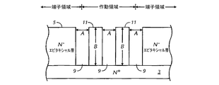
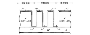
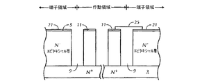
図1から図11は、本発明の第1の好ましい実施例による、従来の端子を備えた超接合装置の製造方法を示す。
20 ゲート(ゲート電極層)
22 イオン打ち込み(イオン打ち込み領域)
24 ゲート酸化物(ゲート酸化物層)
26 ゲート導電体
28 絶縁材料
Claims (22)
- 相互に対向する第1及び第2の主表面を有する半導体基板を設け、この半導体基板は、第2主表面に第1導電率形の強くドープされた領域を有し、第1主表面に第1導電率形の弱くドープされた領域を有し、
上記基板の作動領域に複数個の溝と複数個のメサとを形成し、各溝は、強くドープされた領域に向け、第1主表面から第1深さ位置まで延びる第1延長部分を有し、各メサは側壁面を有し、上記の複数個の溝の各々は、複数個のメサの1つにより、その他の溝の各々から離れていて、
作動領域と、作動領域の外側およびこれに隣接する端子領域内に延びる、複数個のメサと複数個の溝との所定領域上に、誘電体層が、複数個のメサのうち上記所定領域内の各メサの頂部、複数個の溝の各々の両側面および底部ならびに端子領域の頂部を覆うまで上記の誘電体層を形成し、
複数個のメサと複数個の溝との所定領域から上記の誘電体層を取り除いて、複数個の溝の底部にある誘電体層を除去し、
作動領域と端子領域との間の境界の領域上に保護シールドを形成し、
その後複数個のメサと複数個の溝との所定領域の上から保護シールドを部分的に除去し、
複数個のメサと複数個の溝との所定領域の少なくとも1つのメサに、隣接対の溝において、1つの溝の側壁面で、第1導電率形のドーパントを打込み、上記の1つの溝の側壁面に、強くドープされた領域より低いドープ濃度を有する第1導電率形の第1ドープ領域を形成し、
複数個のメサと複数個の溝との所定領域の上記少なくとも1つのメサに、第1導電率形のドーパントを打込んだ側壁に対向する上記の少なくとも1つのメサの側壁面で、第2導電率形のドーパントを打込んで、第1導電率形のドーパントを打込んだ側壁に対向する側壁面に第2導電率形の第2ドープ領域を設ける半導体ディバイスの製造方法によって形成された半導体ディバイス。 - 半導体ディバイスの製造方法であって、
相互に対向する第1及び第2の主表面を有する半導体基板を設け、この半導体基板は、第2主表面に第1導電率形の強くドープされた領域を有し、第1主表面に第1導電率形の弱くドープされた領域を有する、
上記基板の作動領域に複数個の溝と複数個のメサとを形成し、各溝は、強くドープされた領域に向け、第1主表面から第1深さ位置まで延びる第1延長部分を有し、各メサは側壁面を有し、上記の複数個の溝の各々は、複数個のメサの1つにより、その他の溝の各々から離れていて、
作動領域と、作動領域の外側およびこれに隣接する端子領域内に伸びる、複数個のメサと複数個の溝との所定領域に、誘電体層が、複数個のメサのうち上記所定領域内の各メサの頂部、複数個の溝の各々の両側面および底部ならびに端子領域の頂部を覆うまで上記の誘電体層を形成し、
複数個のメサと複数個の溝との所定領域から上記の誘電体層を取除いて、複数個の溝の底部にある誘電体層を除去し、
作動領域と端子領域との間の境界の領域上に保護シールド(遮蔽部)を形成し、
その後複数個のメサと複数個の溝との所定領域の上から保護シールドを部分的に除去し、
複数個のメサと複数個の溝との所定領域の少なくとも1つのメサに、隣接対の溝において、1つの溝の側壁面で、第1導電率形のドーパントをドープし、上記の1つの溝の側壁面に、強くドープされた領域より低いドープ濃度を有する第1導電率形の第1ドープ領域を形成し、
複数個のメサと複数個の溝との所定領域の上記少なくとも1つのメサに、第1導電率形のドーパントを打込んだ側壁に対向する上記の少なくとも1つのメサの側壁面で、第2導電率形のドーパントを、ドープし、第1導電率形のドーパントをドープした側壁に対向する側壁面に第2導電率形の第2ドープ領域を設けるもの。 - 請求項2に記載した半導体ディバイスの製造方法であって、保護シールドを形成する工程が、
複数個のメサと複数個の溝との所定領域の上にフォトレジストの層を沈着させ、
複数個のメサと複数個の溝との所定領域の各側の最後の溝の外側壁上のフォトレジストが保護され、上記の所定領域の残りの個所は保護されないように、マスクを置き、
フォトレジストの保護されていない部分を、紫外線光、深紫外線光、電子ビームおよびX線を含むグループから選ばれたフォトレジスト反応体に晒すことからなるものにおいて、
上記の保護シールドを部分的に除去する工程が
複数個のメサと複数個の溝との所定領域上からマスクを除き、
反応したフォトレジストを構造体から取り除き、
複数個のメサと複数個の溝の所定領域を湿式エッチング法によりエッチングして、反応しなかったフォトレジストにより誘電体層が保護されていた、上記の所定領域の各側の最後の溝の外側壁をのぞいて、上記の所定領域から反応しなかったフォトレジストと誘電体層とを除去し、上記の誘電体層は上記の各最後の溝の外側壁へのイオン打込みを阻止するため残されているもの。 - 請求項3に記載した半導体ディバイスの製造方法であって、
第2ドープ領域と電気的に連結する第3ドープ領域を第1および第2ドープ領域の第1主表面に設け、
第1導電率形の第4ドープ領域を、これが第3ドープ領域を挟んで第1ドープ領域と対向するように、上記の1つの溝の第1主表面と側壁面の少なくとも1方に設け、
ゲート電極層を、第1ドープ領域と第4ドープ領域との間で、ゲート絶縁層を介在させて第3ドープ領域に対向させて設けることからなるもの。 - 請求項4に記載した半導体ディバイスの製造方法であって、ゲート電極層が少なくとも1つの溝に形成されるもの。
- 請求項4に記載した半導体ディバイスの製造方法であって、ゲート電極層が第1主表面上に形成されるもの。
- 請求項2に記載した半導体ディバイスの製造方法であって、保護シールドを形成する工程が、
複数個のメサと複数個の溝との所定領域を乾式エッチング法を用いてエッチングして、複数個の溝の各々の両側部と底部とにある誘電体層を除去し、
マスクを、このマスクの開口部のみが、作動領域の各側の最後の溝とこれに隣接するメサ領域上に位置するように位置決めし、
作動領域の最後の溝とこれに隣接するメサ領域のみが、フォトレジストが沈着する領域であるようにフォトレジストの層をマスク上に沈着させることからなるものにおいて、
部分的に保護シールドを除去する工程が、最後の溝とこれに隣接するメサ領域とを除いて、フォトレジストが沈着するのを阻止したマスクを除去することからなるもの。 - 請求項7に記載した半導体ディバイスの製造方法であって、更に、
第2ドープ領域と電気的に連結する第3ドープ領域を第1および第2ドープ領域の第1主表面に設け、
第1導電率形の第4ドープ領域を、これが第3ドープ領域を挟んで第1ドープ領域と対向するように、上記の複数個の溝の第1主表面と側壁面のいずれかに設け、
ゲート電極層を、第1ドープ領域と第4ドープ領域との間で、ゲート絶縁層を介在させて第3ドープ領域に対向させて設けることからなるもの。 - 請求項7に記載した半導体ディバイスの製造方法であって、ゲート電極層が第1主表面上に形成されるもの。
- 請求項7に記載した半導体ディバイスの製造方法であって、更に、
第2ドープ領域と電気的に連結する第3ドープ領域を第1および第2ドープ領域の第1主表面に設けることからなるもの。 - 請求項7に記載した半導体ディバイスの製造方法であって、更に、電極層を第1ドープ領域とオーム接触させるもの。
- 請求項7に記載した半導体ディバイスの製造方法であって、更に、
半導体ディバイスの製造において第1および第2導電率形のドーパントの各々の拡散長さが、隣接対の溝の側壁面から、第1および第2ドープ領域のP−N接合までの距離より長いもの。 - 請求項2に記載した半導体ディバイスの製造方法であって、更に、
第2ドープ領域と電気的に連結する第3ドープ領域を第1および第2ドープ領域の第1主表面に設けることからなるもの。 - 請求項2に記載した半導体ディバイスの製造方法であって、更に、
電極層を第1ドープ領域とショットキー(Schottky)接触させることからなるもの。 - 請求項2に記載した半導体ディバイスの製造方法であって、
半導体ディバイスの製造において第1および第2導電率形のドーパントの各々の拡散長さが、隣接対の溝の側壁面から、第1および第2ドープ領域のP−N接合までの距離より長いもの。 - 請求項2に記載した半導体ディバイスの製造方法であって、複数個の溝の各側壁面が、第1主表面に対し所定の傾斜角度を維持するもの。
- 請求項2に記載した半導体ディバイスの製造方法であって、乾式エッチング法を用いて、複数個のメサと複数個の溝との所定領域から誘電体層を除去するもの。
- 請求項2に記載した半導体ディバイスの製造方法であって、第1導電率形のドーパントが第1所定打込み角度でドープされるの。
- 請求項2に記載した半導体ディバイスの製造方法であって、第2導電率形のドーパントが第2所定打込み角度でドープされるもの。
- 請求項2に記載した半導体ディバイスの製造方法であって、更に、
複数個の溝に絶縁材料を充填し、
構造体の頂面を平坦化して、
その構造体に超接合装置を形成するもの。 - 請求項2に記載した半導体ディバイスの製造方法によって形成された半導体ディバイス。
- 以下の製造方法によって、形成された半導体ディバイスであって、その方法は、
相互に対向する第1及び第2の主表面を有する半導体基板を設け、上記の半導体基板は、第2主表面に第1導電率形の強くドープされた領域を有し、第1主表面に第1導電率形の弱くドープされた領域を有する、
上記の半導体基板において、その作動領域に複数個の溝と複数個のメサとを形成し、各溝は、強くドープされた領域に向け、第1主表面から第1深さ位置まで延びる第1延長部分を有し、各メサは側壁面を有し、上記の複数個の溝の各々は、複数個のメサの1つにより、その他の溝の各々から離れていて、
作動領域と、作動領域の外側およびこれに隣接する端子領域内に伸びる、複数個のメサと複数個の溝との所定領域を、複数個のメサのうち上記所定領域内の各メサの頂部、複数個の溝の各々の両側面および底部ならびに端子領域の頂部を酸化物が覆うまで酸化し、
複数個のメサと複数個の溝との所定領域とをエッチングして、複数個の溝の底部にある酸化物を除去し、
作動領域と端子領域との間の境界の所定領域上に保護シールドを形成し、
その後複数個のメサと複数個の溝との所定領域の上から保護シールドを部分的に除去し、
複数個のメサと複数個の溝との所定領域の上記少なくとも1つのメサに、隣接対の溝において、1つの溝の側壁面で、第1導電率形のドーパントを打込み、上記の1つの溝の側壁面に、強くドープされた領域より低いドープ濃度を有する第1導電率形の第1ドープ領域を形成し、
複数個のメサと複数個の溝との所定領域の少なくとも1つのメサに、第1導電率形のドーパントを打込んだ側壁に対向する上記の少なくとも1つのメサの側壁面で、第2導電率形のドーパントを打込んで、第1導電率形のドーパントを打込んだ側壁に対向する側壁面に第2導電率形の第2ドープ領域を設け、
複数個の溝に絶縁材料を充填し、
構造体の頂面を平坦化することからなるもの。
Applications Claiming Priority (2)
| Application Number | Priority Date | Filing Date | Title |
|---|---|---|---|
| US53150103P | 2003-12-19 | 2003-12-19 | |
| US60/531,501 | 2003-12-19 |
Related Parent Applications (1)
| Application Number | Title | Priority Date | Filing Date |
|---|---|---|---|
| JP2006545755A Division JP2007515079A (ja) | 2003-12-19 | 2004-12-10 | 従来の端子を備えた超接合装置の製造方法 |
Publications (2)
| Publication Number | Publication Date |
|---|---|
| JP2009004805A true JP2009004805A (ja) | 2009-01-08 |
| JP5154347B2 JP5154347B2 (ja) | 2013-02-27 |
Family
ID=34748768
Family Applications (2)
| Application Number | Title | Priority Date | Filing Date |
|---|---|---|---|
| JP2006545755A Pending JP2007515079A (ja) | 2003-12-19 | 2004-12-10 | 従来の端子を備えた超接合装置の製造方法 |
| JP2008227992A Expired - Fee Related JP5154347B2 (ja) | 2003-12-19 | 2008-09-05 | 超接合半導体ディバイスおよび超接合半導体ディバイスの製造方法 |
Family Applications Before (1)
| Application Number | Title | Priority Date | Filing Date |
|---|---|---|---|
| JP2006545755A Pending JP2007515079A (ja) | 2003-12-19 | 2004-12-10 | 従来の端子を備えた超接合装置の製造方法 |
Country Status (6)
| Country | Link |
|---|---|
| US (2) | US7041560B2 (ja) |
| EP (1) | EP1701686A4 (ja) |
| JP (2) | JP2007515079A (ja) |
| KR (2) | KR20080100265A (ja) |
| TW (1) | TWI368948B (ja) |
| WO (1) | WO2005065140A2 (ja) |
Cited By (1)
| Publication number | Priority date | Publication date | Assignee | Title |
|---|---|---|---|---|
| US12477786B2 (en) | 2022-03-04 | 2025-11-18 | Kabushiki Kaisha Toshiba | Semiconductor device |
Families Citing this family (47)
| Publication number | Priority date | Publication date | Assignee | Title |
|---|---|---|---|---|
| US7638841B2 (en) | 2003-05-20 | 2009-12-29 | Fairchild Semiconductor Corporation | Power semiconductor devices and methods of manufacture |
| KR100994719B1 (ko) * | 2003-11-28 | 2010-11-16 | 페어차일드코리아반도체 주식회사 | 슈퍼정션 반도체장치 |
| KR20080100265A (ko) * | 2003-12-19 | 2008-11-14 | 써드 디멘존 세미컨덕터, 인코포레이티드 | 종래의 종단을 갖는 수퍼 접합 장치를 제조하는 방법 |
| EP1706899A4 (en) * | 2003-12-19 | 2008-11-26 | Third Dimension 3D Sc Inc | PLANARIZATION PROCESS FOR PRODUCING A SUPERJUNCTION COMPONENT |
| US6982193B2 (en) * | 2004-05-10 | 2006-01-03 | Semiconductor Components Industries, L.L.C. | Method of forming a super-junction semiconductor device |
| TWI401749B (zh) | 2004-12-27 | 2013-07-11 | 3D半導體股份有限公司 | 用於高電壓超接面終止之方法 |
| US7439583B2 (en) | 2004-12-27 | 2008-10-21 | Third Dimension (3D) Semiconductor, Inc. | Tungsten plug drain extension |
| EP1872396A4 (en) * | 2005-04-22 | 2009-09-23 | Icemos Technology Corp | SUPERIOR CONSTRUCTION ELEMENT WITH OXIDICALLY DRIED GRATES AND METHOD FOR PRODUCING A SUPER TRANSITION ELEMENT WITH OXIDIDE-DRESSED GRATES |
| US7446018B2 (en) | 2005-08-22 | 2008-11-04 | Icemos Technology Corporation | Bonded-wafer superjunction semiconductor device |
| US7429772B2 (en) | 2006-04-27 | 2008-09-30 | Icemos Technology Corporation | Technique for stable processing of thin/fragile substrates |
| US7948033B2 (en) | 2007-02-06 | 2011-05-24 | Semiconductor Components Industries, Llc | Semiconductor device having trench edge termination structure |
| US7723172B2 (en) | 2007-04-23 | 2010-05-25 | Icemos Technology Ltd. | Methods for manufacturing a trench type semiconductor device having a thermally sensitive refill material |
| US8580651B2 (en) * | 2007-04-23 | 2013-11-12 | Icemos Technology Ltd. | Methods for manufacturing a trench type semiconductor device having a thermally sensitive refill material |
| CN101868856B (zh) | 2007-09-21 | 2014-03-12 | 飞兆半导体公司 | 用于功率器件的超结结构及制造方法 |
| US20090085148A1 (en) * | 2007-09-28 | 2009-04-02 | Icemos Technology Corporation | Multi-directional trenching of a plurality of dies in manufacturing superjunction devices |
| US9484451B2 (en) | 2007-10-05 | 2016-11-01 | Vishay-Siliconix | MOSFET active area and edge termination area charge balance |
| ITMI20072341A1 (it) * | 2007-12-14 | 2009-06-15 | St Microelectronics Srl | Contatti profondi di dispositivi elettronici integrati basati su regioni inpiantate attraverso solchi |
| CN101510557B (zh) | 2008-01-11 | 2013-08-14 | 艾斯莫斯技术有限公司 | 具有电介质终止的超结半导体器件及制造该器件的方法 |
| US7846821B2 (en) | 2008-02-13 | 2010-12-07 | Icemos Technology Ltd. | Multi-angle rotation for ion implantation of trenches in superjunction devices |
| US7795045B2 (en) * | 2008-02-13 | 2010-09-14 | Icemos Technology Ltd. | Trench depth monitor for semiconductor manufacturing |
| US8030133B2 (en) * | 2008-03-28 | 2011-10-04 | Icemos Technology Ltd. | Method of fabricating a bonded wafer substrate for use in MEMS structures |
| US7807576B2 (en) * | 2008-06-20 | 2010-10-05 | Fairchild Semiconductor Corporation | Structure and method for forming a thick bottom dielectric (TBD) for trench-gate devices |
| US20120273916A1 (en) | 2011-04-27 | 2012-11-01 | Yedinak Joseph A | Superjunction Structures for Power Devices and Methods of Manufacture |
| US20110198689A1 (en) * | 2010-02-17 | 2011-08-18 | Suku Kim | Semiconductor devices containing trench mosfets with superjunctions |
| US8598654B2 (en) | 2011-03-16 | 2013-12-03 | Fairchild Semiconductor Corporation | MOSFET device with thick trench bottom oxide |
| US8673700B2 (en) | 2011-04-27 | 2014-03-18 | Fairchild Semiconductor Corporation | Superjunction structures for power devices and methods of manufacture |
| US8786010B2 (en) | 2011-04-27 | 2014-07-22 | Fairchild Semiconductor Corporation | Superjunction structures for power devices and methods of manufacture |
| US8772868B2 (en) | 2011-04-27 | 2014-07-08 | Fairchild Semiconductor Corporation | Superjunction structures for power devices and methods of manufacture |
| US8836028B2 (en) | 2011-04-27 | 2014-09-16 | Fairchild Semiconductor Corporation | Superjunction structures for power devices and methods of manufacture |
| CN103094067B (zh) * | 2011-10-31 | 2015-10-14 | 上海华虹宏力半导体制造有限公司 | 一种半导体器件的制造方法 |
| US9431249B2 (en) | 2011-12-01 | 2016-08-30 | Vishay-Siliconix | Edge termination for super junction MOSFET devices |
| US9614043B2 (en) | 2012-02-09 | 2017-04-04 | Vishay-Siliconix | MOSFET termination trench |
| TWI446459B (zh) * | 2012-02-14 | 2014-07-21 | 茂達電子股份有限公司 | 具有超級介面之功率電晶體元件之製作方法 |
| US8946814B2 (en) | 2012-04-05 | 2015-02-03 | Icemos Technology Ltd. | Superjunction devices having narrow surface layout of terminal structures, buried contact regions and trench gates |
| US9842911B2 (en) | 2012-05-30 | 2017-12-12 | Vishay-Siliconix | Adaptive charge balanced edge termination |
| US9576842B2 (en) | 2012-12-10 | 2017-02-21 | Icemos Technology, Ltd. | Grass removal in patterned cavity etching |
| US9508596B2 (en) | 2014-06-20 | 2016-11-29 | Vishay-Siliconix | Processes used in fabricating a metal-insulator-semiconductor field effect transistor |
| US9887259B2 (en) | 2014-06-23 | 2018-02-06 | Vishay-Siliconix | Modulated super junction power MOSFET devices |
| CN106575666B (zh) | 2014-08-19 | 2021-08-06 | 维西埃-硅化物公司 | 超结金属氧化物半导体场效应晶体管 |
| CN104465402B (zh) * | 2014-12-25 | 2018-03-06 | 中航(重庆)微电子有限公司 | 一种半导体器件制备工艺 |
| CN110993557A (zh) * | 2018-10-02 | 2020-04-10 | 英飞凌科技奥地利有限公司 | 用于在半导体主体中形成绝缘层的方法和晶体管器件 |
| DE102018130444B4 (de) * | 2018-11-30 | 2025-01-23 | Infineon Technologies Austria Ag | Verfahren zum Herstellen eines Superjunction-Transistorbauelements |
| CN111628034B (zh) * | 2020-05-28 | 2023-09-15 | 湖北京邦科技有限公司 | 光电探测装置的制造方法 |
| CN112289684B (zh) * | 2020-10-28 | 2023-06-30 | 上海华虹宏力半导体制造有限公司 | 功率器件的制作方法及器件 |
| US11769665B2 (en) * | 2022-01-11 | 2023-09-26 | Applied Materials, Inc. | Power device structures and methods of making |
| DE102023209573A1 (de) * | 2023-09-29 | 2025-04-03 | Robert Bosch Gesellschaft mit beschränkter Haftung | Verfahren zum Herstellen eines Leistungshalbleiterbauelements mit einer Vielzahl von Finnen und daraus hergestelltes Leistungshalbleiterbauelement |
| CN119584606A (zh) * | 2025-02-07 | 2025-03-07 | 深圳天狼芯半导体有限公司 | 超结垂直双扩散金属氧化物半导体器件及其制备方法 |
Citations (10)
| Publication number | Priority date | Publication date | Assignee | Title |
|---|---|---|---|---|
| JPH0653315A (ja) * | 1992-07-30 | 1994-02-25 | Nec Corp | 半導体装置およびその製造方法 |
| JPH10223896A (ja) * | 1997-02-10 | 1998-08-21 | Mitsubishi Electric Corp | 高耐圧半導体装置およびその製造方法 |
| JP2001015752A (ja) * | 1998-11-11 | 2001-01-19 | Fuji Electric Co Ltd | 超接合半導体素子およびその製造方法 |
| JP2001230413A (ja) * | 2000-02-17 | 2001-08-24 | Fuji Electric Co Ltd | 半導体素子 |
| JP2002015752A (ja) * | 2000-06-30 | 2002-01-18 | Aisin Takaoka Ltd | 燃料電池セパレータの製造方法および製造装置 |
| JP2002124675A (ja) * | 2000-10-16 | 2002-04-26 | Toshiba Corp | 半導体装置およびその製造方法 |
| JP2002170955A (ja) * | 2000-09-25 | 2002-06-14 | Toshiba Corp | 半導体装置およびその製造方法 |
| JP2002230413A (ja) * | 2001-02-06 | 2002-08-16 | Makoto Yamada | 広告配信システム及びその方法 |
| WO2003065459A1 (en) * | 2002-01-28 | 2003-08-07 | Mitsubishi Denki Kabushiki Kaisha | Semiconductor device |
| JP4090518B2 (ja) * | 1998-07-23 | 2008-05-28 | 三菱電機株式会社 | 半導体装置およびその製造方法 |
Family Cites Families (49)
| Publication number | Priority date | Publication date | Assignee | Title |
|---|---|---|---|---|
| US4158206A (en) | 1977-02-07 | 1979-06-12 | Rca Corporation | Semiconductor device |
| JPS5553462A (en) | 1978-10-13 | 1980-04-18 | Int Rectifier Corp | Mosfet element |
| US5057444A (en) * | 1985-03-05 | 1991-10-15 | Matsushita Electric Industrial Co., Ltd. | Method of fabricating semiconductor device |
| US5045903A (en) | 1988-05-17 | 1991-09-03 | Advanced Power Technology, Inc. | Topographic pattern delineated power MOSFET with profile tailored recessed source |
| US4895810A (en) | 1986-03-21 | 1990-01-23 | Advanced Power Technology, Inc. | Iopographic pattern delineated power mosfet with profile tailored recessed source |
| US5019522A (en) | 1986-03-21 | 1991-05-28 | Advanced Power Technology, Inc. | Method of making topographic pattern delineated power MOSFET with profile tailored recessed source |
| US5472888A (en) | 1988-02-25 | 1995-12-05 | International Rectifier Corporation | Depletion mode power MOSFET with refractory gate and method of making same |
| CN1019720B (zh) | 1991-03-19 | 1992-12-30 | 电子科技大学 | 半导体功率器件 |
| EP0512607B1 (en) * | 1991-05-03 | 1997-07-16 | Koninklijke Philips Electronics N.V. | Method of manufacturing a semiconductor device using ion implantation |
| US5366914A (en) | 1992-01-29 | 1994-11-22 | Nec Corporation | Vertical power MOSFET structure having reduced cell area |
| US5506421A (en) | 1992-11-24 | 1996-04-09 | Cree Research, Inc. | Power MOSFET in silicon carbide |
| CN1035294C (zh) | 1993-10-29 | 1997-06-25 | 电子科技大学 | 具有异形掺杂岛的半导体器件耐压层 |
| US5435888A (en) | 1993-12-06 | 1995-07-25 | Sgs-Thomson Microelectronics, Inc. | Enhanced planarization technique for an integrated circuit |
| DE4404757C2 (de) * | 1994-02-15 | 1998-08-20 | Siemens Ag | Verfahren zur Herstellung eines einem Graben benachbarten Diffusionsgebietes in einem Substrat |
| WO1997029518A1 (de) | 1996-02-05 | 1997-08-14 | Siemens Aktiengesellschaft | Durch feldeffekt steuerbares halbleiterbauelement |
| US5744994A (en) | 1996-05-15 | 1998-04-28 | Siliconix Incorporated | Three-terminal power mosfet switch for use as synchronous rectifier or voltage clamp |
| KR0183886B1 (ko) | 1996-06-17 | 1999-04-15 | 김광호 | 반도체장치의 트렌치 소자분리 방법 |
| JP3327135B2 (ja) | 1996-09-09 | 2002-09-24 | 日産自動車株式会社 | 電界効果トランジスタ |
| JP3607016B2 (ja) | 1996-10-02 | 2005-01-05 | 株式会社半導体エネルギー研究所 | 半導体装置およびその作製方法、並びに携帯型の情報処理端末、ヘッドマウントディスプレイ、ナビゲーションシステム、携帯電話、カメラおよびプロジェクター |
| CN1199926A (zh) * | 1997-05-21 | 1998-11-25 | 日本电气株式会社 | 一种半导体器件的制造方法 |
| JP3618517B2 (ja) | 1997-06-18 | 2005-02-09 | 三菱電機株式会社 | 半導体装置およびその製造方法 |
| US5976947A (en) | 1997-08-18 | 1999-11-02 | Micron Technology, Inc. | Method for forming dielectric within a recess |
| US6239463B1 (en) | 1997-08-28 | 2001-05-29 | Siliconix Incorporated | Low resistance power MOSFET or other device containing silicon-germanium layer |
| US6081009A (en) * | 1997-11-10 | 2000-06-27 | Intersil Corporation | High voltage mosfet structure |
| DE19801095B4 (de) | 1998-01-14 | 2007-12-13 | Infineon Technologies Ag | Leistungs-MOSFET |
| US6265282B1 (en) * | 1998-08-17 | 2001-07-24 | Micron Technology, Inc. | Process for making an isolation structure |
| US6355580B1 (en) * | 1998-09-03 | 2002-03-12 | Micron Technology, Inc. | Ion-assisted oxidation methods and the resulting structures |
| US6291856B1 (en) | 1998-11-12 | 2001-09-18 | Fuji Electric Co., Ltd. | Semiconductor device with alternating conductivity type layer and method of manufacturing the same |
| DE19854915C2 (de) | 1998-11-27 | 2002-09-05 | Infineon Technologies Ag | MOS-Feldeffekttransistor mit Hilfselektrode |
| DE69833743T2 (de) | 1998-12-09 | 2006-11-09 | Stmicroelectronics S.R.L., Agrate Brianza | Herstellungmethode einer integrierte Randstruktur für Hochspannung-Halbleiteranordnungen |
| US6452230B1 (en) | 1998-12-23 | 2002-09-17 | International Rectifier Corporation | High voltage mosgated device with trenches to reduce on-resistance |
| US6190970B1 (en) | 1999-01-04 | 2001-02-20 | Industrial Technology Research Institute | Method of making power MOSFET and IGBT with optimized on-resistance and breakdown voltage |
| US6346442B1 (en) * | 1999-02-04 | 2002-02-12 | Tower Semiconductor Ltd. | Methods for fabricating a semiconductor chip having CMOS devices and a fieldless array |
| US6222229B1 (en) | 1999-02-18 | 2001-04-24 | Cree, Inc. | Self-aligned shield structure for realizing high frequency power MOSFET devices with improved reliability |
| US6198127B1 (en) | 1999-05-19 | 2001-03-06 | Intersil Corporation | MOS-gated power device having extended trench and doping zone and process for forming same |
| EP1058303A1 (en) | 1999-05-31 | 2000-12-06 | STMicroelectronics S.r.l. | Fabrication of VDMOS structure with reduced parasitic effects |
| DE19964214C2 (de) | 1999-09-07 | 2002-01-17 | Infineon Technologies Ag | Verfahren zur Herstellung einer Driftzone eines Kompensationsbauelements |
| GB9929613D0 (en) | 1999-12-15 | 2000-02-09 | Koninkl Philips Electronics Nv | Manufacture of semiconductor material and devices using that material |
| US6214698B1 (en) | 2000-01-11 | 2001-04-10 | Taiwan Semiconductor Manufacturing Company | Shallow trench isolation methods employing gap filling doped silicon oxide dielectric layer |
| JP4088033B2 (ja) * | 2000-11-27 | 2008-05-21 | 株式会社東芝 | 半導体装置 |
| US6509220B2 (en) | 2000-11-27 | 2003-01-21 | Power Integrations, Inc. | Method of fabricating a high-voltage transistor |
| US6608350B2 (en) | 2000-12-07 | 2003-08-19 | International Rectifier Corporation | High voltage vertical conduction superjunction semiconductor device |
| US6424007B1 (en) | 2001-01-24 | 2002-07-23 | Power Integrations, Inc. | High-voltage transistor with buried conduction layer |
| US6465325B2 (en) | 2001-02-27 | 2002-10-15 | Fairchild Semiconductor Corporation | Process for depositing and planarizing BPSG for dense trench MOSFET application |
| EP1267415A3 (en) * | 2001-06-11 | 2009-04-15 | Kabushiki Kaisha Toshiba | Power semiconductor device having resurf layer |
| EP1706900A4 (en) * | 2003-12-19 | 2009-07-22 | Third Dimension 3D Sc Inc | METHOD FOR PRODUCING A SUPERJUNCTION COMPONENT WITH WIDE MESAS |
| EP1706899A4 (en) * | 2003-12-19 | 2008-11-26 | Third Dimension 3D Sc Inc | PLANARIZATION PROCESS FOR PRODUCING A SUPERJUNCTION COMPONENT |
| KR20080100265A (ko) * | 2003-12-19 | 2008-11-14 | 써드 디멘존 세미컨덕터, 인코포레이티드 | 종래의 종단을 갖는 수퍼 접합 장치를 제조하는 방법 |
| US7023069B2 (en) * | 2003-12-19 | 2006-04-04 | Third Dimension (3D) Semiconductor, Inc. | Method for forming thick dielectric regions using etched trenches |
-
2004
- 2004-12-10 KR KR1020087022910A patent/KR20080100265A/ko not_active Withdrawn
- 2004-12-10 KR KR1020067014535A patent/KR20070032624A/ko not_active Ceased
- 2004-12-10 JP JP2006545755A patent/JP2007515079A/ja active Pending
- 2004-12-10 EP EP04813607A patent/EP1701686A4/en not_active Withdrawn
- 2004-12-10 US US11/009,678 patent/US7041560B2/en not_active Expired - Fee Related
- 2004-12-10 WO PCT/US2004/041302 patent/WO2005065140A2/en not_active Ceased
- 2004-12-17 TW TW093139450A patent/TWI368948B/zh not_active IP Right Cessation
-
2006
- 2006-03-21 US US11/385,155 patent/US7704864B2/en not_active Expired - Fee Related
-
2008
- 2008-09-05 JP JP2008227992A patent/JP5154347B2/ja not_active Expired - Fee Related
Patent Citations (10)
| Publication number | Priority date | Publication date | Assignee | Title |
|---|---|---|---|---|
| JPH0653315A (ja) * | 1992-07-30 | 1994-02-25 | Nec Corp | 半導体装置およびその製造方法 |
| JPH10223896A (ja) * | 1997-02-10 | 1998-08-21 | Mitsubishi Electric Corp | 高耐圧半導体装置およびその製造方法 |
| JP4090518B2 (ja) * | 1998-07-23 | 2008-05-28 | 三菱電機株式会社 | 半導体装置およびその製造方法 |
| JP2001015752A (ja) * | 1998-11-11 | 2001-01-19 | Fuji Electric Co Ltd | 超接合半導体素子およびその製造方法 |
| JP2001230413A (ja) * | 2000-02-17 | 2001-08-24 | Fuji Electric Co Ltd | 半導体素子 |
| JP2002015752A (ja) * | 2000-06-30 | 2002-01-18 | Aisin Takaoka Ltd | 燃料電池セパレータの製造方法および製造装置 |
| JP2002170955A (ja) * | 2000-09-25 | 2002-06-14 | Toshiba Corp | 半導体装置およびその製造方法 |
| JP2002124675A (ja) * | 2000-10-16 | 2002-04-26 | Toshiba Corp | 半導体装置およびその製造方法 |
| JP2002230413A (ja) * | 2001-02-06 | 2002-08-16 | Makoto Yamada | 広告配信システム及びその方法 |
| WO2003065459A1 (en) * | 2002-01-28 | 2003-08-07 | Mitsubishi Denki Kabushiki Kaisha | Semiconductor device |
Cited By (1)
| Publication number | Priority date | Publication date | Assignee | Title |
|---|---|---|---|---|
| US12477786B2 (en) | 2022-03-04 | 2025-11-18 | Kabushiki Kaisha Toshiba | Semiconductor device |
Also Published As
| Publication number | Publication date |
|---|---|
| TW200531280A (en) | 2005-09-16 |
| KR20080100265A (ko) | 2008-11-14 |
| EP1701686A4 (en) | 2009-07-01 |
| US20050181558A1 (en) | 2005-08-18 |
| US7041560B2 (en) | 2006-05-09 |
| JP5154347B2 (ja) | 2013-02-27 |
| EP1701686A2 (en) | 2006-09-20 |
| WO2005065140A2 (en) | 2005-07-21 |
| WO2005065140A3 (en) | 2006-10-12 |
| US7704864B2 (en) | 2010-04-27 |
| KR20070032624A (ko) | 2007-03-22 |
| JP2007515079A (ja) | 2007-06-07 |
| US20060160309A1 (en) | 2006-07-20 |
| TWI368948B (en) | 2012-07-21 |
Similar Documents
| Publication | Publication Date | Title |
|---|---|---|
| JP5154347B2 (ja) | 超接合半導体ディバイスおよび超接合半導体ディバイスの製造方法 | |
| JP4928947B2 (ja) | 超接合デバイスの製造方法 | |
| US9385202B2 (en) | Semiconductor device having a patterned gate dielectric | |
| JP5379045B2 (ja) | トレンチ金属酸化膜半導体素子 | |
| JP5309058B2 (ja) | トレンチ金属酸化膜半導体素子及び終端構造の製造方法 | |
| US8889532B2 (en) | Method of making an insulated gate semiconductor device and structure | |
| TWI591789B (zh) | 用於製造具有一屏蔽電極結構之一絕緣閘極半導體裝置之方法 | |
| CN111081779B (zh) | 一种屏蔽栅沟槽式mosfet及其制造方法 | |
| US8889513B2 (en) | Trench MOSFET with trenched floating gates having thick trench bottom oxide as termination | |
| CN101764159B (zh) | 带有减小的击穿电压的金属氧化物半导体场效应管器件 | |
| JP4417962B2 (ja) | 超接合デバイスの製造での平坦化方法 | |
| TWI412071B (zh) | 自對準電荷平衡的功率雙擴散金屬氧化物半導體製備方法 | |
| CN210296383U (zh) | Mosfet器件和碳化硅mosfet器件 | |
| CN111180522B (zh) | 具有超结和嵌氧硅层的半导体器件 | |
| CN101114583B (zh) | 半导体功率器件及其制造工艺 | |
| JP4100071B2 (ja) | 半導体装置 | |
| CN118352390A (zh) | 超结半导体器件及其制造方法 |
Legal Events
| Date | Code | Title | Description |
|---|---|---|---|
| A977 | Report on retrieval |
Free format text: JAPANESE INTERMEDIATE CODE: A971007 Effective date: 20110922 |
|
| A131 | Notification of reasons for refusal |
Free format text: JAPANESE INTERMEDIATE CODE: A131 Effective date: 20110929 |
|
| A521 | Request for written amendment filed |
Free format text: JAPANESE INTERMEDIATE CODE: A523 Effective date: 20111227 |
|
| A131 | Notification of reasons for refusal |
Free format text: JAPANESE INTERMEDIATE CODE: A131 Effective date: 20120412 |
|
| A601 | Written request for extension of time |
Free format text: JAPANESE INTERMEDIATE CODE: A601 Effective date: 20120712 |
|
| A602 | Written permission of extension of time |
Free format text: JAPANESE INTERMEDIATE CODE: A602 Effective date: 20120718 |
|
| A601 | Written request for extension of time |
Free format text: JAPANESE INTERMEDIATE CODE: A601 Effective date: 20120810 |
|
| A602 | Written permission of extension of time |
Free format text: JAPANESE INTERMEDIATE CODE: A602 Effective date: 20120815 |
|
| A601 | Written request for extension of time |
Free format text: JAPANESE INTERMEDIATE CODE: A601 Effective date: 20120912 |
|
| A602 | Written permission of extension of time |
Free format text: JAPANESE INTERMEDIATE CODE: A602 Effective date: 20120918 |
|
| A521 | Request for written amendment filed |
Free format text: JAPANESE INTERMEDIATE CODE: A523 Effective date: 20121012 |
|
| TRDD | Decision of grant or rejection written | ||
| A01 | Written decision to grant a patent or to grant a registration (utility model) |
Free format text: JAPANESE INTERMEDIATE CODE: A01 Effective date: 20121108 |
|
| A61 | First payment of annual fees (during grant procedure) |
Free format text: JAPANESE INTERMEDIATE CODE: A61 Effective date: 20121205 |
|
| FPAY | Renewal fee payment (event date is renewal date of database) |
Free format text: PAYMENT UNTIL: 20151214 Year of fee payment: 3 |
|
| R150 | Certificate of patent or registration of utility model |
Free format text: JAPANESE INTERMEDIATE CODE: R150 |
|
| LAPS | Cancellation because of no payment of annual fees |