JP2009013003A - Diamond manufacturing method and manufacturing apparatus - Google Patents
Diamond manufacturing method and manufacturing apparatus Download PDFInfo
- Publication number
- JP2009013003A JP2009013003A JP2007175772A JP2007175772A JP2009013003A JP 2009013003 A JP2009013003 A JP 2009013003A JP 2007175772 A JP2007175772 A JP 2007175772A JP 2007175772 A JP2007175772 A JP 2007175772A JP 2009013003 A JP2009013003 A JP 2009013003A
- Authority
- JP
- Japan
- Prior art keywords
- diamond
- holder
- substrate
- deposited
- film
- Prior art date
- Legal status (The legal status is an assumption and is not a legal conclusion. Google has not performed a legal analysis and makes no representation as to the accuracy of the status listed.)
- Pending
Links
Images


Landscapes
- Crystals, And After-Treatments Of Crystals (AREA)
- Carbon And Carbon Compounds (AREA)
- Chemical Vapour Deposition (AREA)
Abstract
【課題】ダイヤモンド生成工程の際の放熱ホルダ上におけるダイヤモンド膜の剥離等による不良発生や、異常成長等を防ぐことを目的とする。
【解決手段】表面にダイヤモンドが蒸着しないホルダを準備し、もしくはダイヤモンドが蒸着した場合でも前記ホルダ温度1300℃〜室温では蒸着したダイヤモンドが剥離せず、またダイヤモンド及び\炭化物が異常成長しないホルダを準備した後、ダイヤモンドを成膜する基板を該ホルダ上に設置した後、該基板上にダイヤモンドの成膜を行うことを特徴とするダイヤモンド製造方法及び製造装置である。前記ホルダの基板近傍が表面粗さRa0.01μm以下であることが好ましい。
【選択図】図1An object of the present invention is to prevent occurrence of defects due to peeling of a diamond film on a heat dissipation holder during a diamond generation process, abnormal growth, and the like.
A holder is prepared in which diamond is not deposited on the surface, or even when diamond is deposited, a holder in which the deposited diamond does not peel at the holder temperature of 1300 ° C. to room temperature and diamond and carbide do not grow abnormally is prepared. Then, a diamond manufacturing method and a manufacturing apparatus are characterized in that after a substrate on which a diamond film is formed is placed on the holder, a diamond film is formed on the substrate. It is preferable that the vicinity of the substrate of the holder has a surface roughness Ra of 0.01 μm or less.
[Selection] Figure 1
Description
本発明は、ダイヤモンド製造方法及び製造装置に関し、ダイヤモンドを成膜する基板を設置するための放熱ホルダ上に蒸着したダイヤモンド、炭化物が剥離して飛散することによる成膜不良等を防ぐダイヤモンド製造方法及び製造装置に関するものである。 The present invention relates to a diamond manufacturing method and a manufacturing apparatus, and relates to a diamond manufacturing method and a diamond manufacturing method for preventing deposition failure caused by separation and scattering of diamond deposited on a heat dissipating holder for setting a substrate on which diamond is deposited, and carbide. The present invention relates to a manufacturing apparatus.
ダイヤモンドは高熱伝導率、高い電子・正孔移動度、高い絶縁破壊電界強度、低誘電損失、そして広いバンドギャップといった、半導体材料として他に類を見ない優れた特性を数多く備えている。特に近年では、広いバンドギャップを活かした紫外発光素子や、優れた高周波特性を持つ電界効果トランジスタなどが開発されつつある。
ダイヤモンドを製造するにあたって様々な方法が試みられているが、加熱フィラメントを用いる方法、マイクロ波等により励起したプラズマを用いる方法がある。その他特殊なものとして、火炎法、スパッタリング法、イオンビーム法、紫外線放射などがあり、これらの励起手段により、メタン等炭化水素と水素の混合ガスを分解励起し、基板などの上にダイヤモンドを析出させることができる。
Diamond has many unique properties that are unparalleled as a semiconductor material, such as high thermal conductivity, high electron / hole mobility, high breakdown field strength, low dielectric loss, and wide band gap. In particular, in recent years, ultraviolet light emitting elements utilizing a wide band gap and field effect transistors having excellent high frequency characteristics are being developed.
Various methods have been tried to produce diamond, and there are a method using a heating filament and a method using plasma excited by a microwave or the like. Other special ones include flame method, sputtering method, ion beam method, ultraviolet radiation, etc. With these excitation means, a mixed gas of hydrocarbon and hydrogen such as methane is decomposed and excited, and diamond is deposited on the substrate etc. Can be made.
例えばマイクロ波プラズマCVDで成膜する場合には、メタンガスなどの炭素系ガスと水素ガスを混合したガスを用い、減圧及び800〜1200℃程度に上昇させることで基板上へダイヤモンド生成が可能である。この方法を行なう場合には、ダイヤモンドを生成させる基板から放熱させる必要がある。一般的には前記基板を放熱ホルダ上に設置した後に基板上へのダイヤモンドの生成を行う。
この際、ダイヤモンドが成膜する基板面の反対側の面、もしくは基板の側面を放熱ホルダと接触させて設置する。更にその放熱ホルダと熱エネルギーを受け取るためのステージとを接触させ、このステージを水冷などさせることで放熱を行う。前記基板を設置するための前記放熱ホルダは、モリブデンなどの高い融点及び高い熱伝導率をもつ材料が一般的に使用されている(特許文献1参照)。
At this time, the surface opposite to the substrate surface on which diamond is deposited, or the side surface of the substrate is placed in contact with the heat dissipation holder. Further, the heat radiation holder is brought into contact with a stage for receiving thermal energy, and heat is radiated by cooling the stage with water. A material having a high melting point and high thermal conductivity such as molybdenum is generally used for the heat dissipation holder for installing the substrate (see Patent Document 1).
基板上にダイヤモンドの成膜を行う際に、同時にモリブデンなどの材料を用いた放熱ホルダ上にもダイヤモンドや炭化物が蒸着し、この蒸着したダイヤモンドや炭化物が、合成中等に剥離を起こすことがある。そして剥離して飛散したダイヤモンドや炭化物が、本来ダイヤモンドの成膜を行なうべき基板に付着することで、成膜不良が生じる等の問題が発生する。また、異常成長と呼ばれる、ダイヤモンドもしくは炭化物が生成されたものが急激に増大した場合に起こる合成不良といった問題が発生する。本発明はダイヤモンド生成工程における不良発生や異常成長等を防止することを目的とする。 When a diamond film is formed on the substrate, diamond or carbide may be deposited on a heat dissipation holder using a material such as molybdenum, and the deposited diamond or carbide may be peeled off during synthesis. Then, the diamond or carbide that has been peeled off and scattered adheres to the substrate on which diamond should be originally formed, thereby causing problems such as film formation defects. In addition, there is a problem called “abnormal growth” such as poor synthesis that occurs when diamonds or carbides generated abruptly increase. An object of the present invention is to prevent occurrence of defects, abnormal growth, and the like in a diamond production process.
本発明は上記課題を解決するために、基板を放熱ホルダに設置してダイヤモンドを成膜する場合において、表面にダイヤモンドが蒸着しない、もしくはダイヤモンドが蒸着した場合でも剥離しない放熱ホルダを用いる点に特徴を有する。すなわちホルダ材質を珪素、炭化珪素などダイヤモンドが剥離しにくい材質を用いる、もしくは表面粗さを小さくするなどの方法を用いることで、ダイヤモンドの蒸着、剥離を防ぐことができ、本来ダイヤモンドを成膜するべき基板の成膜不良を抑制することができる。また、放熱ホルダを分割可能とすることで、ダイヤモンドが厚く成膜されたものでも随時変更が可能となり、剥離し飛散することにより成膜不良を抑制することができる。 In order to solve the above-mentioned problems, the present invention is characterized in that when a substrate is placed on a heat dissipation holder to form a diamond film, a heat dissipation holder that does not deposit diamond on the surface or does not peel even when diamond is deposited is used. Have That is, by using a material such as silicon or silicon carbide that is difficult to peel diamond, or by reducing the surface roughness, the holder material can be prevented from being deposited and peeled off. It is possible to suppress film formation defects on the power substrate. In addition, by making the heat dissipation holder separable, even a thick diamond film can be changed at any time, and film formation defects can be suppressed by peeling and scattering.
本発明は上記課題を解決するために以下の構成を採用する。
(1)気相合成法によってダイヤモンドを生成するダイヤモンド製造方法において、表面にダイヤモンドが蒸着しないホルダを準備し、もしくはダイヤモンドが蒸着した場合でも前記ホルダ温度1300℃〜室温では蒸着したダイヤモンドが剥離せず、またダイヤモンド及び\炭化物が異常成長しないホルダを準備した後、ダイヤモンドを成膜する基板を該ホルダ上に設置した後、該基板上にダイヤモンドの成膜を行うことを特徴とするダイヤモンド製造方法である。
(2)前記ダイヤモンドを成膜する基板を設置するためのホルダの少なくとも基板近傍が、珪素、炭化珪素、窒化珪素、酸化アルミニウム、窒化アルミニウムのいずれかにより形成されていることを特徴とする上記(1)に記載のダイヤモンド製造方法である。
(3)前記ダイヤモンドを成膜する基板を設置するためのホルダの少なくとも基板近傍が、表面粗さRa0.01μm以下であることを特徴とする上記(1)又は(2)に記載のダイヤモンド製造方法である。
(4)前記ダイヤモンドを成膜する基板を設置するためのホルダが分離可能であり、少なくとも一部分が交換可能であることを特徴とする上記(1)〜(3)のいずれかに記載のダイヤモンド製造方法である。
(5)前記ホルダは、基板上にダイヤモンドを成膜する前に予めダイヤモンド、酸化物、窒化物、炭化物のいずれかを成膜しておくことを特徴とする上記(1)〜(4)のいずれかに記載のダイヤモンド製造方法である。
The present invention adopts the following configuration in order to solve the above problems.
(1) In a diamond manufacturing method in which diamond is generated by a vapor phase synthesis method, a holder on which diamond is not deposited is prepared, or even when diamond is deposited, the deposited diamond does not peel at the holder temperature of 1300 ° C. to room temperature. In addition, after preparing a holder on which diamond and carbide do not grow abnormally, a diamond film is formed on the substrate after the substrate on which the diamond film is formed is placed on the holder. is there.
(2) The above (characterized in that at least the vicinity of the holder for setting the substrate on which the diamond film is formed is formed of any one of silicon, silicon carbide, silicon nitride, aluminum oxide, and aluminum nitride. It is a diamond manufacturing method as described in 1).
(3) The method for producing diamond according to (1) or (2) above, wherein at least the vicinity of the substrate for placing the substrate on which the diamond is deposited has a surface roughness Ra of 0.01 μm or less. It is.
(4) The diamond production according to any one of (1) to (3) above, wherein a holder for placing the substrate on which the diamond is to be formed is separable and at least a part of the holder can be replaced. Is the method.
(5) The holder according to any one of (1) to (4) above, wherein any one of diamond, oxide, nitride, and carbide is formed in advance before forming diamond on the substrate. The diamond production method according to any one of the above.
(6)気相合成法によってダイヤモンドを生成するダイヤモンド製造装置において、ダイヤモンドを成膜する基板を設置するためのホルダを有し、当該ホルダが表面にダイヤモンドを蒸着しない、もしくはダイヤモンドが蒸着した場合でも前記ホルダ温度1300℃〜室温では蒸着したダイヤモンドが剥離せず、またダイヤモンド及び\又は炭化物が異常成長しないことを特徴とする製造装置である。
(7)前記ダイヤモンドを成膜する基板を設置するためのホルダの少なくとも基板近傍が、珪素、炭化珪素、窒化珪素、酸化アルミニウム、窒化アルミニウムのいずれかであることを特徴とする上記(6)に記載のダイヤモンド製造装置である。
(8)前記ダイヤモンドを成膜する基板を設置するホルダの少なくとも基板近傍が、表面粗さRa0.01μm以下であることを特徴とする上記(6)又は(7)に記載のダイヤモンド製造装置である。
(9)前記ダイヤモンドを成膜する基板を設置するホルダが分離可能であり、少なくとも一部分が交換可能であることを特徴とする上記(6)〜(8)のいずれかに記載のダイヤモンド製造装置である。
(10)前記ホルダは、基板上にダイヤモンドを成膜する前に予めダイヤモンド、酸化物、窒化物、炭化物のいずれかを成膜しておくことを特徴とする上記(6)〜(9)のいずれかに記載のダイヤモンド製造装置である。
(6) A diamond manufacturing apparatus that generates diamond by a vapor phase synthesis method has a holder for setting a substrate on which a diamond film is to be formed, and the holder does not deposit diamond on the surface or even when diamond is deposited. In the holder temperature of 1300 ° C. to room temperature, the deposited diamond does not peel and diamond and / or carbide do not grow abnormally.
(7) The above (6) is characterized in that at least the substrate vicinity of the holder for setting the substrate on which the diamond is deposited is any one of silicon, silicon carbide, silicon nitride, aluminum oxide, and aluminum nitride. It is a diamond manufacturing apparatus of description.
(8) The diamond manufacturing apparatus according to the above (6) or (7), wherein at least the vicinity of the substrate on which the substrate on which the diamond is to be deposited is placed has a surface roughness Ra of 0.01 μm or less. .
(9) The diamond manufacturing apparatus according to any one of (6) to (8), wherein a holder on which the substrate on which the diamond is to be formed is separable is separable and at least a part of the holder can be replaced. is there.
(10) The holder according to any one of (6) to (9), wherein any one of diamond, oxide, nitride, and carbide is formed in advance before forming the diamond on the substrate. The diamond production apparatus according to any one of the above.
本発明に係るダイヤモンドを成膜する基板の材料としては、単結晶ダイヤモンド、多結晶ダイヤモンド、シリコン基板など種々のものが挙げられる。
また、本発明で用いられるホルダは、特に形状を特定しないが円状、角状などの形状のものが挙げられ、ダイヤモンドを成膜する基板を設置することができる。
さらに異常成長とは、ホルダ上にダイヤモンドもしくは炭化物が生成されたものが、他の部分と比べて速い成膜速度を持ち、ダイヤモンドもしくは炭化物が急激に増大していくことを意味する。マイクロ波プラズマCVD法などを用いる際にこの異常成長が発生すると、異常成長発生部分でプラズマに集中が起こり、周辺での成長条件を変えてしまう。これにより、その他の部分ではダイヤモンドの成膜不良、例えば単結晶の成膜を行っていた場合に、異常成長発生部分にプラズマが集中することで、成長条件が変わり基板上に多結晶が成膜されてしまう。
そこで本発明に係るダイヤモンド製造方法及び製造装置を用いることにより、通常ホルダに蒸着していたダイヤモンドが剥離し飛散することを防ぎ、ダイヤモンドを成膜する目的で設置している基板上へ剥離したダイヤが付着することにより生じていた成膜不良を防ぐことができる。
Examples of the material for the substrate on which the diamond film according to the present invention is formed include various materials such as single crystal diamond, polycrystalline diamond, and silicon substrate.
In addition, the holder used in the present invention is not particularly specified in shape, but may have a circular shape or a rectangular shape, and a substrate on which a diamond film is formed can be placed.
Furthermore, abnormal growth means that diamond or carbide produced on the holder has a higher film formation rate than other parts, and diamond or carbide increases rapidly. If this abnormal growth occurs when using the microwave plasma CVD method or the like, the plasma is concentrated at the abnormal growth occurrence portion, and the growth conditions in the periphery are changed. As a result, in other parts where diamond film formation is poor, for example, when a single crystal film is formed, the plasma concentrates on the part where abnormal growth occurs, so that the growth conditions change and a polycrystalline film is formed on the substrate. Will be.
Therefore, by using the diamond manufacturing method and manufacturing apparatus according to the present invention, the diamond deposited on the holder can be prevented from peeling and scattering, and the diamond peeled onto the substrate installed for the purpose of forming the diamond film. It is possible to prevent film formation defects caused by the adhesion of the film.
次にホルダの材質としては、少なくとも一部が珪素、炭化珪素、窒化珪素、酸化アルミニウム、窒化アルミニウムのいずれかであることが好ましい。例えば、ダイヤモンドを成膜する基板の近傍5mmφ領域を、珪素、炭化珪素、窒化珪素、酸化アルミニウム、窒化アルミニウムで形成することによって、ダイヤモンドがホルダ上に蒸着した場合でも、そのダイヤモンドとの密着力が高く、モリブデン材を使用した時の様に著しく剥離する事はない。よって、基板近傍でダイヤモンドが剥離し、飛散することで基材上にダイヤモンドが付着することによる不良発生を防ぐことができる。
前記ダイヤモンドを成膜する基板を設置するホルダの少なくとも一部の表面粗さがRa0.01μm以下であることが好ましい。表面粗さをRa0.01μm以下にすることにより、前記と同様に基板近傍でダイヤモンドが剥離し、飛散することで基材上にダイヤモンドが付着することによる不良発生を防ぐことができる。
Next, it is preferable that at least a part of the material of the holder is silicon, silicon carbide, silicon nitride, aluminum oxide, or aluminum nitride. For example, by forming a 5 mmφ region in the vicinity of a substrate on which diamond is formed with silicon, silicon carbide, silicon nitride, aluminum oxide, or aluminum nitride, even when diamond is deposited on the holder, the adhesion with the diamond is improved. It is high and does not peel off as much as when using molybdenum material. Therefore, it is possible to prevent the occurrence of defects due to diamond adhering to the base material by peeling and scattering of diamond in the vicinity of the substrate.
It is preferable that the surface roughness of at least a part of the holder on which the substrate on which the diamond film is formed is set is Ra 0.01 μm or less. By setting the surface roughness to Ra 0.01 μm or less, it is possible to prevent the occurrence of defects due to diamond adhering to the base material by peeling and scattering in the vicinity of the substrate in the same manner as described above.
前記ダイヤモンドを成膜する基板を設置するホルダが分離可能であり、少なくとも一部分が交換可能であることが好ましい。これにより、長時間合成することで、万が一ホルダ上にダイヤモンドが蒸着することがあり、更に繰り返し使うことでダイヤモンドの膜厚が大きくなり剥離が起こりやすくなる部分が発生したとしても、剥離する前に予めその部分のみを交換することで剥離を防ぐことができる。例えば、基板を設置している場所の近傍5mm角を交換可能とすることにより、ダイヤモンドが剥離し、飛散することで基材上にダイヤモンドが付着することによる不良発生を抑止することができる。 It is preferable that the holder on which the substrate on which the diamond film is to be formed is separable and at least a part is replaceable. As a result, diamond may be deposited on the holder by synthesizing for a long time, and even if there is a part where the film thickness of diamond is increased and peeling is likely to occur by repeated use, before peeling Separation can be prevented by exchanging only that portion in advance. For example, by making it possible to replace the 5 mm square near the place where the substrate is installed, it is possible to suppress the occurrence of defects due to diamond peeling off and scattering to adhere to the base material.
前記ホルダの交換可能である部分の表面には、ダイヤモンドを成膜する前に予め成膜しておくことが好ましい。長時間の合成を行う場合には、分離可能部分を交換する以前にダイヤモンド膜の剥離や、異常成長が起こってしまう。予め、合成を行っておくことで密着力の良いダイヤモンド膜を形成するか、または酸化物、窒化物、炭化物を成膜しておくことで、ダイヤモンドの剥離を防ぐ、もしくは異常成長を抑制することができる。また分離可能にしておくことで、ダイヤモンド、酸化物、窒化物、炭化物のいずれかを予め表面へ成膜する作業も容易となる。 It is preferable that a film is formed in advance on the surface of the portion where the holder can be replaced before the diamond is formed. When synthesizing for a long time, peeling of the diamond film or abnormal growth occurs before exchanging the separable portion. Forming a diamond film with good adhesion by synthesizing in advance or forming an oxide, nitride, or carbide to prevent diamond peeling or abnormal growth Can do. In addition, by making it separable, it becomes easy to form a film of diamond, oxide, nitride, or carbide on the surface in advance.
本発明ではダイヤモンドを成膜する際に用いるホルダ材質、表面粗さを変更することで、成膜中にダイヤモンド膜が剥離し飛散することによる成膜不良を防ぎ、さらにはダイヤモンドが蒸着しないようにすることで、異常成長が起こることによる成膜条件の変動、成膜不良を防ぐことが可能である。 In the present invention, by changing the holder material and the surface roughness used when depositing diamond, the diamond film is peeled off and scattered during deposition to prevent deposition failure, and further, diamond is not deposited. By doing so, it is possible to prevent film formation condition fluctuations and film formation defects due to abnormal growth.
ホルダ上に基板を設置してダイヤモンドを成膜する場合において、ホルダ表面にダイヤモンドが成膜しない、もしくはダイヤモンドが蒸着した場合でも剥離しないようにする。すなわち、ホルダの材質として珪素、炭化珪素などダイヤモンドが剥離しにくい材質を用いる、表面粗さを小さくするなどの方法を用いる。また、万が一表面にダイヤモンドが成膜される部分ができたとしても、分離し交換可能とする事で、剥離が起こる前にダイヤモンドが成膜された部分を交換することで、剥離、飛散による成膜不良を防ぐことができる。 In the case where a substrate is placed on a holder to form a diamond film, diamond is not formed on the surface of the holder, or is not peeled even when diamond is deposited. That is, the holder is made of a material such as silicon or silicon carbide that is difficult to peel diamond, or the surface roughness is reduced. In addition, even if a diamond film is formed on the surface, it can be separated and replaced. Film defects can be prevented.
本発明のダイヤモンド製造方法及び製造装置により、ダイヤモンド生成工程の際の放熱ホルダ上におけるダイヤモンド膜の剥離等による不良発生や、異常成長等を防ぐことができる。 According to the diamond manufacturing method and manufacturing apparatus of the present invention, it is possible to prevent the occurrence of defects due to peeling of the diamond film on the heat dissipation holder during the diamond production process, abnormal growth, and the like.
以下、本発明を実施例に基づいて詳細に説明する。以下の実施例は本発明の一例であり、本発明を限定するものではない。
[実施例1]
3mm×6mm、厚さ0.7mmの人工Ib型単結晶{100}基板を用意し、基板が設置できる50mmφ−3mmtのホルダを準備した。ホルダ材は、珪素、炭化珪素、窒化珪素、酸化アルミニウム、窒化アルミニウムの5種類で作られたものを、それぞれ準備した。
ホルダに配置された前記基板上へ、マイクロ波プラズマCVDによるエピタキシャル成長を行った。基板温度は1100℃、圧力90torrで実施した。導入したガスはメタン200sccm(standard cubiccm)、水素1000sccmとした。計20時間成膜を行った。
20時間の成膜後、マイクロ波の導入を停止し、室温まで冷却を行なった。
この時に使用した5種類共にホルダ表面にはダイヤモンドの蒸着が見られたが、ダイヤ
モンドの剥離は見られなかった。単結晶基板上への単結晶ダイヤモンドの成膜にも成功した。
Hereinafter, the present invention will be described in detail based on examples. The following examples are examples of the present invention and do not limit the present invention.
[Example 1]
An artificial Ib type single crystal {100} substrate having a size of 3 mm × 6 mm and a thickness of 0.7 mm was prepared, and a 50 mmφ-3 mmt holder on which the substrate can be set was prepared. The holder material was prepared from five types of silicon, silicon carbide, silicon nitride, aluminum oxide, and aluminum nitride.
Epitaxial growth by microwave plasma CVD was performed on the substrate placed in the holder. The substrate temperature was 1100 ° C. and the pressure was 90 torr. The introduced gas was methane 200 sccm (standard cubic cm) and hydrogen 1000 sccm. Film formation was performed for a total of 20 hours.
After 20 hours of film formation, the introduction of microwaves was stopped and the system was cooled to room temperature.
Diamond deposition was observed on the holder surface for all of the five types used at this time, but no diamond peeling was observed. We have also successfully deposited single-crystal diamond on a single-crystal substrate.
[比較例1]
ホルダをモリブデン材で作製したものを準備し、それ以外は実施例1と同様の方法で基板上へエピタキシャル成長を行った。ここでホルダの表面粗さはRa:0.02μmであった。
その結果、成膜開始35時間経過したところで、モリブデンで作製していたホルダ上に蒸着していたダイヤモンドが剥離し、飛散したことでIb単結晶基板上に付着した。これにより、単結晶基板上のダイヤモンド膜は成膜不良となった。
[実施例2]
2mm×5mm、厚さ0.4mmの人工Ib型単結晶{110}基板を用意し、40m
mφ−7mmtのホルダを準備した。ホルダ材はモリブデンとし、鏡面研磨加工によりRa:0.01μmとした。
鏡面研磨加工されたホルダに配置された前記基板上へ、マイクロ波プラズマCVDによるエピタキシャル成長を行った。基板温度は1050℃、圧力70torrで実施した。導入したガスはメタン180sccm(standard cubiccm)、水素1200sccmとした。計25時間成膜を行った。25時間の成膜後、マイクロ波の導入を停止し、室温まで冷却を行った。
この時に使用したホルダ表面にはダイヤモンドの蒸着が見らなかった。これにより、単結晶基板へのダイヤモンド成膜にも成功した。
[Comparative Example 1]
A holder made of a molybdenum material was prepared. Except that, epitaxial growth was performed on the substrate in the same manner as in Example 1. Here, the surface roughness of the holder was Ra: 0.02 μm.
As a result, after 35 hours from the start of film formation, the diamond deposited on the holder made of molybdenum was peeled off and scattered to adhere to the Ib single crystal substrate. As a result, the diamond film on the single crystal substrate became defective.
[Example 2]
Prepare an artificial Ib type single crystal {1 10} substrate of 2 mm × 5 mm and thickness 0.4 mm, 40 m
A holder of mφ-7 mmt was prepared. The holder material was molybdenum, and Ra: 0.01 μm by mirror polishing.
Epitaxial growth by microwave plasma CVD was performed on the substrate placed on the mirror-polished holder. The substrate temperature was 1050 ° C. and the pressure was 70 torr. The introduced gas was methane 180 sccm (standard cubic cm) and hydrogen 1200 sccm. Film formation was performed for a total of 25 hours. After the film formation for 25 hours, the introduction of the microwave was stopped and the system was cooled to room temperature.
No diamond deposition was observed on the holder surface used at this time. As a result, diamond was successfully deposited on a single crystal substrate.
[実施例3]
5mm×5mm、厚さ1.0mmの人工Ib型単結晶{110}基板を用意し、50mm□−3mmtのホルダを準備した。ホルダ材はモリブデンとし、鏡面研磨加工によりRa:0.01μmとした。
図1に示す如く、ダイヤモンドを成膜する基板が設置されるホルダ材の基板近傍部分に分離可能部分を嵌め込むための幅1mmの溝を形成し、ホルダ上に分離可能部分を嵌め込んだ。このよう構造を採用することにより、ホルダ上の基板近傍部分を分離交換可能にした。
ホルダに配置された前記基板上へ、マイクロ波プラズマCVDによるエピタキシャル成長を行った。基板温度は1100℃、圧力90torrで実施した。導入したガスはメタン200sccm(standard cubiccm)、水素1000sccmとした。40時間が経過したところで、成膜を一時停止し、ホルダの分離可能部分を交換し、更に40時間成膜を行い、計80時間の成膜を行なった。
[Example 3]
An artificial Ib type single crystal {110} substrate having a size of 5 mm × 5 mm and a thickness of 1.0 mm was prepared, and a holder of 50 mm □ −3 mmt was prepared. The holder material was molybdenum, and Ra: 0.01 μm by mirror polishing.
As shown in FIG. 1, a groove having a width of 1 mm for fitting a separable portion was formed in a portion near the substrate of a holder material on which a substrate on which a diamond film is to be formed is placed, and the separable portion was fitted on the holder. By adopting such a structure, the vicinity of the substrate on the holder can be separated and replaced.
Epitaxial growth by microwave plasma CVD was performed on the substrate placed in the holder. The substrate temperature was 1100 ° C. and the pressure was 90 torr. The introduced gas was methane 200 sccm (standard cubic cm) and hydrogen 1000 sccm. When 40 hours had elapsed, the film formation was temporarily stopped, the separable part of the holder was replaced, and the film formation was further performed for 40 hours, and the film formation was performed for a total of 80 hours.
図2はホルダの分離可能部分の交換を説明するための図1におけるII−II矢視断面図である。図2に示す如く、エピタキシャル成長前に嵌め込んだホルダ材における分離可能部分を嵌め込み溝より分離した。その後、新しいホルダ分離可能部分に交換した後、上記の方法により40時間の成膜を行った。
その結果、ホルダにダイヤモンド膜の蒸着は見られたが、基板近傍の交換したホルダ部分では剥離が見られず、ダイヤモンド膜の剥離、飛散による単結晶基板上への影響はなく、ダイヤモンド単結晶の成膜に成功した。
2 is a cross-sectional view taken along the line II-II in FIG. 1 for explaining the exchange of the separable part of the holder. As shown in FIG. 2, the separable portion of the holder material fitted before epitaxial growth was separated from the fitting groove. Then, after replacing | exchanging to a new holder separable part, the film-forming for 40 hours was performed by said method.
As a result, although the deposition of the diamond film was observed on the holder, no separation was observed at the replaced holder part near the substrate, and there was no influence on the single crystal substrate due to the separation or scattering of the diamond film. Successful film formation.
[比較例2]
実施例3と同様の方法で、40時間で合成を一時停止するがホルダの分離可能部分は変更せず、更に40時間成膜を行い、計80時間の成膜を行った。
結果、追加で行なった成膜開始から32時間経過時にホルダの分離可能部分で剥離が発生し、飛散したダイヤモンドが単結晶基板上に付着し成膜不良となった。
[Comparative Example 2]
In the same manner as in Example 3, synthesis was temporarily stopped in 40 hours, but the separable part of the holder was not changed, and film formation was further performed for 40 hours, and film formation was performed for a total of 80 hours.
As a result, peeling occurred at the separable portion of the holder after 32 hours from the start of additional film formation, and scattered diamond adhered to the single crystal substrate, resulting in film formation failure.
[実施例4]
5mmφ、厚さ1.2mmの人工Ib型単結晶{100}基板を用意し、65mmφ−
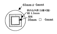
5mmtのホルダを準備した。ホルダ材はモリブデンとし、鏡面研磨加工によりRa:0.01μmとした。図3に示す如く、基板近傍部分のホルダ上に幅1.5mmの分離可能な部分を作製した。
ホルダは5種類作製し、分離可能な部分にはそれぞれダイヤモンド、SiO2、SiN
、SiCを表面に蒸着したものと、表面に何も蒸着を行なわなかったものを作製した。それぞれのホルダを用いて、基板上へマイクロ波プラズマCVDによるエピタキシャル成長を行った。基板温度は1200℃、圧力50torrで実施した。導入したガスはメタン180sccm(standard cubiccm)、水素900sccmとした。50時間が経過したところで、成膜を一時停止し、ホルダの分離可能部分を交換し、更に50時間成膜を行い、計100時間の成膜を行なった。
[Example 4]
An artificial Ib type single crystal {100} substrate of 5 mmφ and thickness 1.2 mm is prepared, and 65 mmφ−
A 5 mmt holder was prepared. The holder material was molybdenum, and Ra: 0.01 μm by mirror polishing. As shown in FIG. 3, a separable portion having a width of 1.5 mm was produced on the holder in the vicinity of the substrate.
Five types of holders are prepared, and diamond, SiO 2 , SiN are provided in separable parts.
An SiC was vapor-deposited on the surface, and no SiC was vapor-deposited on the surface. Using each holder, epitaxial growth by microwave plasma CVD was performed on the substrate. The substrate temperature was 1200 ° C. and the pressure was 50 torr. The introduced gas was methane 180 sccm (standard cubic cm) and hydrogen 900 sccm. When 50 hours had elapsed, the film formation was temporarily stopped, the separable part of the holder was replaced, and the film formation was further performed for 50 hours, for a total of 100 hours.
結果、ダイヤモンドが成膜したものではダイヤモンドの蒸着は見られたが剥離は起こらなかった。SiO2、SiN、SiCを成膜したものでは、ダイヤモンドの蒸着は見られ
なかった。表面に予め何も成膜を行なわなかったものは、40時間経過時に異常成長が発生し、これにより単結晶上のダイヤモンドは多結晶化してしまった。
As a result, diamond was deposited on the diamond film, but no peeling occurred. In the case of depositing SiO 2 , SiN, or SiC, diamond deposition was not observed. In the case where no film was formed on the surface in advance, abnormal growth occurred after 40 hours, and the diamond on the single crystal was polycrystallized.
Claims (10)
Priority Applications (1)
| Application Number | Priority Date | Filing Date | Title |
|---|---|---|---|
| JP2007175772A JP2009013003A (en) | 2007-07-04 | 2007-07-04 | Diamond manufacturing method and manufacturing apparatus |
Applications Claiming Priority (1)
| Application Number | Priority Date | Filing Date | Title |
|---|---|---|---|
| JP2007175772A JP2009013003A (en) | 2007-07-04 | 2007-07-04 | Diamond manufacturing method and manufacturing apparatus |
Publications (1)
| Publication Number | Publication Date |
|---|---|
| JP2009013003A true JP2009013003A (en) | 2009-01-22 |
Family
ID=40354360
Family Applications (1)
| Application Number | Title | Priority Date | Filing Date |
|---|---|---|---|
| JP2007175772A Pending JP2009013003A (en) | 2007-07-04 | 2007-07-04 | Diamond manufacturing method and manufacturing apparatus |
Country Status (1)
| Country | Link |
|---|---|
| JP (1) | JP2009013003A (en) |
Cited By (1)
| Publication number | Priority date | Publication date | Assignee | Title |
|---|---|---|---|---|
| CN112831835A (en) * | 2021-02-25 | 2021-05-25 | 廊坊西波尔钻石技术有限公司 | Substrate table structure for diamond growth and use method thereof |
-
2007
- 2007-07-04 JP JP2007175772A patent/JP2009013003A/en active Pending
Cited By (2)
| Publication number | Priority date | Publication date | Assignee | Title |
|---|---|---|---|---|
| CN112831835A (en) * | 2021-02-25 | 2021-05-25 | 廊坊西波尔钻石技术有限公司 | Substrate table structure for diamond growth and use method thereof |
| CN112831835B (en) * | 2021-02-25 | 2023-09-05 | 廊坊西波尔钻石技术有限公司 | Substrate table structure for diamond growth and use method thereof |
Similar Documents
| Publication | Publication Date | Title |
|---|---|---|
| US9200379B2 (en) | Base material for growing single crystal diamond and method for producing single crystal diamond substrate | |
| CN108400157B (en) | Base substrate for diamond film formation, and method for manufacturing diamond substrate using same | |
| US20110081531A1 (en) | Base material for growing single crystal diamond and method for producing single crystal diamond substrate | |
| KR102106424B1 (en) | Diamond substrate and diamond substrate manufacturing method | |
| TWI718800B (en) | Method of diamond nucleation and structure formed thereof | |
| JP5507888B2 (en) | Single crystal diamond layer growth substrate and method for manufacturing single crystal diamond substrate | |
| WO2004104272A1 (en) | Diamond-coated electrode and method for producing same | |
| JP6450920B2 (en) | Diamond substrate and method for manufacturing diamond substrate | |
| CN103649385A (en) | SiC epitaxial wafer and method for producing same, and device for producing SiC epitaxial wafer | |
| JP2011018772A (en) | Susceptor for silicon carbide single crystal film forming device | |
| CN106811737A (en) | A kind of base station component for preparing diamond | |
| JP5910430B2 (en) | Method for manufacturing epitaxial silicon carbide wafer | |
| JP4631499B2 (en) | Diamond substrate and manufacturing method thereof | |
| JP5085572B2 (en) | DC plasma CVD apparatus and method for producing diamond using the same | |
| JP2003051485A (en) | Coated silicon electrode plate for plasma etching | |
| JP5545567B2 (en) | Base material for single crystal diamond growth and method for producing single crystal diamond | |
| JP2017017084A (en) | Method for manufacturing silicon carbide epitaxial substrate and epitaxial growth apparatus | |
| JP2009013003A (en) | Diamond manufacturing method and manufacturing apparatus | |
| JP2020059648A (en) | Diamond substrate and method for manufacturing diamond substrate | |
| JP5867913B2 (en) | Silicon carbide film CVD system | |
| JP2005320208A (en) | Carbon composite member | |
| JP2012015229A (en) | Method of producing silicon carbide semiconductor device | |
| KR102207607B1 (en) | DC power plasma CVD diamond growth apparatus | |
| TW202543958A (en) | Composite substrate and device | |
| CN121472827A (en) | Manufacturing process of a multi-heat dissipation pedestal structure for MPCVD diamond growth |