JP2009016868A - リソグラフィ装置およびデバイス製造方法 - Google Patents
リソグラフィ装置およびデバイス製造方法 Download PDFInfo
- Publication number
- JP2009016868A JP2009016868A JP2008251029A JP2008251029A JP2009016868A JP 2009016868 A JP2009016868 A JP 2009016868A JP 2008251029 A JP2008251029 A JP 2008251029A JP 2008251029 A JP2008251029 A JP 2008251029A JP 2009016868 A JP2009016868 A JP 2009016868A
- Authority
- JP
- Japan
- Prior art keywords
- reference frame
- lithographic apparatus
- temperature
- substrate
- projection
- Prior art date
- Legal status (The legal status is an assumption and is not a legal conclusion. Google has not performed a legal analysis and makes no representation as to the accuracy of the status listed.)
- Granted
Links
- 238000004519 manufacturing process Methods 0.000 title claims description 14
- 239000000758 substrate Substances 0.000 claims abstract description 74
- 239000000463 material Substances 0.000 claims abstract description 48
- 230000005855 radiation Effects 0.000 claims description 33
- 238000005259 measurement Methods 0.000 claims description 24
- 238000012546 transfer Methods 0.000 claims description 24
- 230000003750 conditioning effect Effects 0.000 claims description 21
- 238000002955 isolation Methods 0.000 claims description 16
- 238000000059 patterning Methods 0.000 claims description 16
- 229910052782 aluminium Inorganic materials 0.000 claims description 15
- XAGFODPZIPBFFR-UHFFFAOYSA-N aluminium Chemical compound [Al] XAGFODPZIPBFFR-UHFFFAOYSA-N 0.000 claims description 15
- 230000007613 environmental effect Effects 0.000 claims description 15
- 230000001105 regulatory effect Effects 0.000 claims description 15
- 230000007774 longterm Effects 0.000 claims description 14
- 239000012530 fluid Substances 0.000 claims description 10
- 230000001276 controlling effect Effects 0.000 claims description 9
- XEEYBQQBJWHFJM-UHFFFAOYSA-N Iron Chemical compound [Fe] XEEYBQQBJWHFJM-UHFFFAOYSA-N 0.000 claims description 8
- 238000005286 illumination Methods 0.000 claims description 8
- 239000007787 solid Substances 0.000 claims description 8
- 229910000838 Al alloy Inorganic materials 0.000 claims description 7
- PXHVJJICTQNCMI-UHFFFAOYSA-N Nickel Chemical compound [Ni] PXHVJJICTQNCMI-UHFFFAOYSA-N 0.000 claims description 6
- 229910052742 iron Inorganic materials 0.000 claims description 4
- 239000010935 stainless steel Substances 0.000 claims description 4
- 229910001220 stainless steel Inorganic materials 0.000 claims description 4
- 229910001018 Cast iron Inorganic materials 0.000 claims description 3
- RYGMFSIKBFXOCR-UHFFFAOYSA-N Copper Chemical compound [Cu] RYGMFSIKBFXOCR-UHFFFAOYSA-N 0.000 claims description 3
- 229910000831 Steel Inorganic materials 0.000 claims description 3
- RTAQQCXQSZGOHL-UHFFFAOYSA-N Titanium Chemical compound [Ti] RTAQQCXQSZGOHL-UHFFFAOYSA-N 0.000 claims description 3
- 229910010293 ceramic material Inorganic materials 0.000 claims description 3
- 239000002131 composite material Substances 0.000 claims description 3
- 239000004567 concrete Substances 0.000 claims description 3
- 229910052802 copper Inorganic materials 0.000 claims description 3
- 239000010949 copper Substances 0.000 claims description 3
- 239000010438 granite Substances 0.000 claims description 3
- 229910052759 nickel Inorganic materials 0.000 claims description 3
- 229910052573 porcelain Inorganic materials 0.000 claims description 3
- 239000010959 steel Substances 0.000 claims description 3
- 239000010936 titanium Substances 0.000 claims description 3
- 229910052719 titanium Inorganic materials 0.000 claims description 3
- 229910052751 metal Inorganic materials 0.000 claims 2
- 239000002184 metal Substances 0.000 claims 2
- 238000001816 cooling Methods 0.000 description 17
- 239000003570 air Substances 0.000 description 13
- 230000003287 optical effect Effects 0.000 description 9
- XLYOFNOQVPJJNP-UHFFFAOYSA-N water Substances O XLYOFNOQVPJJNP-UHFFFAOYSA-N 0.000 description 9
- 239000011248 coating agent Substances 0.000 description 6
- 238000000576 coating method Methods 0.000 description 6
- 230000006870 function Effects 0.000 description 6
- 230000002829 reductive effect Effects 0.000 description 5
- 239000000956 alloy Substances 0.000 description 4
- 230000008901 benefit Effects 0.000 description 4
- 230000033228 biological regulation Effects 0.000 description 4
- 230000000694 effects Effects 0.000 description 4
- 239000010410 layer Substances 0.000 description 4
- 230000033001 locomotion Effects 0.000 description 4
- 229910045601 alloy Inorganic materials 0.000 description 3
- 238000013461 design Methods 0.000 description 3
- 238000009826 distribution Methods 0.000 description 3
- 238000003384 imaging method Methods 0.000 description 3
- 238000007654 immersion Methods 0.000 description 3
- 238000001459 lithography Methods 0.000 description 3
- 238000000034 method Methods 0.000 description 3
- 239000000110 cooling liquid Substances 0.000 description 2
- 239000000498 cooling water Substances 0.000 description 2
- 230000009977 dual effect Effects 0.000 description 2
- 238000009434 installation Methods 0.000 description 2
- 239000007788 liquid Substances 0.000 description 2
- 238000012423 maintenance Methods 0.000 description 2
- 239000007769 metal material Substances 0.000 description 2
- 230000010363 phase shift Effects 0.000 description 2
- 238000012545 processing Methods 0.000 description 2
- 230000008439 repair process Effects 0.000 description 2
- 230000003068 static effect Effects 0.000 description 2
- XUIMIQQOPSSXEZ-UHFFFAOYSA-N Silicon Chemical compound [Si] XUIMIQQOPSSXEZ-UHFFFAOYSA-N 0.000 description 1
- 230000002411 adverse Effects 0.000 description 1
- 239000012080 ambient air Substances 0.000 description 1
- 238000003491 array Methods 0.000 description 1
- 238000000429 assembly Methods 0.000 description 1
- 230000000712 assembly Effects 0.000 description 1
- 230000002238 attenuated effect Effects 0.000 description 1
- 238000005266 casting Methods 0.000 description 1
- 230000001143 conditioned effect Effects 0.000 description 1
- 238000011109 contamination Methods 0.000 description 1
- 239000012809 cooling fluid Substances 0.000 description 1
- 238000012937 correction Methods 0.000 description 1
- 230000003247 decreasing effect Effects 0.000 description 1
- 238000001514 detection method Methods 0.000 description 1
- 238000011161 development Methods 0.000 description 1
- 230000005670 electromagnetic radiation Effects 0.000 description 1
- 238000010894 electron beam technology Methods 0.000 description 1
- -1 for example Substances 0.000 description 1
- 230000005484 gravity Effects 0.000 description 1
- 238000010438 heat treatment Methods 0.000 description 1
- 238000007689 inspection Methods 0.000 description 1
- 238000009413 insulation Methods 0.000 description 1
- 238000010884 ion-beam technique Methods 0.000 description 1
- 239000002346 layers by function Substances 0.000 description 1
- 239000004973 liquid crystal related substance Substances 0.000 description 1
- 238000003754 machining Methods 0.000 description 1
- 239000011159 matrix material Substances 0.000 description 1
- QSHDDOUJBYECFT-UHFFFAOYSA-N mercury Chemical compound [Hg] QSHDDOUJBYECFT-UHFFFAOYSA-N 0.000 description 1
- 229910052753 mercury Inorganic materials 0.000 description 1
- 238000012986 modification Methods 0.000 description 1
- 230000004048 modification Effects 0.000 description 1
- 239000002245 particle Substances 0.000 description 1
- 238000005498 polishing Methods 0.000 description 1
- 210000001747 pupil Anatomy 0.000 description 1
- 238000011084 recovery Methods 0.000 description 1
- 230000009467 reduction Effects 0.000 description 1
- 238000007493 shaping process Methods 0.000 description 1
- 229910052710 silicon Inorganic materials 0.000 description 1
- 239000010703 silicon Substances 0.000 description 1
- 230000006641 stabilisation Effects 0.000 description 1
- 238000011105 stabilization Methods 0.000 description 1
- 239000010409 thin film Substances 0.000 description 1
- 238000011144 upstream manufacturing Methods 0.000 description 1
- 238000003466 welding Methods 0.000 description 1
Images



Classifications
-
- G—PHYSICS
- G03—PHOTOGRAPHY; CINEMATOGRAPHY; ANALOGOUS TECHNIQUES USING WAVES OTHER THAN OPTICAL WAVES; ELECTROGRAPHY; HOLOGRAPHY
- G03F—PHOTOMECHANICAL PRODUCTION OF TEXTURED OR PATTERNED SURFACES, e.g. FOR PRINTING, FOR PROCESSING OF SEMICONDUCTOR DEVICES; MATERIALS THEREFOR; ORIGINALS THEREFOR; APPARATUS SPECIALLY ADAPTED THEREFOR
- G03F7/00—Photomechanical, e.g. photolithographic, production of textured or patterned surfaces, e.g. printing surfaces; Materials therefor, e.g. comprising photoresists; Apparatus specially adapted therefor
- G03F7/70—Microphotolithographic exposure; Apparatus therefor
- G03F7/708—Construction of apparatus, e.g. environment aspects, hygiene aspects or materials
- G03F7/70808—Construction details, e.g. housing, load-lock, seals or windows for passing light in or out of apparatus
- G03F7/70825—Mounting of individual elements, e.g. mounts, holders or supports
-
- G—PHYSICS
- G02—OPTICS
- G02B—OPTICAL ELEMENTS, SYSTEMS OR APPARATUS
- G02B7/00—Mountings, adjusting means, or light-tight connections, for optical elements
- G02B7/02—Mountings, adjusting means, or light-tight connections, for optical elements for lenses
- G02B7/028—Mountings, adjusting means, or light-tight connections, for optical elements for lenses with means for compensating for changes in temperature or for controlling the temperature; thermal stabilisation
-
- G—PHYSICS
- G03—PHOTOGRAPHY; CINEMATOGRAPHY; ANALOGOUS TECHNIQUES USING WAVES OTHER THAN OPTICAL WAVES; ELECTROGRAPHY; HOLOGRAPHY
- G03F—PHOTOMECHANICAL PRODUCTION OF TEXTURED OR PATTERNED SURFACES, e.g. FOR PRINTING, FOR PROCESSING OF SEMICONDUCTOR DEVICES; MATERIALS THEREFOR; ORIGINALS THEREFOR; APPARATUS SPECIALLY ADAPTED THEREFOR
- G03F7/00—Photomechanical, e.g. photolithographic, production of textured or patterned surfaces, e.g. printing surfaces; Materials therefor, e.g. comprising photoresists; Apparatus specially adapted therefor
- G03F7/70—Microphotolithographic exposure; Apparatus therefor
- G03F7/708—Construction of apparatus, e.g. environment aspects, hygiene aspects or materials
- G03F7/70808—Construction details, e.g. housing, load-lock, seals or windows for passing light in or out of apparatus
- G03F7/70833—Mounting of optical systems, e.g. mounting of illumination system, projection system or stage systems on base-plate or ground
-
- G—PHYSICS
- G03—PHOTOGRAPHY; CINEMATOGRAPHY; ANALOGOUS TECHNIQUES USING WAVES OTHER THAN OPTICAL WAVES; ELECTROGRAPHY; HOLOGRAPHY
- G03F—PHOTOMECHANICAL PRODUCTION OF TEXTURED OR PATTERNED SURFACES, e.g. FOR PRINTING, FOR PROCESSING OF SEMICONDUCTOR DEVICES; MATERIALS THEREFOR; ORIGINALS THEREFOR; APPARATUS SPECIALLY ADAPTED THEREFOR
- G03F7/00—Photomechanical, e.g. photolithographic, production of textured or patterned surfaces, e.g. printing surfaces; Materials therefor, e.g. comprising photoresists; Apparatus specially adapted therefor
- G03F7/70—Microphotolithographic exposure; Apparatus therefor
- G03F7/708—Construction of apparatus, e.g. environment aspects, hygiene aspects or materials
- G03F7/70858—Environment aspects, e.g. pressure of beam-path gas, temperature
-
- G—PHYSICS
- G03—PHOTOGRAPHY; CINEMATOGRAPHY; ANALOGOUS TECHNIQUES USING WAVES OTHER THAN OPTICAL WAVES; ELECTROGRAPHY; HOLOGRAPHY
- G03F—PHOTOMECHANICAL PRODUCTION OF TEXTURED OR PATTERNED SURFACES, e.g. FOR PRINTING, FOR PROCESSING OF SEMICONDUCTOR DEVICES; MATERIALS THEREFOR; ORIGINALS THEREFOR; APPARATUS SPECIALLY ADAPTED THEREFOR
- G03F7/00—Photomechanical, e.g. photolithographic, production of textured or patterned surfaces, e.g. printing surfaces; Materials therefor, e.g. comprising photoresists; Apparatus specially adapted therefor
- G03F7/70—Microphotolithographic exposure; Apparatus therefor
- G03F7/708—Construction of apparatus, e.g. environment aspects, hygiene aspects or materials
- G03F7/70858—Environment aspects, e.g. pressure of beam-path gas, temperature
- G03F7/709—Vibration, e.g. vibration detection, compensation, suppression or isolation
-
- G—PHYSICS
- G03—PHOTOGRAPHY; CINEMATOGRAPHY; ANALOGOUS TECHNIQUES USING WAVES OTHER THAN OPTICAL WAVES; ELECTROGRAPHY; HOLOGRAPHY
- G03F—PHOTOMECHANICAL PRODUCTION OF TEXTURED OR PATTERNED SURFACES, e.g. FOR PRINTING, FOR PROCESSING OF SEMICONDUCTOR DEVICES; MATERIALS THEREFOR; ORIGINALS THEREFOR; APPARATUS SPECIALLY ADAPTED THEREFOR
- G03F7/00—Photomechanical, e.g. photolithographic, production of textured or patterned surfaces, e.g. printing surfaces; Materials therefor, e.g. comprising photoresists; Apparatus specially adapted therefor
- G03F7/70—Microphotolithographic exposure; Apparatus therefor
- G03F7/708—Construction of apparatus, e.g. environment aspects, hygiene aspects or materials
- G03F7/7095—Materials, e.g. materials for housing, stage or other support having particular properties, e.g. weight, strength, conductivity, thermal expansion coefficient
-
- G—PHYSICS
- G03—PHOTOGRAPHY; CINEMATOGRAPHY; ANALOGOUS TECHNIQUES USING WAVES OTHER THAN OPTICAL WAVES; ELECTROGRAPHY; HOLOGRAPHY
- G03F—PHOTOMECHANICAL PRODUCTION OF TEXTURED OR PATTERNED SURFACES, e.g. FOR PRINTING, FOR PROCESSING OF SEMICONDUCTOR DEVICES; MATERIALS THEREFOR; ORIGINALS THEREFOR; APPARATUS SPECIALLY ADAPTED THEREFOR
- G03F7/00—Photomechanical, e.g. photolithographic, production of textured or patterned surfaces, e.g. printing surfaces; Materials therefor, e.g. comprising photoresists; Apparatus specially adapted therefor
- G03F7/70—Microphotolithographic exposure; Apparatus therefor
- G03F7/708—Construction of apparatus, e.g. environment aspects, hygiene aspects or materials
- G03F7/70991—Connection with other apparatus, e.g. multiple exposure stations, particular arrangement of exposure apparatus and pre-exposure and/or post-exposure apparatus; Shared apparatus, e.g. having shared radiation source, shared mask or workpiece stage, shared base-plate; Utilities, e.g. cable, pipe or wireless arrangements for data, power, fluids or vacuum
Landscapes
- Physics & Mathematics (AREA)
- Health & Medical Sciences (AREA)
- General Physics & Mathematics (AREA)
- Engineering & Computer Science (AREA)
- Environmental & Geological Engineering (AREA)
- Public Health (AREA)
- Epidemiology (AREA)
- Life Sciences & Earth Sciences (AREA)
- Atmospheric Sciences (AREA)
- Toxicology (AREA)
- Optics & Photonics (AREA)
- Computer Networks & Wireless Communication (AREA)
- Exposure And Positioning Against Photoresist Photosensitive Materials (AREA)
- Exposure Of Semiconductors, Excluding Electron Or Ion Beam Exposure (AREA)
- Container, Conveyance, Adherence, Positioning, Of Wafer (AREA)
Abstract
【解決手段】基板Wを保持するための基板テーブルWT、基板Wの目標部分上にパターン化されたビームを投影するための投影システムPL、および基板Wが測定される基準面を供給するための独立基準フレームMFを備えるリソグラフィ装置。基準フレームMFは熱膨張係数の大きい材料を含有する。
【選択図】図3
Description
放射線の投影ビームを供給するための照明システムと、
投影ビームにあるパターンの断面の形を与える働きをするパターニング手段を支持するための支持構造と、
基板を保持するための基板テーブルと、
基板の目標部分上にパターン化されたビームを投影するための投影システムと、
上記基板を測定するための基準面を供給する独立基準フレームとを備え、
上記基準フレームが、熱膨張係数の大きい材料を含有することを特徴とするリソグラフィ装置を提供する。
基板を供給するステップと、
照明システムにより放射線のビームを投影するステップと、
投影ビームにあるパターンの断面を与えるためにパターニング手段を使用するステップと、
基板の目標部分上に放射線のパターン化されたビームを投影するステップと、
上記基板を測定するための基準面を供給するために、独立基準フレームを使用するステップとを含み、上記基準フレームが、高い熱膨張係数を有する材料を含有することを特徴とするデバイス製造方法を提供する。
放射線(例えば、UV放射線またはEUV放射線)の投影ビームPBを供給するための照明システム(照明装置)ILと、
パターニング手段(例えば、マスク)MAを支持し、品目PLに対してパターニング手段を正確に位置決めするために、第1の位置決め手段PMに接続している第1の支持構造(例えば、マスク・テーブル)MTと、
基板(例えば、レジストでコーティングされたウェハ)Wを保持し、品目PLに対して基板を正確に位置決めするために第2の位置決め手段PWに接続している基板テーブル(例えば、ウェハ・テーブル)WTと、
基板Wの目標部分C(例えば、1つまたはそれ以上のダイを備える)上にパターニング手段MAにより、投影ビームPBに与えられた形をしているパターンを画像形成するための投影システム(例えば、屈折投影レンズ)PLとを備える。
1.ステップ・モードの場合には、マスク・テーブルMTおよび基板テーブルWTは本質的に固定されていて、一方、投影ビームに与えられた全パターンが、1回で(すなわち、1回の静的露光で)目標部分C上に投影される。基板テーブルWTは、次に、Xおよび/またはY方向にシフトされ、そのため異なる目標部分Cを露光することができる。ステップ・モードの場合には、露光フィールドの最大サイズにより1回の静的露光で画像形成される目標部分Cのサイズが制限される。
2.走査モードの場合、マスク・テーブルMTおよび基板テーブルWTは同期状態で走査され、一方、投影ビームに与えられたパターンが、目標部分C上に投影される(すなわち、1回の動的露光)。マスク・テーブルMTに対する基板テーブルWTの速度および方向は、倍率(縮少率)および投影システムPLの画像の逆特性により決まる。走査モードの場合には、露光フィールドの最大サイズにより1回の動的露光の際の目標部分の(走査方向でない方向の)幅が制限され、一方、走査運動の長さにより目標部分の(走査方向の)高さが決まる。

IL 照明システム
MA マスク
PM 第1の位置決め手段
MT 第1の支持構造
W 基板
PW 第2の位置決め手段
WT 基板テーブル
C 目標部分
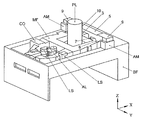
PL 投影システム
SO 放射線源
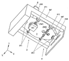
IF 干渉計
M1,M2 マスク整合マーク
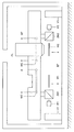
MF 基準フレーム
BF ベース・フレーム
ZM1 第1のZミラー
LS レベル・センサ・モジュール
2 測定ステーション
4 露光ステーション
6 入口
8 出口
10 延長部分
20 制御回路2
21,22 温度センサ
28,30,32,34,36,38 熱移送システム
60,61,63 トレース
Claims (27)
- 放射ビームを調整する照明システムと、
放射ビームの断面にパターンを与えるパターニングデバイスを支持する支持部と、
基板を保持する基板テーブルと、
パターンが与えられたビームを基板の目標部分に投影する投影システムと、
基準面を有する独立基準フレームと、
前記基準面に対する基板の少なくとも1つの寸法を測定する測定システムと、を備え、
前記基準フレームは、熱膨張係数が約2.9×10⁻⁶/Kより大きい材料を含むことを特徴とするリソグラフィ装置。 - 前記基準フレームは、基板の少なくとも1つの寸法をその露光前に測定する測定システムを支持することを特徴とする請求項1に記載のリソグラフィ装置。
- 前記基準フレームは、前記投影システムを支持することを特徴とする請求項1に記載のリソグラフィ装置。
- 前記基準フレームは、アルミニウム、アルミニウム合金、チタン、鉄、鋳鉄、鋼鉄、ステンレス鋼、銅、セラミック材料、コンクリート、花崗岩、磁器からなるグループのうち少なくとも1つの材料を含むことを特徴とする請求項1に記載のリソグラフィ装置。
- 前記基準フレームは、複合構造、サンドイッチ構造、または積層構造を備えることを特徴とする請求項4に記載のリソグラフィ装置。
- 前記基準フレームは、材料の中実ブロックを備えることを特徴とする請求項1に記載のリソグラフィ装置。
- 前記中実ブロックは、機械加工されて前記基準フレームを形成していることを特徴とする請求項6に記載のリソグラフィ装置。
- 前記基準フレームは、第1および第2の部分を備えることを特徴とする請求項7に記載のリソグラフィ装置。
- リソグラフィ装置で生じた振動から前記第1および第2の部分の少なくとも一方を絶縁するよう前記第1および第2の部分の少なくとも一方のために設けられている振動絶縁システムをさらに備えることを特徴とする請求項8に記載のリソグラフィ装置。
- 前記基準フレームは、前記基準フレームに対する前記投影システムの温度を制御する熱調整システムを備えることを特徴とする請求項1に記載のリソグラフィ装置。
- 前記熱調整システムは、基準フレームおよび投影レンズを調整流体により調整することを特徴とする請求項10に記載のリソグラフィ装置。
- 前記基準フレームは、赤外線をよく反射する面を備えることを特徴とする請求項1に記載のリソグラフィ装置。
- 前記面は金属でコーティングされていることを特徴とする請求項12に記載のリソグラフィ装置。
- 前記金属はニッケルを含むことを特徴とする請求項13に記載のリソグラフィ装置。
- 前記基準フレームは、比熱が約600J/(kgK)より大きい材料および/または熱伝導性が約20W/(mK)より高い材料で形成されていることを特徴とする請求項1に記載のリソグラフィ装置。
- リソグラフィ装置で生じた振動から前記基準フレームを絶縁するよう前記基準フレームのために設けられている振動絶縁システムをさらに備えることを特徴とする請求項1に記載のリソグラフィ装置。
- 前記振動絶縁システムを支持するベース・フレームをさらに備えることを特徴とする請求項9に記載のリソグラフィ装置。
- 前記基準フレームの温度を測定する第1の温度センサをさらに備えることを特徴とする請求項1に記載のリソグラフィ装置。
- 前記投影システムは投影レンズを備え、
前記投影レンズの温度を測定する第2の温度センサをさらに備えることを特徴とする請求項18に記載のリソグラフィ装置。 - 前記第1及び/または第2の温度センサにより測定された温度に基づいて前記基準フレーム及び/または前記投影システムを熱的に調整する熱調整システムをさらに備えることを特徴とする請求項19に記載のリソグラフィ装置。
- 前記熱調整システムは、
前記基準フレーム及び/または投影レンズに流入または流出する熱量を制御する制御回路と、
温度規制素子と、
熱移送システムと、を備え、
前記温度規制素子は前記熱移送システムが移送する熱量を規制し、前記熱移送システムは前記基準フレーム及び/または前記投影レンズに熱を流入または流出させるよう前記基準フレーム及び/または前記投影レンズと熱的に接触しており、前記制御回路は前記第1及び/または第2の温度センサにより測定された温度に応答可能であり、前記温度規制素子は前記制御回路に応答可能でありかつ前記熱移送システムに熱的に接触していることにより、前記基準フレーム及び/または前記投影レンズを設定温度に到達させることを特徴とする請求項20に記載のリソグラフィ装置。 - 前記制御回路は、前記第1の温度センサが測定した温度を考慮に入れて環境温度の短期変動を補償することを特徴とする請求項21に記載のリソグラフィ装置。
- 前記制御回路は、前記第2の温度センサが測定した温度を考慮に入れて環境温度の長期変動を補償することを特徴とする請求項21に記載のリソグラフィ装置。
- 前記熱調整システムは、前記基準フレームおよび前記投影レンズの温度を制御する1つの制御ループを備えることを特徴とする請求項21に記載のリソグラフィ装置。
- 前記熱移送システムは、前記設定温度に加熱または冷却される調整流体を備えることを特徴とする請求項21に記載のリソグラフィ装置。
- 前記投影システムと前記基板との間のある位置にガスを供給するためのガス供給源をさらに備え、前記位置に供給されるガスの温度が前記調整流体の温度によって決定されることを特徴とする請求項21に記載のリソグラフィ装置。
- 放射ビームを調整し、
放射ビームにパターンを付与し、
パターンが付与された放射ビームを基板の目標部分に投影し、
熱膨張係数が約2.9×10⁻⁶/Kより大きい材料を含む独立基準フレームを基準面を与えるように使用し、
前記基準面に対する基板の少なくとも1つの寸法を測定することを含むことを特徴とするデバイス製造方法。
Applications Claiming Priority (4)
| Application Number | Priority Date | Filing Date | Title |
|---|---|---|---|
| US735847 | 1985-05-20 | ||
| NLPCT/NL03/00798 | 2003-11-13 | ||
| NL0300798 | 2003-11-13 | ||
| US10/735,847 US7061579B2 (en) | 2003-11-13 | 2003-12-16 | Lithographic apparatus and device manufacturing method |
Related Parent Applications (1)
| Application Number | Title | Priority Date | Filing Date |
|---|---|---|---|
| JP2004328305A Division JP4452160B2 (ja) | 2003-11-13 | 2004-11-12 | リソグラフィ装置およびデバイス製造方法 |
Related Child Applications (1)
| Application Number | Title | Priority Date | Filing Date |
|---|---|---|---|
| JP2011199359A Division JP5619699B2 (ja) | 2003-11-13 | 2011-09-13 | リソグラフィ装置、フレームシステム、およびデバイス製造方法 |
Publications (2)
| Publication Number | Publication Date |
|---|---|
| JP2009016868A true JP2009016868A (ja) | 2009-01-22 |
| JP4900970B2 JP4900970B2 (ja) | 2012-03-21 |
Family
ID=34437049
Family Applications (3)
| Application Number | Title | Priority Date | Filing Date |
|---|---|---|---|
| JP2004328305A Expired - Fee Related JP4452160B2 (ja) | 2003-11-13 | 2004-11-12 | リソグラフィ装置およびデバイス製造方法 |
| JP2008251029A Expired - Fee Related JP4900970B2 (ja) | 2003-11-13 | 2008-09-29 | リソグラフィ装置およびデバイス製造方法 |
| JP2011199359A Expired - Fee Related JP5619699B2 (ja) | 2003-11-13 | 2011-09-13 | リソグラフィ装置、フレームシステム、およびデバイス製造方法 |
Family Applications Before (1)
| Application Number | Title | Priority Date | Filing Date |
|---|---|---|---|
| JP2004328305A Expired - Fee Related JP4452160B2 (ja) | 2003-11-13 | 2004-11-12 | リソグラフィ装置およびデバイス製造方法 |
Family Applications After (1)
| Application Number | Title | Priority Date | Filing Date |
|---|---|---|---|
| JP2011199359A Expired - Fee Related JP5619699B2 (ja) | 2003-11-13 | 2011-09-13 | リソグラフィ装置、フレームシステム、およびデバイス製造方法 |
Country Status (7)
| Country | Link |
|---|---|
| US (2) | US7061579B2 (ja) |
| EP (1) | EP1531364B1 (ja) |
| JP (3) | JP4452160B2 (ja) |
| KR (1) | KR100632424B1 (ja) |
| CN (1) | CN100595674C (ja) |
| SG (1) | SG112064A1 (ja) |
| TW (1) | TWI251131B (ja) |
Families Citing this family (31)
| Publication number | Priority date | Publication date | Assignee | Title |
|---|---|---|---|---|
| US6977713B2 (en) * | 2003-12-08 | 2005-12-20 | Asml Netherlands B.V. | Lithographic apparatus and device manufacturing method |
| JP4371822B2 (ja) * | 2004-01-06 | 2009-11-25 | キヤノン株式会社 | 露光装置 |
| JP4429023B2 (ja) * | 2004-01-07 | 2010-03-10 | キヤノン株式会社 | 露光装置及びデバイス製造方法 |
| CN1938646B (zh) | 2004-01-20 | 2010-12-15 | 卡尔蔡司Smt股份公司 | 曝光装置和用于投影透镜的测量装置 |
| EP1898241A4 (en) * | 2005-06-14 | 2010-11-03 | Nikon Corp | OPTICAL ELEMENT, OPTICAL ELEMENT SUPPORT APPARATUS, EXPOSURE APPARATUS, AND DEVICE MANUFACTURING METHOD |
| KR100647517B1 (ko) | 2005-08-26 | 2006-11-23 | (주)마스터이미지 | 셀 구조 패러랙스-배리어 및 이를 이용하는 입체영상 표시장치 |
| JP2009517627A (ja) * | 2005-11-30 | 2009-04-30 | コーニンクレッカ フィリップス エレクトロニクス エヌ ヴィ | 機械温度をより正確に調節するための熱流の局部的制御 |
| US20070185216A1 (en) | 2006-02-09 | 2007-08-09 | Marcia Snyder | Antiviral method |
| JP4315455B2 (ja) | 2006-04-04 | 2009-08-19 | キヤノン株式会社 | 露光装置及びデバイス製造方法 |
| DE102006021797A1 (de) * | 2006-05-09 | 2007-11-15 | Carl Zeiss Smt Ag | Optische Abbildungseinrichtung mit thermischer Dämpfung |
| US8760621B2 (en) * | 2007-03-12 | 2014-06-24 | Asml Netherlands B.V. | Lithographic apparatus and method |
| US7804579B2 (en) * | 2007-06-21 | 2010-09-28 | Asml Netherlands B.V. | Control system, lithographic projection apparatus, method of controlling a support structure, and a computer program product |
| WO2009046955A2 (en) | 2007-10-09 | 2009-04-16 | Carl Zeiss Smt Ag | Device for controlling temperature of an optical element |
| KR101768983B1 (ko) | 2008-06-10 | 2017-08-17 | 에이에스엠엘 네델란즈 비.브이. | 광학 요소를 열적으로 컨디셔닝하는 방법 및 시스템 |
| DE102009034166A1 (de) | 2008-08-11 | 2010-02-18 | Carl Zeiss Smt Ag | Kontaminationsarme optische Anordnung |
| WO2010037575A1 (en) | 2008-09-30 | 2010-04-08 | Asml Netherlands B.V. | Projection system and lithographic apparatus |
| JP5783811B2 (ja) * | 2010-07-06 | 2015-09-24 | キヤノン株式会社 | 成膜装置 |
| CN102841507B (zh) * | 2011-06-23 | 2014-06-25 | 虎尾科技大学 | 激光直写式纳米周期性结构图案制造设备 |
| DE102011114254B4 (de) * | 2011-09-26 | 2014-11-27 | Carl Zeiss Smt Gmbh | Messvorrichtung und optisches System mit einer solchen |
| CN103324032B (zh) * | 2012-03-22 | 2015-07-22 | 上海微电子装备有限公司 | 一种多面体主基板及其制造方法和加工方法 |
| CN103777303B (zh) * | 2012-10-19 | 2016-02-03 | 上海微电子装备有限公司 | 长条镜安装装置 |
| KR102388549B1 (ko) * | 2014-09-15 | 2022-04-20 | 칼 짜이스 에스엠테 게엠베하 | 세라믹 구성요소의 논-포지티브 연결을 위한 연결 배열체 |
| DE102015211286A1 (de) * | 2015-06-18 | 2016-12-22 | Carl Zeiss Smt Gmbh | Abbildungssystem und verfahren |
| CN106931878A (zh) | 2015-12-31 | 2017-07-07 | 上海微电子装备有限公司 | 一种干涉仪测量装置及其控制方法 |
| CN109791380B (zh) * | 2016-10-04 | 2021-04-16 | Asml荷兰有限公司 | 对准系统的无热化 |
| DE102018201320A1 (de) | 2018-01-29 | 2019-08-01 | Carl Zeiss Smt Gmbh | Verfahren zum Temperieren einer Komponente |
| WO2019081187A1 (en) | 2017-10-25 | 2019-05-02 | Carl Zeiss Smt Gmbh | METHOD FOR REGULATING THE TEMPERATURE OF A COMPONENT |
| DE102017219151A1 (de) | 2017-10-25 | 2019-04-25 | Carl Zeiss Smt Gmbh | Verfahren zum Temperieren einer Komponente |
| CN109856921A (zh) * | 2017-11-30 | 2019-06-07 | 上海微电子装备(集团)股份有限公司 | 光刻装置及其主基板结构与主基板单元 |
| WO2020164868A1 (en) * | 2019-02-11 | 2020-08-20 | Asml Netherlands B.V. | Lithographic apparatus and method with a thermal control system |
| DE102021201258A1 (de) | 2021-02-10 | 2022-08-11 | Carl Zeiss Smt Gmbh | Verfahren zum Heizen eines optischen Elements in einer mikrolithographischen Projektionsbelichtungsanlage, sowie optisches System |
Citations (5)
| Publication number | Priority date | Publication date | Assignee | Title |
|---|---|---|---|---|
| JPH03198320A (ja) * | 1989-12-27 | 1991-08-29 | Nikon Corp | 投影光学装置 |
| JPH10303112A (ja) * | 1997-04-22 | 1998-11-13 | Canon Inc | 投影露光装置 |
| JP2001244178A (ja) * | 2000-02-29 | 2001-09-07 | Canon Inc | 露光装置および露光方法ならびにデバイス製造方法 |
| JP2002124461A (ja) * | 2000-08-03 | 2002-04-26 | Asm Lithography Bv | 平板投影装置、素子製造方法およびそれによって製造された素子 |
| JP2002190438A (ja) * | 2000-12-21 | 2002-07-05 | Nikon Corp | 露光装置 |
Family Cites Families (29)
| Publication number | Priority date | Publication date | Assignee | Title |
|---|---|---|---|---|
| US6020950A (en) * | 1992-02-24 | 2000-02-01 | Nikon Corporation | Exposure method and projection exposure apparatus |
| KR0139039B1 (ko) * | 1993-06-30 | 1998-06-01 | 미타라이 하지메 | 노광장치와 이것을 이용한 디바이스 제조방법 |
| US5953105A (en) * | 1995-05-30 | 1999-09-14 | U.S. Philips Corporation | Positioning device with a reference frame for a measuring system, and a lithographic device provided with such a positioning device |
| US5883704A (en) * | 1995-08-07 | 1999-03-16 | Nikon Corporation | Projection exposure apparatus wherein focusing of the apparatus is changed by controlling the temperature of a lens element of the projection optical system |
| US5877843A (en) * | 1995-09-12 | 1999-03-02 | Nikon Corporation | Exposure apparatus |
| US5644137A (en) * | 1996-03-04 | 1997-07-01 | Waggener; Herbert A. | Stabilizing support mechanism for electron beam apparatus |
| JPH10209040A (ja) * | 1996-11-25 | 1998-08-07 | Nikon Corp | 露光装置 |
| WO1998028665A1 (en) * | 1996-12-24 | 1998-07-02 | Koninklijke Philips Electronics N.V. | Two-dimensionally balanced positioning device with two object holders, and lithographic device provided with such a positioning device |
| KR100250152B1 (ko) * | 1997-11-15 | 2000-03-15 | 유무성 | 노광장치 |
| AU1260099A (en) | 1997-11-25 | 1999-06-15 | Nikon Corporation | Projection exposure system |
| AU1261699A (en) * | 1997-11-28 | 1999-06-16 | Nikon Corporation | Substrate retaining apparatus and exposure apparatus using the same |
| JPH11354431A (ja) * | 1998-06-11 | 1999-12-24 | Nikon Corp | 投影露光装置及び半導体デバイスの製造方法 |
| US6262795B1 (en) * | 1998-08-28 | 2001-07-17 | Philip Semiconductors, Inc. | Apparatus and method for the improvement of illumination uniformity in photolithographic systems |
| US6118599A (en) * | 1998-11-03 | 2000-09-12 | Nikon Corporation | Hybrid optical barrel |
| JP2001126977A (ja) * | 1999-10-27 | 2001-05-11 | Nikon Corp | ステージ装置および露光装置ならびに回路デバイス製造方法 |
| TWI231405B (en) * | 1999-12-22 | 2005-04-21 | Asml Netherlands Bv | Lithographic projection apparatus, position detection device, and method of manufacturing a device using a lithographic projection apparatus |
| US6621556B2 (en) * | 2000-02-28 | 2003-09-16 | Nikon Corporation | Projection exposure apparatus and manufacturing and adjusting methods thereof |
| EP1178357A1 (en) * | 2000-08-03 | 2002-02-06 | Asm Lithography B.V. | Lithographic apparatus |
| US6473245B1 (en) * | 2000-08-10 | 2002-10-29 | Nikon Corporation | Catadioptric lens barrel structure having a plurality of support platforms and method of making the same |
| US6577457B1 (en) * | 2000-08-10 | 2003-06-10 | Nikon Corporation | Catadioptric lens barrel structure having a kinematic alignment structure and method for aligning two planar surfaces |
| US6549347B1 (en) * | 2000-08-10 | 2003-04-15 | Nikon Corporation | Catadioptric lens barrel structure |
| US6449106B1 (en) * | 2000-08-10 | 2002-09-10 | Nikon Corporation | Catadioptric lens barrel structure having a support structure to maintain alignment of a plurality of sub-barrels |
| US6774981B1 (en) | 2000-09-08 | 2004-08-10 | Nikon Corporation | Modular exposure apparatus with removable optical device and improved isolation of the optical device |
| JP2002217095A (ja) * | 2000-11-14 | 2002-08-02 | Canon Inc | 露光装置、半導体デバイス製造方法、半導体製造工場及び露光装置の保守方法並びに位置検出装置 |
| US6538720B2 (en) * | 2001-02-28 | 2003-03-25 | Silicon Valley Group, Inc. | Lithographic tool with dual isolation system and method for configuring the same |
| US20020155364A1 (en) * | 2001-04-20 | 2002-10-24 | David Trost | Method and system to achieve thermal transfer between a workpiece and a heated body disposed in a chamber |
| US6674512B2 (en) * | 2001-08-07 | 2004-01-06 | Nikon Corporation | Interferometer system for a semiconductor exposure system |
| US6876452B2 (en) * | 2001-12-13 | 2005-04-05 | Zygo Corporation | Apparatus and methods for high accuracy metrology and positioning of a body |
| US20040204777A1 (en) * | 2003-04-14 | 2004-10-14 | Alon Harpaz | Precision motion control using feed forward of acceleration |
-
2003
- 2003-12-16 US US10/735,847 patent/US7061579B2/en not_active Expired - Lifetime
-
2004
- 2004-11-02 EP EP04078004.1A patent/EP1531364B1/en not_active Expired - Lifetime
- 2004-11-10 SG SG200406895A patent/SG112064A1/en unknown
- 2004-11-12 US US10/986,182 patent/US7130019B2/en not_active Expired - Lifetime
- 2004-11-12 KR KR1020040092548A patent/KR100632424B1/ko not_active Expired - Fee Related
- 2004-11-12 CN CN200410094716.9A patent/CN100595674C/zh not_active Expired - Lifetime
- 2004-11-12 TW TW093134730A patent/TWI251131B/zh not_active IP Right Cessation
- 2004-11-12 JP JP2004328305A patent/JP4452160B2/ja not_active Expired - Fee Related
-
2008
- 2008-09-29 JP JP2008251029A patent/JP4900970B2/ja not_active Expired - Fee Related
-
2011
- 2011-09-13 JP JP2011199359A patent/JP5619699B2/ja not_active Expired - Fee Related
Patent Citations (5)
| Publication number | Priority date | Publication date | Assignee | Title |
|---|---|---|---|---|
| JPH03198320A (ja) * | 1989-12-27 | 1991-08-29 | Nikon Corp | 投影光学装置 |
| JPH10303112A (ja) * | 1997-04-22 | 1998-11-13 | Canon Inc | 投影露光装置 |
| JP2001244178A (ja) * | 2000-02-29 | 2001-09-07 | Canon Inc | 露光装置および露光方法ならびにデバイス製造方法 |
| JP2002124461A (ja) * | 2000-08-03 | 2002-04-26 | Asm Lithography Bv | 平板投影装置、素子製造方法およびそれによって製造された素子 |
| JP2002190438A (ja) * | 2000-12-21 | 2002-07-05 | Nikon Corp | 露光装置 |
Also Published As
| Publication number | Publication date |
|---|---|
| JP5619699B2 (ja) | 2014-11-05 |
| TW200528930A (en) | 2005-09-01 |
| CN1617048A (zh) | 2005-05-18 |
| US20050105070A1 (en) | 2005-05-19 |
| SG112064A1 (en) | 2005-06-29 |
| US7130019B2 (en) | 2006-10-31 |
| CN100595674C (zh) | 2010-03-24 |
| JP4452160B2 (ja) | 2010-04-21 |
| JP2012028797A (ja) | 2012-02-09 |
| JP4900970B2 (ja) | 2012-03-21 |
| EP1531364B1 (en) | 2013-07-17 |
| US7061579B2 (en) | 2006-06-13 |
| TWI251131B (en) | 2006-03-11 |
| KR20050046626A (ko) | 2005-05-18 |
| JP2005150732A (ja) | 2005-06-09 |
| EP1531364A3 (en) | 2005-05-25 |
| US20050151954A1 (en) | 2005-07-14 |
| EP1531364A2 (en) | 2005-05-18 |
| KR100632424B1 (ko) | 2006-10-09 |
Similar Documents
| Publication | Publication Date | Title |
|---|---|---|
| JP5619699B2 (ja) | リソグラフィ装置、フレームシステム、およびデバイス製造方法 | |
| US10656538B2 (en) | Lithographic apparatus and device manufacturing method | |
| KR101619280B1 (ko) | 투영 시스템 및 리소그래피 장치 | |
| US7791709B2 (en) | Substrate support and lithographic process | |
| US6977713B2 (en) | Lithographic apparatus and device manufacturing method | |
| WO2003081648A1 (en) | Exposure device, exposure method, and device manufacturing method | |
| JP4295242B2 (ja) | リソグラフィ装置、熱調節システム、およびデバイス製造方法 | |
| EP1498781B1 (en) | Immersion lithographic apparatus and device manufacturing method | |
| US7746447B2 (en) | Lithographic apparatus, device manufacturing method and method of calibrating a lithographic apparatus |
Legal Events
| Date | Code | Title | Description |
|---|---|---|---|
| A131 | Notification of reasons for refusal |
Free format text: JAPANESE INTERMEDIATE CODE: A131 Effective date: 20110614 |
|
| A521 | Request for written amendment filed |
Free format text: JAPANESE INTERMEDIATE CODE: A523 Effective date: 20110913 |
|
| TRDD | Decision of grant or rejection written | ||
| A01 | Written decision to grant a patent or to grant a registration (utility model) |
Free format text: JAPANESE INTERMEDIATE CODE: A01 Effective date: 20111221 |
|
| A01 | Written decision to grant a patent or to grant a registration (utility model) |
Free format text: JAPANESE INTERMEDIATE CODE: A01 |
|
| A61 | First payment of annual fees (during grant procedure) |
Free format text: JAPANESE INTERMEDIATE CODE: A61 Effective date: 20111226 |
|
| R150 | Certificate of patent or registration of utility model |
Ref document number: 4900970 Country of ref document: JP Free format text: JAPANESE INTERMEDIATE CODE: R150 Free format text: JAPANESE INTERMEDIATE CODE: R150 |
|
| FPAY | Renewal fee payment (event date is renewal date of database) |
Free format text: PAYMENT UNTIL: 20150113 Year of fee payment: 3 |
|
| R250 | Receipt of annual fees |
Free format text: JAPANESE INTERMEDIATE CODE: R250 |
|
| R250 | Receipt of annual fees |
Free format text: JAPANESE INTERMEDIATE CODE: R250 |
|
| R250 | Receipt of annual fees |
Free format text: JAPANESE INTERMEDIATE CODE: R250 |
|
| R250 | Receipt of annual fees |
Free format text: JAPANESE INTERMEDIATE CODE: R250 |
|
| R250 | Receipt of annual fees |
Free format text: JAPANESE INTERMEDIATE CODE: R250 |
|
| R250 | Receipt of annual fees |
Free format text: JAPANESE INTERMEDIATE CODE: R250 |
|
| LAPS | Cancellation because of no payment of annual fees |