JP2009021285A - 電力用半導体装置とその製造方法 - Google Patents
電力用半導体装置とその製造方法 Download PDFInfo
- Publication number
- JP2009021285A JP2009021285A JP2007180931A JP2007180931A JP2009021285A JP 2009021285 A JP2009021285 A JP 2009021285A JP 2007180931 A JP2007180931 A JP 2007180931A JP 2007180931 A JP2007180931 A JP 2007180931A JP 2009021285 A JP2009021285 A JP 2009021285A
- Authority
- JP
- Japan
- Prior art keywords
- region
- collector
- conductivity type
- electric field
- buffer
- Prior art date
- Legal status (The legal status is an assumption and is not a legal conclusion. Google has not performed a legal analysis and makes no representation as to the accuracy of the status listed.)
- Granted
Links
Images





Classifications
-
- H—ELECTRICITY
- H10—SEMICONDUCTOR DEVICES; ELECTRIC SOLID-STATE DEVICES NOT OTHERWISE PROVIDED FOR
- H10D—INORGANIC ELECTRIC SEMICONDUCTOR DEVICES
- H10D12/00—Bipolar devices controlled by the field effect, e.g. insulated-gate bipolar transistors [IGBT]
- H10D12/411—Insulated-gate bipolar transistors [IGBT]
- H10D12/441—Vertical IGBTs
-
- H—ELECTRICITY
- H10—SEMICONDUCTOR DEVICES; ELECTRIC SOLID-STATE DEVICES NOT OTHERWISE PROVIDED FOR
- H10D—INORGANIC ELECTRIC SEMICONDUCTOR DEVICES
- H10D62/00—Semiconductor bodies, or regions thereof, of devices having potential barriers
- H10D62/10—Shapes, relative sizes or dispositions of the regions of the semiconductor bodies; Shapes of the semiconductor bodies
- H10D62/102—Constructional design considerations for preventing surface leakage or controlling electric field concentration
- H10D62/103—Constructional design considerations for preventing surface leakage or controlling electric field concentration for increasing or controlling the breakdown voltage of reverse-biased devices
- H10D62/105—Constructional design considerations for preventing surface leakage or controlling electric field concentration for increasing or controlling the breakdown voltage of reverse-biased devices by having particular doping profiles, shapes or arrangements of PN junctions; by having supplementary regions, e.g. junction termination extension [JTE]
- H10D62/106—Constructional design considerations for preventing surface leakage or controlling electric field concentration for increasing or controlling the breakdown voltage of reverse-biased devices by having particular doping profiles, shapes or arrangements of PN junctions; by having supplementary regions, e.g. junction termination extension [JTE] having supplementary regions doped oppositely to or in rectifying contact with regions of the semiconductor bodies, e.g. guard rings with PN or Schottky junctions
-
- H—ELECTRICITY
- H10—SEMICONDUCTOR DEVICES; ELECTRIC SOLID-STATE DEVICES NOT OTHERWISE PROVIDED FOR
- H10D—INORGANIC ELECTRIC SEMICONDUCTOR DEVICES
- H10D62/00—Semiconductor bodies, or regions thereof, of devices having potential barriers
- H10D62/10—Shapes, relative sizes or dispositions of the regions of the semiconductor bodies; Shapes of the semiconductor bodies
- H10D62/102—Constructional design considerations for preventing surface leakage or controlling electric field concentration
- H10D62/112—Constructional design considerations for preventing surface leakage or controlling electric field concentration for preventing surface leakage due to surface inversion layers, e.g. by using channel stoppers
-
- H—ELECTRICITY
- H10—SEMICONDUCTOR DEVICES; ELECTRIC SOLID-STATE DEVICES NOT OTHERWISE PROVIDED FOR
- H10D—INORGANIC ELECTRIC SEMICONDUCTOR DEVICES
- H10D62/00—Semiconductor bodies, or regions thereof, of devices having potential barriers
- H10D62/10—Shapes, relative sizes or dispositions of the regions of the semiconductor bodies; Shapes of the semiconductor bodies
- H10D62/13—Semiconductor regions connected to electrodes carrying current to be rectified, amplified or switched, e.g. source or drain regions
- H10D62/137—Collector regions of BJTs
-
- H—ELECTRICITY
- H10—SEMICONDUCTOR DEVICES; ELECTRIC SOLID-STATE DEVICES NOT OTHERWISE PROVIDED FOR
- H10D—INORGANIC ELECTRIC SEMICONDUCTOR DEVICES
- H10D62/00—Semiconductor bodies, or regions thereof, of devices having potential barriers
- H10D62/10—Shapes, relative sizes or dispositions of the regions of the semiconductor bodies; Shapes of the semiconductor bodies
- H10D62/13—Semiconductor regions connected to electrodes carrying current to be rectified, amplified or switched, e.g. source or drain regions
- H10D62/141—Anode or cathode regions of thyristors; Collector or emitter regions of gated bipolar-mode devices, e.g. of IGBTs
- H10D62/142—Anode regions of thyristors or collector regions of gated bipolar-mode devices
-
- H—ELECTRICITY
- H10—SEMICONDUCTOR DEVICES; ELECTRIC SOLID-STATE DEVICES NOT OTHERWISE PROVIDED FOR
- H10D—INORGANIC ELECTRIC SEMICONDUCTOR DEVICES
- H10D64/00—Electrodes of devices having potential barriers
- H10D64/111—Field plates
Landscapes
- Electrodes Of Semiconductors (AREA)
Abstract
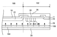
【解決手段】第一導電型のエミッタ領域と、該エミッタ領域と接する第二導電型のベース領域と、該ベース領域と接する第一導電型の耐圧維持領域と、該耐圧維持領域と接する第二導電型であるコレクタ領域と、該コレクタ領域と接して配置される電極であるコレクタ電極とを備える。そして、該コレクタ領域は、電界緩和領域に重なる領域と能動領域に重なる領域共に第二導電型のドーパントがあり、該電界緩和領域に重なる領域には該能動領域に重なる領域と比較して第二導電型のキャリアのキャリア密度が低い領域がある。
【選択図】図3
Description
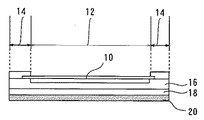
図1は本実施形態の電力用半導体装置であるIGBTチップの正面図である。そして、図2は図1のIGBTの平面図である。本実施形態のIGBTはn型で比抵抗が250〜300Ω/cmのシリコン基板16を備える。シリコン基板16の厚みは本実施形態のIGBTが耐圧特性を維持するために必要な厚み以上でなければならない。例えば、3300V用IGBTの場合シリコン基板の厚みは400μm程度である。図1でシリコン基板16の表面側には後述するMOS領域を含む能動領域12が形成される。能動領域12とはIGBTのキャリアの輸送が行われる領域である。
本実施形態はバッファ領域の活性化率の制御を行う事によりIGBTの特性を最適化できる電力用半導体装置とその製造方法に関する。本実施形態の構成については、図3で表される実施の形態1の構成との相違点のみ説明する。
28 耐圧維持領域
34 コレクタ不活性領域
38 コレクタ活性領域
92 エミッタ領域
96 ベース領域
Claims (6)
- 第一導電型のエミッタ領域と、
前記エミッタ領域と接する第二導電型のベース領域と、
前記ベース領域と接する第一導電型の耐圧維持領域と、
前記耐圧維持領域と接する第二導電型であるコレクタ領域と、
前記コレクタ領域と接して配置される電極であるコレクタ電極とを備え、
前記コレクタ領域は、電界緩和領域に重なる領域と能動領域に重なる領域共に第二導電型のドーパントがあり、前記電界緩和領域に重なる領域には前記能動領域に重なる領域と比較して第二導電型のキャリアのキャリア密度が低い領域がある事を特徴とする電力用半導体装置。 - 前記耐圧維持領域と前記コレクタ領域の中間には、第一導電型であり、かつ前記耐圧維持領域よりは第一導電型のキャリアのキャリア密度が高いバッファ領域が形成されていることを特徴とする請求項1に記載の電力用半導体装置。
- 第一導電型のエミッタ領域と、
前記エミッタ領域と接する第二導電型のベース領域と、
前記ベース領域と接する第一導電型の耐圧維持領域と、
前記耐圧維持領域と接する第二導電型であるコレクタ領域と、
前記耐圧維持領域と前記コレクタ領域の中間に配置される、第一導電型であり、かつ前記耐圧維持領域よりは第一導電型のキャリアのキャリア密度が高いバッファ領域と、
前記コレクタ領域と接して配置される電極であるコレクタ電極とを備え、
前記バッファ領域の電界緩和領域に重なる領域には、能動領域に重なる領域と比較して第一導電型のキャリアのキャリア密度が高い領域がある事を特徴とする電力用半導体装置。 - 前記耐圧維持領域の前記電界緩和領域に重なる領域に
第二導電型の領域であるガードリングと、
前記ガードリングの形成される領域よりも前記能動領域から離れた領域に前記耐圧維持領域よりも第一導電型のキャリアのキャリア密度が高い第一導電型の領域であるチャネルストッパー領域とを備える事を特徴とする請求項1〜3のいずれかに記載の電力用半導体装置。 - 裏面研削機でウェーハ裏面を研削する裏面研削工程と、
前記ウェーハ裏面からイオン注入を行いコレクタ領域を形成するコレクタ形成工程と、
レーザアニール処理により、前記コレクタ形成工程で注入されたイオンを活性化するコレクタ活性化工程と、
前記ウェーハ裏面に電極を形成する電極形成工程と、
前記電極形成工程で形成された電極を加熱する電極加熱工程とを備え、
前記コレクタ活性化工程には、前記コレクタ領域の電界緩和領域に重なる領域は能動領域に重なる領域より低いレーザパワーで前記レーザアニール処理が行われる領域があることを特徴とする電力用半導体装置の製造方法。 - イオン注入により、前記コレクタ領域より前記ウェーハ裏面から深い場所に前記コレクタ領域と導電型の異なるバッファ領域を形成するバッファ形成工程と、
レーザアニール処理により、前記バッファ形成工程で注入されたイオンを活性化するバッファ活性化工程とを備え、
前記バッファ活性化工程では、前記バッファ領域の前記電界緩和領域に重なる領域と前記能動領域に重なる領域とが同等のレーザパワーで、又は前記電界緩和領域に重なる領域は前記能動領域に重なる領域より強いレーザパワーで前記レーザアニール処理が行われる事を特徴とする請求項5に記載の電力用半導体装置の製造方法。
Priority Applications (5)
| Application Number | Priority Date | Filing Date | Title |
|---|---|---|---|
| JP2007180931A JP5286706B2 (ja) | 2007-07-10 | 2007-07-10 | 電力用半導体装置とその製造方法 |
| US11/937,725 US8742474B2 (en) | 2007-07-10 | 2007-11-09 | Power semiconductor device having an active region and an electric field reduction region |
| KR1020080008409A KR100962524B1 (ko) | 2007-07-10 | 2008-01-28 | 전력용 반도체장치와 그 제조 방법 |
| DE102008008152.3A DE102008008152B4 (de) | 2007-07-10 | 2008-02-08 | Leistungshalbleitervorrichtung |
| CN200810074210XA CN101345255B (zh) | 2007-07-10 | 2008-02-13 | 功率用半导体装置及其制造方法 |
Applications Claiming Priority (1)
| Application Number | Priority Date | Filing Date | Title |
|---|---|---|---|
| JP2007180931A JP5286706B2 (ja) | 2007-07-10 | 2007-07-10 | 電力用半導体装置とその製造方法 |
Publications (2)
| Publication Number | Publication Date |
|---|---|
| JP2009021285A true JP2009021285A (ja) | 2009-01-29 |
| JP5286706B2 JP5286706B2 (ja) | 2013-09-11 |
Family
ID=40121628
Family Applications (1)
| Application Number | Title | Priority Date | Filing Date |
|---|---|---|---|
| JP2007180931A Active JP5286706B2 (ja) | 2007-07-10 | 2007-07-10 | 電力用半導体装置とその製造方法 |
Country Status (5)
| Country | Link |
|---|---|
| US (1) | US8742474B2 (ja) |
| JP (1) | JP5286706B2 (ja) |
| KR (1) | KR100962524B1 (ja) |
| CN (1) | CN101345255B (ja) |
| DE (1) | DE102008008152B4 (ja) |
Families Citing this family (18)
| Publication number | Priority date | Publication date | Assignee | Title |
|---|---|---|---|---|
| DE102007062305B3 (de) * | 2007-12-21 | 2009-05-28 | Semikron Elektronik Gmbh & Co. Kg | Leistungshalbleiterbauelement mit grabenförmiger Feldringstruktur und Herstellungsverfahren hierzu |
| CN102473723B (zh) * | 2009-07-15 | 2014-12-03 | 三菱电机株式会社 | 功率用半导体装置及其制造方法 |
| JP2011204711A (ja) * | 2010-03-24 | 2011-10-13 | Toshiba Corp | 半導体装置およびその製造方法 |
| CN102208436B (zh) * | 2010-03-31 | 2013-10-02 | 比亚迪股份有限公司 | 功率半导体器件的终端结构及功率半导体器件 |
| JP5606240B2 (ja) * | 2010-09-22 | 2014-10-15 | 三菱電機株式会社 | 半導体装置 |
| US9041051B2 (en) * | 2011-07-05 | 2015-05-26 | Mitsubishi Electric Corporation | Semiconductor device |
| JP5713116B2 (ja) * | 2011-11-22 | 2015-05-07 | トヨタ自動車株式会社 | 半導体装置 |
| JP5811829B2 (ja) * | 2011-12-22 | 2015-11-11 | 住友電気工業株式会社 | 半導体装置の製造方法 |
| CN102543728A (zh) * | 2012-01-05 | 2012-07-04 | 深圳市鹏微科技有限公司 | 功率三极管芯片薄片制造方法 |
| CN103681816A (zh) * | 2012-09-09 | 2014-03-26 | 苏州英能电子科技有限公司 | 一种具有浮置环结构的双极型晶体管 |
| CN103681809B (zh) * | 2012-09-09 | 2016-08-17 | 苏州英能电子科技有限公司 | 具有复合结构的横向双极型晶体管 |
| KR102045730B1 (ko) * | 2012-12-28 | 2019-12-03 | 엘지디스플레이 주식회사 | 인버터와 이를 이용한 구동회로 및 표시장치 |
| CN104979283B (zh) * | 2014-04-03 | 2020-06-19 | 中国科学院微电子研究所 | Ti-igbt的制作方法 |
| JP6624101B2 (ja) | 2017-02-03 | 2019-12-25 | 株式会社デンソー | 半導体装置 |
| JP6958732B2 (ja) * | 2018-05-10 | 2021-11-02 | 富士電機株式会社 | 半導体装置の製造方法 |
| CN109671771B (zh) * | 2018-11-19 | 2022-04-01 | 全球能源互联网研究院有限公司 | Igbt芯片的背面结构、igbt芯片结构及制备方法 |
| CN109860283B (zh) * | 2019-01-16 | 2024-09-20 | 全球能源互联网研究院有限公司 | 一种igbt、igbt背面的制作方法和装置 |
| CN111682062A (zh) * | 2020-06-24 | 2020-09-18 | 全球能源互联网研究院有限公司 | 一种igbt器件的背面结构及其制备方法、igbt器件 |
Citations (9)
| Publication number | Priority date | Publication date | Assignee | Title |
|---|---|---|---|---|
| JPH0430476A (ja) * | 1990-05-25 | 1992-02-03 | Fuji Electric Co Ltd | 絶縁ゲートバイポーラトランジスタ |
| JPH0661495A (ja) * | 1992-08-07 | 1994-03-04 | Hitachi Ltd | 半導体装置及びその製法 |
| JPH09199713A (ja) * | 1996-01-16 | 1997-07-31 | Mitsubishi Electric Corp | 半導体装置 |
| JPH10173174A (ja) * | 1996-12-06 | 1998-06-26 | Toshiba Corp | 半導体装置とその製造方法 |
| JP2001160559A (ja) * | 1999-12-01 | 2001-06-12 | Fuji Electric Co Ltd | 半導体装置の製造方法 |
| JP2002359373A (ja) * | 2001-03-29 | 2002-12-13 | Toshiba Corp | 半導体装置及びその製造方法 |
| JP2003318400A (ja) * | 2002-04-23 | 2003-11-07 | Toyota Central Res & Dev Lab Inc | 半導体装置とその製造方法 |
| JP2005136092A (ja) * | 2003-10-29 | 2005-05-26 | Honda Motor Co Ltd | 半導体装置とその製造方法 |
| JP2007134714A (ja) * | 2005-11-09 | 2007-05-31 | Infineon Technologies Ag | 高い強度をもつパワーigbt |
Family Cites Families (12)
| Publication number | Priority date | Publication date | Assignee | Title |
|---|---|---|---|---|
| JP3437863B2 (ja) * | 1993-01-18 | 2003-08-18 | 株式会社半導体エネルギー研究所 | Mis型半導体装置の作製方法 |
| DE4313170A1 (de) * | 1993-04-22 | 1994-10-27 | Abb Management Ag | Leistungshalbleiterbauelement |
| JP3325752B2 (ja) | 1995-12-11 | 2002-09-17 | 三菱電機株式会社 | 半導体装置およびその製造方法 |
| JP4566470B2 (ja) * | 2001-07-17 | 2010-10-20 | 三菱電機株式会社 | 絶縁ゲート型バイポーラトランジスタ |
| KR100854078B1 (ko) * | 2001-09-12 | 2008-08-25 | 페어차일드코리아반도체 주식회사 | 모스 게이트형 전력용 반도체소자 및 그 제조방법 |
| JP4097416B2 (ja) | 2001-10-26 | 2008-06-11 | 新電元工業株式会社 | 絶縁ゲート型バイポーラトランジスタ及びその製造方法 |
| JP2003347547A (ja) | 2002-05-27 | 2003-12-05 | Mitsubishi Electric Corp | 電力用半導体装置及びその製造方法 |
| DE10330571B8 (de) | 2003-07-07 | 2007-03-08 | Infineon Technologies Ag | Vertikale Leistungshalbleiterbauelemente mit Injektionsdämpfungsmittel im Rand bereich und Herstellungsverfahren dafür |
| JP4264316B2 (ja) * | 2003-09-01 | 2009-05-13 | 株式会社豊田中央研究所 | 半導体装置とその製造方法 |
| JP4231387B2 (ja) | 2003-11-05 | 2009-02-25 | 本田技研工業株式会社 | 半導体装置とその製造方法 |
| JP2005333055A (ja) | 2004-05-21 | 2005-12-02 | Toyota Central Res & Dev Lab Inc | 半導体装置 |
| JP4770140B2 (ja) | 2004-08-17 | 2011-09-14 | 富士電機株式会社 | 半導体素子の製造方法 |
-
2007
- 2007-07-10 JP JP2007180931A patent/JP5286706B2/ja active Active
- 2007-11-09 US US11/937,725 patent/US8742474B2/en active Active
-
2008
- 2008-01-28 KR KR1020080008409A patent/KR100962524B1/ko active Active
- 2008-02-08 DE DE102008008152.3A patent/DE102008008152B4/de active Active
- 2008-02-13 CN CN200810074210XA patent/CN101345255B/zh active Active
Patent Citations (9)
| Publication number | Priority date | Publication date | Assignee | Title |
|---|---|---|---|---|
| JPH0430476A (ja) * | 1990-05-25 | 1992-02-03 | Fuji Electric Co Ltd | 絶縁ゲートバイポーラトランジスタ |
| JPH0661495A (ja) * | 1992-08-07 | 1994-03-04 | Hitachi Ltd | 半導体装置及びその製法 |
| JPH09199713A (ja) * | 1996-01-16 | 1997-07-31 | Mitsubishi Electric Corp | 半導体装置 |
| JPH10173174A (ja) * | 1996-12-06 | 1998-06-26 | Toshiba Corp | 半導体装置とその製造方法 |
| JP2001160559A (ja) * | 1999-12-01 | 2001-06-12 | Fuji Electric Co Ltd | 半導体装置の製造方法 |
| JP2002359373A (ja) * | 2001-03-29 | 2002-12-13 | Toshiba Corp | 半導体装置及びその製造方法 |
| JP2003318400A (ja) * | 2002-04-23 | 2003-11-07 | Toyota Central Res & Dev Lab Inc | 半導体装置とその製造方法 |
| JP2005136092A (ja) * | 2003-10-29 | 2005-05-26 | Honda Motor Co Ltd | 半導体装置とその製造方法 |
| JP2007134714A (ja) * | 2005-11-09 | 2007-05-31 | Infineon Technologies Ag | 高い強度をもつパワーigbt |
Also Published As
| Publication number | Publication date |
|---|---|
| KR100962524B1 (ko) | 2010-06-14 |
| US8742474B2 (en) | 2014-06-03 |
| DE102008008152A1 (de) | 2009-01-15 |
| JP5286706B2 (ja) | 2013-09-11 |
| CN101345255B (zh) | 2010-08-11 |
| DE102008008152B4 (de) | 2014-11-20 |
| KR20090005947A (ko) | 2009-01-14 |
| US20090014753A1 (en) | 2009-01-15 |
| CN101345255A (zh) | 2009-01-14 |
Similar Documents
| Publication | Publication Date | Title |
|---|---|---|
| JP5286706B2 (ja) | 電力用半導体装置とその製造方法 | |
| JP5605073B2 (ja) | 半導体装置 | |
| JP6078961B2 (ja) | 半導体装置の製造方法 | |
| JP6676988B2 (ja) | 半導体装置 | |
| US9941395B2 (en) | Insulated gate semiconductor device and method for manufacturing the same | |
| CN109585529B (zh) | 半导体装置及其制造方法 | |
| CN104303285B (zh) | 半导体装置以及半导体装置的制造方法 | |
| CN110649090A (zh) | 半导体装置、半导体装置的制造方法 | |
| JP6784148B2 (ja) | 半導体装置、絶縁ゲート型バイポーラトランジスタ、絶縁ゲート型バイポーラトランジスタの製造方法 | |
| US9543405B2 (en) | Method of manufacturing a reduced free-charge carrier lifetime semiconductor structure | |
| JP2016063072A (ja) | 半導体装置の製造方法 | |
| JP2012069634A (ja) | 半導体装置 | |
| JP7410478B2 (ja) | 炭化珪素半導体装置および炭化珪素半導体装置の製造方法 | |
| JP2015023141A (ja) | 半導体装置 | |
| CN110419111B (zh) | 自对准且稳健的绝缘栅双极晶体管器件 | |
| JP4910894B2 (ja) | 半導体装置の製造方法および半導体装置 | |
| CN103872108A (zh) | 一种igbt结构及其制备方法 | |
| CN109564939B (zh) | 半导体装置 | |
| US20110006339A1 (en) | Semiconductor device and method of manufacturing the same | |
| JP6020317B2 (ja) | 半導体素子 | |
| CN216250740U (zh) | 功率半导体器件 | |
| EP2602826A1 (en) | Insulated gate power semiconductor device and method for manufacturing such a device | |
| JP2008147318A (ja) | 高耐圧半導体装置及びその製造方法 | |
| US20250072023A1 (en) | Semiconductor device | |
| JP7524589B2 (ja) | 半導体装置 |
Legal Events
| Date | Code | Title | Description |
|---|---|---|---|
| A621 | Written request for application examination |
Free format text: JAPANESE INTERMEDIATE CODE: A621 Effective date: 20091120 |
|
| A131 | Notification of reasons for refusal |
Free format text: JAPANESE INTERMEDIATE CODE: A131 Effective date: 20120828 |
|
| A977 | Report on retrieval |
Free format text: JAPANESE INTERMEDIATE CODE: A971007 Effective date: 20120830 |
|
| A521 | Request for written amendment filed |
Free format text: JAPANESE INTERMEDIATE CODE: A523 Effective date: 20121011 |
|
| A131 | Notification of reasons for refusal |
Free format text: JAPANESE INTERMEDIATE CODE: A131 Effective date: 20130226 |
|
| A521 | Request for written amendment filed |
Free format text: JAPANESE INTERMEDIATE CODE: A523 Effective date: 20130410 |
|
| TRDD | Decision of grant or rejection written | ||
| A01 | Written decision to grant a patent or to grant a registration (utility model) |
Free format text: JAPANESE INTERMEDIATE CODE: A01 Effective date: 20130507 |
|
| A61 | First payment of annual fees (during grant procedure) |
Free format text: JAPANESE INTERMEDIATE CODE: A61 Effective date: 20130520 |
|
| R150 | Certificate of patent or registration of utility model |
Ref document number: 5286706 Country of ref document: JP Free format text: JAPANESE INTERMEDIATE CODE: R150 |
|
| R250 | Receipt of annual fees |
Free format text: JAPANESE INTERMEDIATE CODE: R250 |
|
| R250 | Receipt of annual fees |
Free format text: JAPANESE INTERMEDIATE CODE: R250 |
|
| R250 | Receipt of annual fees |
Free format text: JAPANESE INTERMEDIATE CODE: R250 |
|
| R250 | Receipt of annual fees |
Free format text: JAPANESE INTERMEDIATE CODE: R250 |
|
| R250 | Receipt of annual fees |
Free format text: JAPANESE INTERMEDIATE CODE: R250 |
|
| R250 | Receipt of annual fees |
Free format text: JAPANESE INTERMEDIATE CODE: R250 |
|
| R250 | Receipt of annual fees |
Free format text: JAPANESE INTERMEDIATE CODE: R250 |
|
| R250 | Receipt of annual fees |
Free format text: JAPANESE INTERMEDIATE CODE: R250 |
|
| R250 | Receipt of annual fees |
Free format text: JAPANESE INTERMEDIATE CODE: R250 |
|
| R250 | Receipt of annual fees |
Free format text: JAPANESE INTERMEDIATE CODE: R250 |