JP2009043826A - 撮像装置及び放射線撮像システム - Google Patents
撮像装置及び放射線撮像システム Download PDFInfo
- Publication number
- JP2009043826A JP2009043826A JP2007205472A JP2007205472A JP2009043826A JP 2009043826 A JP2009043826 A JP 2009043826A JP 2007205472 A JP2007205472 A JP 2007205472A JP 2007205472 A JP2007205472 A JP 2007205472A JP 2009043826 A JP2009043826 A JP 2009043826A
- Authority
- JP
- Japan
- Prior art keywords
- conversion element
- signal
- line
- lines
- protective layer
- Prior art date
- Legal status (The legal status is an assumption and is not a legal conclusion. Google has not performed a legal analysis and makes no representation as to the accuracy of the status listed.)
- Granted
Links
Images


Classifications
-
- H—ELECTRICITY
- H10—SEMICONDUCTOR DEVICES; ELECTRIC SOLID-STATE DEVICES NOT OTHERWISE PROVIDED FOR
- H10F—INORGANIC SEMICONDUCTOR DEVICES SENSITIVE TO INFRARED RADIATION, LIGHT, ELECTROMAGNETIC RADIATION OF SHORTER WAVELENGTH OR CORPUSCULAR RADIATION
- H10F39/00—Integrated devices, or assemblies of multiple devices, comprising at least one element covered by group H10F30/00, e.g. radiation detectors comprising photodiode arrays
- H10F39/10—Integrated devices
- H10F39/12—Image sensors
- H10F39/18—Complementary metal-oxide-semiconductor [CMOS] image sensors; Photodiode array image sensors
- H10F39/189—X-ray, gamma-ray or corpuscular radiation imagers
- H10F39/1898—Indirect radiation image sensors, e.g. using luminescent members
Landscapes
- Measurement Of Radiation (AREA)
- Solid State Image Pick-Up Elements (AREA)
- Light Receiving Elements (AREA)
Abstract
【解決手段】変換素子10、変換素子10に接続されたTFT14とを有する複数の画素、複数の画素上に配置された保護層27、変換素子に電気的に接続された複数のバイアス線11、TFT14に電気的に接続された複数の信号線12を具備する。複数のバイアス線11と複数の信号線12は保護層27の領域内で所定間隔で交互に配置する。複数のバイアス線11は保護層27の領域外で接続配線17によって共通化し、接続配線17は複数の信号線12と交差して配置する。
【選択図】図2
Description
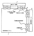
図1は発明に係る撮像装置としてのX線撮像装置の実施形態1を示す平面図、図2は図1中のA部分を拡大して示す平面図である。また、図3は図2のB−B’線における1画素の断面図、図4は図2のC−C’線における断面図、図5は図2のD−D’線における断面図、図6は図2のE−E’線における断面図である。各図面において、X線などの放射線を可視光に変換するシンチレータ層は、図示していない。
(1)画素領域に対して一方の端部のみに配置する。
(2)画素領域に対して両端部に配置する。
(3)各読み出し回路接続部6の両端部に配置する。
これらの配置例において、いずれの配置も画像ムラを低減することができる。
次に、本発明の撮像装置の実施形態2について説明する。本実施形態の撮像装置の基本構成及び動作原理は実施形態1と同様であるため詳細な説明は省略する。図7は図1のA部分を拡大して示す平面図、図8は図7のF−F’線における断面図、図9は図7のG−G’における断面図である。図7〜図9では図2〜図6と同一部分には同一符号を付している。
図10は本発明に係る撮像装置としての放射線撮像装置を用いた放射線撮像システムの一実施形態としてのX線診断システムを示す。
2 駆動回路
4 ゲート駆動回路
5 読み出し回路
7 読み出し装置
10 MIS型光電変換素子
11 Vs配線
12 Sig線
13 Vg線
14 TFT
15 引き出し配線
16 外部回路接続電極
17 Vs接続配線
19 絶縁基板
20 第1の電極層
21 第1の絶縁層
22 半導体層
23 不純物半導体層
24 第2の電極層
25 第3の電極層
26 第2の絶縁層
27 保護層
28 接着層
29 シンチレータ層
Claims (4)
- 入射する放射線を電気信号に変換するセンサ基板を有する撮像装置において、
前記センサ基板は、
変換素子と、前記変換素子に接続されたスイッチ素子とを有する複数の画素と、
前記複数の画素上に配置された保護層と、
前記変換素子に電気的に接続された複数のバイアス線と、
前記スイッチ素子に電気的に接続された複数の信号線とを有し、
前記複数のバイアス線の各々と前記複数の信号線の各々は前記保護層の領域内で所定間隔で交互に配置され、
前記複数のバイアス線は前記保護層の領域外で接続配線によって共通化され、且つ、前記接続配線は前記複数の信号線と交差して配置されていることを特徴とする撮像装置。 - 前記複数のバイアス線を外部回路接続電極に引き出す引き出し配線と、前記複数の信号線を外部回路接続電極に引き出す引き出し配線とは、異なる金属層で形成されていることを特徴とする請求項1に記載の撮像装置。
- 前記変換素子が光電変換素子であり、前記光電変換素子上に配置されたシンチレータ層を有することを特徴とする請求項1に記載の撮像装置。
- 請求項1〜3のいずれか1項に記載の撮像装置と、
前記撮像装置からの信号を処理する信号処理手段と、
前記信号処理手段からの信号を記録するための記録手段と、
前記信号処理手段からの信号を表示するための表示手段と、
前記信号処理手段からの信号を伝送するための伝送処理手段と、
前記放射線を発生させるための放射線源と、を具備することを特徴とする放射線撮像システム。
Priority Applications (2)
| Application Number | Priority Date | Filing Date | Title |
|---|---|---|---|
| JP2007205472A JP5235350B2 (ja) | 2007-08-07 | 2007-08-07 | 撮像装置及び放射線撮像システム |
| US12/185,445 US7932946B2 (en) | 2007-08-07 | 2008-08-04 | Imaging apparatus and radiation imaging system |
Applications Claiming Priority (1)
| Application Number | Priority Date | Filing Date | Title |
|---|---|---|---|
| JP2007205472A JP5235350B2 (ja) | 2007-08-07 | 2007-08-07 | 撮像装置及び放射線撮像システム |
Publications (3)
| Publication Number | Publication Date |
|---|---|
| JP2009043826A true JP2009043826A (ja) | 2009-02-26 |
| JP2009043826A5 JP2009043826A5 (ja) | 2010-08-19 |
| JP5235350B2 JP5235350B2 (ja) | 2013-07-10 |
Family
ID=40346102
Family Applications (1)
| Application Number | Title | Priority Date | Filing Date |
|---|---|---|---|
| JP2007205472A Expired - Fee Related JP5235350B2 (ja) | 2007-08-07 | 2007-08-07 | 撮像装置及び放射線撮像システム |
Country Status (2)
| Country | Link |
|---|---|
| US (1) | US7932946B2 (ja) |
| JP (1) | JP5235350B2 (ja) |
Cited By (2)
| Publication number | Priority date | Publication date | Assignee | Title |
|---|---|---|---|---|
| WO2016104339A1 (ja) * | 2014-12-25 | 2016-06-30 | シャープ株式会社 | フォトセンサ基板、及びその製造方法 |
| WO2016195000A1 (ja) * | 2015-06-04 | 2016-12-08 | シャープ株式会社 | フォトセンサ基板 |
Families Citing this family (22)
| Publication number | Priority date | Publication date | Assignee | Title |
|---|---|---|---|---|
| JP5196739B2 (ja) | 2006-06-09 | 2013-05-15 | キヤノン株式会社 | 放射線撮像装置及び放射線撮像システム |
| JP5489542B2 (ja) * | 2008-07-01 | 2014-05-14 | キヤノン株式会社 | 放射線検出装置及び放射線撮像システム |
| JP5439837B2 (ja) | 2009-02-10 | 2014-03-12 | ソニー株式会社 | 表示装置 |
| JP5954983B2 (ja) | 2011-12-21 | 2016-07-20 | キヤノン株式会社 | 撮像装置及び放射線撮像システム、並びに撮像装置の製造方法 |
| JP6057511B2 (ja) | 2011-12-21 | 2017-01-11 | キヤノン株式会社 | 撮像装置及び放射線撮像システム |
| JP6480670B2 (ja) | 2014-05-01 | 2019-03-13 | キヤノン株式会社 | 放射線撮像装置および放射線撮像システム |
| JP6585910B2 (ja) | 2014-05-01 | 2019-10-02 | キヤノン株式会社 | 放射線撮像装置および放射線撮像システム |
| JP6570315B2 (ja) | 2015-05-22 | 2019-09-04 | キヤノン株式会社 | 放射線撮像装置及び放射線撮像システム |
| JP6929104B2 (ja) | 2017-04-05 | 2021-09-01 | キヤノン株式会社 | 放射線撮像装置、放射線撮像システム、放射線撮像装置の制御方法及びプログラム |
| JP6928746B2 (ja) * | 2017-04-10 | 2021-09-01 | ブリルニクス シンガポール プライベート リミテッド | 固体撮像装置、固体撮像装置の製造方法、および電子機器 |
| JP6990986B2 (ja) | 2017-04-27 | 2022-01-12 | キヤノン株式会社 | 放射線撮像装置、放射線撮像システム、放射線撮像装置の制御方法及びプログラム |
| JP6853729B2 (ja) | 2017-05-08 | 2021-03-31 | キヤノン株式会社 | 放射線撮像装置、放射線撮像システム、放射線撮像装置の制御方法及びプログラム |
| JP6788547B2 (ja) * | 2017-05-09 | 2020-11-25 | キヤノン株式会社 | 放射線撮像装置、その制御方法、制御装置、及び、放射線撮像システム |
| JP6877289B2 (ja) | 2017-07-31 | 2021-05-26 | キヤノン株式会社 | 放射線検出装置、放射線検出システム、及び放射線出装置の製造方法 |
| JP7045834B2 (ja) | 2017-11-10 | 2022-04-01 | キヤノン株式会社 | 放射線撮像システム |
| JP7079113B2 (ja) | 2018-02-21 | 2022-06-01 | キヤノン株式会社 | 放射線撮像装置及び放射線撮像システム |
| JP7198003B2 (ja) | 2018-06-22 | 2022-12-28 | キヤノン株式会社 | 放射線撮像装置、放射線撮像システム、放射線撮像装置の制御方法およびプログラム |
| JP6659182B2 (ja) | 2018-07-23 | 2020-03-04 | キヤノン株式会社 | 放射線撮像装置、その製造方法及び放射線撮像システム |
| EP3661190B1 (en) | 2018-11-27 | 2024-05-22 | Canon Kabushiki Kaisha | Radiation imaging apparatus and radiation imaging system |
| JP7397635B2 (ja) | 2019-11-22 | 2023-12-13 | キヤノン株式会社 | 放射線検出装置、放射線検出システム、制御方法及びプログラム |
| JP7344769B2 (ja) | 2019-11-22 | 2023-09-14 | キヤノン株式会社 | 放射線検出装置及び出力方法 |
| JP2023117956A (ja) | 2022-02-14 | 2023-08-24 | キヤノン株式会社 | センサ基板、放射線撮像装置、放射線撮像システム、および、センサ基板の製造方法 |
Citations (4)
| Publication number | Priority date | Publication date | Assignee | Title |
|---|---|---|---|---|
| JP2003270351A (ja) * | 2002-03-12 | 2003-09-25 | Canon Inc | 放射線撮像装置 |
| JP2004184273A (ja) * | 2002-12-04 | 2004-07-02 | Casio Comput Co Ltd | デバイス検査方法 |
| JP2006189377A (ja) * | 2005-01-07 | 2006-07-20 | Canon Inc | シンチレータパネル、放射線検出装置、及び放射線検出システム |
| JP2007049123A (ja) * | 2005-07-11 | 2007-02-22 | Canon Inc | 変換装置、放射線検出装置、及び放射線検出システム |
Family Cites Families (5)
| Publication number | Priority date | Publication date | Assignee | Title |
|---|---|---|---|---|
| JP2002050754A (ja) * | 2000-05-08 | 2002-02-15 | Canon Inc | 半導体装置とその製造方法、放射線検出装置とそれを用いた放射線検出システム |
| JP2004325261A (ja) * | 2003-04-24 | 2004-11-18 | Canon Inc | 放射線画像撮像装置 |
| JP4845352B2 (ja) * | 2004-06-15 | 2011-12-28 | キヤノン株式会社 | 放射線撮像装置、その製造方法及び放射線撮像システム |
| JP4908947B2 (ja) * | 2005-07-11 | 2012-04-04 | キヤノン株式会社 | 変換装置、放射線検出装置、及び放射線検出システム |
| JP5173234B2 (ja) * | 2006-05-24 | 2013-04-03 | キヤノン株式会社 | 放射線撮像装置及び放射線撮像システム |
-
2007
- 2007-08-07 JP JP2007205472A patent/JP5235350B2/ja not_active Expired - Fee Related
-
2008
- 2008-08-04 US US12/185,445 patent/US7932946B2/en not_active Expired - Fee Related
Patent Citations (4)
| Publication number | Priority date | Publication date | Assignee | Title |
|---|---|---|---|---|
| JP2003270351A (ja) * | 2002-03-12 | 2003-09-25 | Canon Inc | 放射線撮像装置 |
| JP2004184273A (ja) * | 2002-12-04 | 2004-07-02 | Casio Comput Co Ltd | デバイス検査方法 |
| JP2006189377A (ja) * | 2005-01-07 | 2006-07-20 | Canon Inc | シンチレータパネル、放射線検出装置、及び放射線検出システム |
| JP2007049123A (ja) * | 2005-07-11 | 2007-02-22 | Canon Inc | 変換装置、放射線検出装置、及び放射線検出システム |
Cited By (3)
| Publication number | Priority date | Publication date | Assignee | Title |
|---|---|---|---|---|
| WO2016104339A1 (ja) * | 2014-12-25 | 2016-06-30 | シャープ株式会社 | フォトセンサ基板、及びその製造方法 |
| WO2016195000A1 (ja) * | 2015-06-04 | 2016-12-08 | シャープ株式会社 | フォトセンサ基板 |
| US10276611B2 (en) | 2015-06-04 | 2019-04-30 | Sharp Kabushiki Kaisha | Photosensor substrate |
Also Published As
| Publication number | Publication date |
|---|---|
| US20090040348A1 (en) | 2009-02-12 |
| US7932946B2 (en) | 2011-04-26 |
| JP5235350B2 (ja) | 2013-07-10 |
Similar Documents
| Publication | Publication Date | Title |
|---|---|---|
| JP5235350B2 (ja) | 撮像装置及び放射線撮像システム | |
| JP6442163B2 (ja) | 放射線撮像装置および放射線撮像システム | |
| JP6480670B2 (ja) | 放射線撮像装置および放射線撮像システム | |
| JP5159065B2 (ja) | 放射線検出装置、放射線撮像装置および放射線撮像システム | |
| US8067743B2 (en) | Imaging apparatus and radiation imaging apparatus | |
| JP4750512B2 (ja) | 放射線撮像装置、その制御方法及び放射線撮像システム | |
| JP4845352B2 (ja) | 放射線撮像装置、その製造方法及び放射線撮像システム | |
| JP5043373B2 (ja) | 変換装置、放射線検出装置、及び放射線検出システム | |
| JP5328169B2 (ja) | 撮像装置及び放射線撮像システム | |
| JP5700973B2 (ja) | 検出装置及び放射線検出システム | |
| JP2007049124A (ja) | 変換装置、放射線検出装置、及び放射線検出システム | |
| JP5400507B2 (ja) | 撮像装置及び放射線撮像システム | |
| JP4067055B2 (ja) | 撮像装置及びその製造方法、放射線撮像装置、放射線撮像システム | |
| CN114423350A (zh) | 放射线成像装置和放射线成像系统 | |
| JP4908947B2 (ja) | 変換装置、放射線検出装置、及び放射線検出システム | |
| JP2012079860A (ja) | 検出装置及び放射線検出システム | |
| JP2004251892A (ja) | 放射線撮像装置及び放射線撮像システム | |
| JP2012079820A (ja) | 検出装置及び放射線検出システム | |
| JP6470508B2 (ja) | 放射線撮像装置および放射線撮像システム | |
| JP2008141705A (ja) | 放射線撮像装置及び放射線撮像システム | |
| JP5677353B2 (ja) | 放射線検出装置および放射線撮像システム | |
| JP2016201665A (ja) | 放射線撮像装置および放射線撮像システム | |
| JP2006005150A (ja) | 撮像装置及び放射線撮像装置、放射線撮像システム | |
| JP2018021828A (ja) | 放射線撮像装置及び放射線撮像システム | |
| JP2007184407A (ja) | 電磁波検出装置及び放射線撮像システム |
Legal Events
| Date | Code | Title | Description |
|---|---|---|---|
| RD03 | Notification of appointment of power of attorney |
Free format text: JAPANESE INTERMEDIATE CODE: A7423 Effective date: 20090326 |
|
| RD05 | Notification of revocation of power of attorney |
Free format text: JAPANESE INTERMEDIATE CODE: A7425 Effective date: 20090427 |
|
| A521 | Request for written amendment filed |
Free format text: JAPANESE INTERMEDIATE CODE: A523 Effective date: 20100630 |
|
| A621 | Written request for application examination |
Free format text: JAPANESE INTERMEDIATE CODE: A621 Effective date: 20100630 |
|
| A977 | Report on retrieval |
Free format text: JAPANESE INTERMEDIATE CODE: A971007 Effective date: 20120912 |
|
| A131 | Notification of reasons for refusal |
Free format text: JAPANESE INTERMEDIATE CODE: A131 Effective date: 20120921 |
|
| A521 | Request for written amendment filed |
Free format text: JAPANESE INTERMEDIATE CODE: A523 Effective date: 20121114 |
|
| A131 | Notification of reasons for refusal |
Free format text: JAPANESE INTERMEDIATE CODE: A131 Effective date: 20121207 |
|
| A521 | Request for written amendment filed |
Free format text: JAPANESE INTERMEDIATE CODE: A523 Effective date: 20130205 |
|
| TRDD | Decision of grant or rejection written | ||
| A01 | Written decision to grant a patent or to grant a registration (utility model) |
Free format text: JAPANESE INTERMEDIATE CODE: A01 Effective date: 20130225 |
|
| A61 | First payment of annual fees (during grant procedure) |
Free format text: JAPANESE INTERMEDIATE CODE: A61 Effective date: 20130326 |
|
| R151 | Written notification of patent or utility model registration |
Ref document number: 5235350 Country of ref document: JP Free format text: JAPANESE INTERMEDIATE CODE: R151 |
|
| FPAY | Renewal fee payment (event date is renewal date of database) |
Free format text: PAYMENT UNTIL: 20160405 Year of fee payment: 3 |
|
| LAPS | Cancellation because of no payment of annual fees |