JP2009081702A - アンテナ装置及びその特性調整方法 - Google Patents
アンテナ装置及びその特性調整方法 Download PDFInfo
- Publication number
- JP2009081702A JP2009081702A JP2007249846A JP2007249846A JP2009081702A JP 2009081702 A JP2009081702 A JP 2009081702A JP 2007249846 A JP2007249846 A JP 2007249846A JP 2007249846 A JP2007249846 A JP 2007249846A JP 2009081702 A JP2009081702 A JP 2009081702A
- Authority
- JP
- Japan
- Prior art keywords
- antenna
- pattern
- impedance
- mounting
- frequency
- Prior art date
- Legal status (The legal status is an assumption and is not a legal conclusion. Google has not performed a legal analysis and makes no representation as to the accuracy of the status listed.)
- Granted
Links
- 238000000034 method Methods 0.000 title claims description 17
- 230000001105 regulatory effect Effects 0.000 title abstract 6
- 239000000758 substrate Substances 0.000 claims abstract description 40
- 239000004020 conductor Substances 0.000 claims description 28
- 238000005259 measurement Methods 0.000 claims description 8
- 238000009966 trimming Methods 0.000 description 10
- 238000013461 design Methods 0.000 description 8
- 230000008859 change Effects 0.000 description 6
- 238000011161 development Methods 0.000 description 4
- 230000008569 process Effects 0.000 description 4
- 230000004048 modification Effects 0.000 description 3
- 238000012986 modification Methods 0.000 description 3
- 239000003989 dielectric material Substances 0.000 description 2
- 230000000694 effects Effects 0.000 description 2
- 239000000696 magnetic material Substances 0.000 description 2
- 230000005855 radiation Effects 0.000 description 2
- 238000004904 shortening Methods 0.000 description 2
- 230000008878 coupling Effects 0.000 description 1
- 238000010168 coupling process Methods 0.000 description 1
- 238000005859 coupling reaction Methods 0.000 description 1
- 230000007423 decrease Effects 0.000 description 1
- 230000035699 permeability Effects 0.000 description 1
Images






Classifications
-
- H—ELECTRICITY
- H01—ELECTRIC ELEMENTS
- H01Q—ANTENNAS, i.e. RADIO AERIALS
- H01Q1/00—Details of, or arrangements associated with, antennas
- H01Q1/36—Structural form of radiating elements, e.g. cone, spiral, umbrella; Particular materials used therewith
- H01Q1/38—Structural form of radiating elements, e.g. cone, spiral, umbrella; Particular materials used therewith formed by a conductive layer on an insulating support
-
- H—ELECTRICITY
- H01—ELECTRIC ELEMENTS
- H01Q—ANTENNAS, i.e. RADIO AERIALS
- H01Q1/00—Details of, or arrangements associated with, antennas
- H01Q1/12—Supports; Mounting means
- H01Q1/22—Supports; Mounting means by structural association with other equipment or articles
- H01Q1/24—Supports; Mounting means by structural association with other equipment or articles with receiving set
- H01Q1/241—Supports; Mounting means by structural association with other equipment or articles with receiving set used in mobile communications, e.g. GSM
- H01Q1/242—Supports; Mounting means by structural association with other equipment or articles with receiving set used in mobile communications, e.g. GSM specially adapted for hand-held use
- H01Q1/243—Supports; Mounting means by structural association with other equipment or articles with receiving set used in mobile communications, e.g. GSM specially adapted for hand-held use with built-in antennas
-
- H—ELECTRICITY
- H01—ELECTRIC ELEMENTS
- H01Q—ANTENNAS, i.e. RADIO AERIALS
- H01Q9/00—Electrically-short antennas having dimensions not more than twice the operating wavelength and consisting of conductive active radiating elements
- H01Q9/04—Resonant antennas
- H01Q9/0407—Substantially flat resonant element parallel to ground plane, e.g. patch antenna
- H01Q9/0421—Substantially flat resonant element parallel to ground plane, e.g. patch antenna with a shorting wall or a shorting pin at one end of the element
Landscapes
- Engineering & Computer Science (AREA)
- Computer Networks & Wireless Communication (AREA)
- Waveguide Aerials (AREA)
- Details Of Aerials (AREA)
Abstract
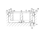
【解決手段】アンテナブロック10が実装される実装基板20には、アンテナブロック10の実装領域21の周囲に設けられたグランドパターン22と、第1乃至第3のパッド電極13〜15の位置に対応して実装領域内に設けられた第1乃至第3のランド23〜25と、第1のランド23に接続された給電ライン26と、第1のランド23とグランドパターン22とを接続するインピーダンス調整用パターン27と、第2のランド24とグランドパターン22とを接続する周波数調整用パターン28とを備えている。インピーダンス調整用パターン27の幅を変更することでアンテナのインピーダンスを粗調整でき、周波数調整用パターン28の幅を変更することで共振周波数を粗調整できる。
【選択図】図1
Description
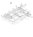
11 基体
11A アンテナブロックの上面
11B アンテナブロックの底面
11C アンテナブロックの第1の側面
11D アンテナブロックの第2の側面
11E アンテナブロックの第3の側面
11F アンテナブロックの第4の底面
12 上面導体部
13 第1のパッド電極
14 第2のパッド電極
15 第3のパッド電極
16 側面導体部
17 ギャップ
20 実装基板
21 実装領域
22 グランドパターン
23 第1のランド
23a 第1のランドのリード部分
24 第2のランド
25 第3のランド
25a 第3のランドのリード部分
26 給電ライン
27 インピーダンス調整用パターン
28 周波数調整用パターン
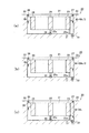
31 インピーダンス調整素子(チップリアクタ)
32 周波数調整素子(チップリアクタ)
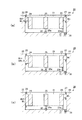
33 インピーダンス調整用スリット
34 周波数調整用スリット
34a 周波数調整用スリット
34b 周波数調整用スリット
100 アンテナ装置
200 アンテナ装置
300 アンテナ装置
W1 インピーダンス調整用パターンの幅
W2 周波数調整用パターンの幅
W3 周波数調整用パターンの幅
Claims (9)
- アンテナブロックと、前記アンテナブロックが実装された実装基板とを備え、
前記アンテナブロックは、
略直方体状の誘電体又は磁性体からなる基体と、前記基体の上面に形成された上面導体部と、前記基体の底面の長手方向の両端部にそれぞれ形成された第1及び第2のパッド電極と、前記上面導体部と前記第2のパッド電極とを接続する側面導体部とを備え、
前記実装基板は、
前記アンテナブロックの実装領域と、前記実装領域の周囲に設けられたグランドパターンと、前記第1及び第2のパッド電極の位置に対応して前記実装領域内に設けられた第1及び第2のランドと、前記第1のランドに接続された給電ラインと、前記第1のランドと前記グランドパターンとを接続するインピーダンス調整用パターンと、前記第2のランドとグランドパターンとを接続する周波数調整用パターンとを備えることを特徴とするアンテナ装置。 - 前記実装基板上に実装され、前記給電ラインと前記グランドパターンとを接続するインピーダンス調整素子をさらに備えることを特徴とする請求項1に記載のアンテナ装置。
- 前記アンテナブロックは、前記基体の底面の長手方向の中央部に設けられた第3のパッド電極をさらに備え、
前記実装基板は、前記第3のパッド電極の位置に対応して前記実装領域内に設けられた第3のランドをさらに備えることを特徴とする請求項1又は2に記載のアンテナ装置。 - 前記実装基板上に実装され、前記第3のランドと前記グランドパターンとを接続する周波数調整素子をさらに備えることを特徴とする請求項3に記載のアンテナ装置。
- 前記インピーダンス調整用パターン及び前記周波数調整用パターンの少なくとも一方を複数備えることを特徴とする請求項1に記載のアンテナ装置。
- 前記複数のインピーダンス調整用パターン又は前記複数の周波数調整用パターンの間に設けられたスペースから延設された前記グランドパターンのスリットをさらに備えることを特徴とする請求項1に記載のアンテナ装置。
- 前記スリットを複数備え、前記複数のスリットの長さがそれぞれ異なることを特徴とする請求項6に記載のアンテナ装置。
- 請求項2乃至7のいずれか一項に記載のアンテナ装置の特性調整方法であって、
所定の形状及びサイズを有する前記インピーダンス調整用パターンが形成された前記実装基板を用意し、当該実装領域に前記アンテナブロックを実装する工程と、
前記実装基板上の前記アンテナブロックのインピーダンスを測定する工程と、
前記測定結果に基づいて適切な定数を持つ前記インピーダンス調整素子を選択し、当該インピーダンス調整素子を前記実装基板上の所定の位置に実装する工程とを備えることを特徴とするアンテナ装置の特性調整方法。 - 請求項2乃至8のいずれか一項に記載のアンテナ装置の特性調整方法であって、
所定の形状及びサイズを有する前記周波数調整用パターンが形成された前記実装基板を用意し、当該実装領域に前記アンテナブロックを実装する工程と、
前記実装基板上の前記アンテナブロックの周波数を測定する工程と、
前記測定結果に基づいて適切な定数を持つ前記周波数調整素子を選択し、当該周波数調整素子を前記実装基板上の所定の位置に実装する工程とを備えることを特徴とするアンテナ装置の特性調整方法。
Priority Applications (4)
| Application Number | Priority Date | Filing Date | Title |
|---|---|---|---|
| JP2007249846A JP4941202B2 (ja) | 2007-09-26 | 2007-09-26 | アンテナ装置及びその特性調整方法 |
| US12/236,619 US7924229B2 (en) | 2007-09-26 | 2008-09-24 | Antenna apparatus and method for adjusting characteristics thereof |
| CN200810166350XA CN101399397B (zh) | 2007-09-26 | 2008-09-26 | 天线装置和调节其特性的方法 |
| EP08253147A EP2043197A1 (en) | 2007-09-26 | 2008-09-26 | Antenna apparatus and method for adjusting characteristics thereof |
Applications Claiming Priority (1)
| Application Number | Priority Date | Filing Date | Title |
|---|---|---|---|
| JP2007249846A JP4941202B2 (ja) | 2007-09-26 | 2007-09-26 | アンテナ装置及びその特性調整方法 |
Publications (2)
| Publication Number | Publication Date |
|---|---|
| JP2009081702A true JP2009081702A (ja) | 2009-04-16 |
| JP4941202B2 JP4941202B2 (ja) | 2012-05-30 |
Family
ID=40219378
Family Applications (1)
| Application Number | Title | Priority Date | Filing Date |
|---|---|---|---|
| JP2007249846A Expired - Fee Related JP4941202B2 (ja) | 2007-09-26 | 2007-09-26 | アンテナ装置及びその特性調整方法 |
Country Status (4)
| Country | Link |
|---|---|
| US (1) | US7924229B2 (ja) |
| EP (1) | EP2043197A1 (ja) |
| JP (1) | JP4941202B2 (ja) |
| CN (1) | CN101399397B (ja) |
Cited By (2)
| Publication number | Priority date | Publication date | Assignee | Title |
|---|---|---|---|---|
| JP2012151625A (ja) * | 2011-01-18 | 2012-08-09 | Mitsubishi Materials Corp | アンテナ装置 |
| JP2013239882A (ja) * | 2012-05-15 | 2013-11-28 | Mitsubishi Materials Corp | アンテナ装置 |
Families Citing this family (7)
| Publication number | Priority date | Publication date | Assignee | Title |
|---|---|---|---|---|
| JP5375719B2 (ja) * | 2010-04-01 | 2013-12-25 | Tdk株式会社 | アンテナ装置及びこれを用いた無線通信機 |
| JP5625829B2 (ja) * | 2010-11-30 | 2014-11-19 | 三菱マテリアル株式会社 | アンテナ装置 |
| CN102738579A (zh) * | 2012-07-12 | 2012-10-17 | Tdk大连电子有限公司 | 一种小型陶瓷天线 |
| CN102723596A (zh) * | 2012-07-12 | 2012-10-10 | Tdk大连电子有限公司 | 一种超薄小型陶瓷天线 |
| CN104103893A (zh) * | 2013-04-11 | 2014-10-15 | 智易科技股份有限公司 | 宽频天线装置 |
| WO2015085492A1 (zh) * | 2013-12-10 | 2015-06-18 | 华为终端有限公司 | 一种天线、天线装置、终端以及调整天线工作频段的方法 |
| KR102734771B1 (ko) * | 2019-10-01 | 2024-11-27 | 삼성전자주식회사 | 튜너블 안테나 제어 방법 및 이를 사용하는 전자 장치 |
Citations (12)
| Publication number | Priority date | Publication date | Assignee | Title |
|---|---|---|---|---|
| JPH1093331A (ja) * | 1996-09-19 | 1998-04-10 | N T T Ido Tsushinmo Kk | マイクロストリップアンテナ装置 |
| JP2002314330A (ja) * | 2001-04-10 | 2002-10-25 | Murata Mfg Co Ltd | アンテナ装置 |
| JP2002335117A (ja) * | 2001-05-08 | 2002-11-22 | Murata Mfg Co Ltd | アンテナ構造およびそれを備えた通信機 |
| JP2003078321A (ja) * | 2001-08-30 | 2003-03-14 | Murata Mfg Co Ltd | 無線通信機 |
| JP2003332831A (ja) * | 2002-05-13 | 2003-11-21 | Smkr & D Kk | アンテナ |
| JP2004096210A (ja) * | 2002-08-29 | 2004-03-25 | Hitachi Metals Ltd | 表面実装型アンテナ |
| JP2004201278A (ja) * | 2002-12-06 | 2004-07-15 | Sharp Corp | パターンアンテナ |
| JP2004356971A (ja) * | 2003-05-29 | 2004-12-16 | Sony Corp | 表面実装アンテナ及びアンテナ実装方法 |
| JP2005184547A (ja) * | 2003-12-19 | 2005-07-07 | Sony Corp | デュアルバンドアンテナ装置 |
| JP2005210665A (ja) * | 2003-12-25 | 2005-08-04 | Mitsubishi Materials Corp | アンテナ装置 |
| WO2006120763A1 (ja) * | 2005-05-13 | 2006-11-16 | Murata Manufacturing Co., Ltd. | アンテナ構造およびそれを備えた無線通信機 |
| JP2006340368A (ja) * | 2005-06-03 | 2006-12-14 | Partron Co Ltd | トリオランド構造を持つ表面実装アンテナ装置 |
Family Cites Families (8)
| Publication number | Priority date | Publication date | Assignee | Title |
|---|---|---|---|---|
| JP3435622B2 (ja) | 1997-03-07 | 2003-08-11 | 株式会社村田製作所 | 表面実装型アンテナの共振周波数調整方法、ならびにインピーダンス調整方法 |
| JP2002374115A (ja) * | 2001-06-15 | 2002-12-26 | Nec Corp | アンテナ素子、アンテナ装置、無線通信装置 |
| DE10143168A1 (de) * | 2001-09-04 | 2003-03-20 | Philips Corp Intellectual Pty | Schaltungsplatine und SMD-Antenne hierfür |
| EP1978595B1 (en) * | 2003-12-25 | 2011-03-23 | Mitsubishi Materials Corporation | Antenna device and communication apparatus |
| JP4284252B2 (ja) * | 2004-08-26 | 2009-06-24 | 京セラ株式会社 | 表面実装型アンテナおよびそれを用いたアンテナ装置ならびに無線通信装置 |
| JP2007067993A (ja) | 2005-09-01 | 2007-03-15 | Yokowo Co Ltd | アンテナ装置およびアンテナ用素子 |
| JP4775233B2 (ja) * | 2006-11-16 | 2011-09-21 | Tdk株式会社 | アンテナ装置及びそれを用いたアンテナ実装基板 |
| JP4844388B2 (ja) * | 2006-12-28 | 2011-12-28 | Tdk株式会社 | アンテナ装置 |
-
2007
- 2007-09-26 JP JP2007249846A patent/JP4941202B2/ja not_active Expired - Fee Related
-
2008
- 2008-09-24 US US12/236,619 patent/US7924229B2/en not_active Expired - Fee Related
- 2008-09-26 EP EP08253147A patent/EP2043197A1/en not_active Withdrawn
- 2008-09-26 CN CN200810166350XA patent/CN101399397B/zh not_active Expired - Fee Related
Patent Citations (12)
| Publication number | Priority date | Publication date | Assignee | Title |
|---|---|---|---|---|
| JPH1093331A (ja) * | 1996-09-19 | 1998-04-10 | N T T Ido Tsushinmo Kk | マイクロストリップアンテナ装置 |
| JP2002314330A (ja) * | 2001-04-10 | 2002-10-25 | Murata Mfg Co Ltd | アンテナ装置 |
| JP2002335117A (ja) * | 2001-05-08 | 2002-11-22 | Murata Mfg Co Ltd | アンテナ構造およびそれを備えた通信機 |
| JP2003078321A (ja) * | 2001-08-30 | 2003-03-14 | Murata Mfg Co Ltd | 無線通信機 |
| JP2003332831A (ja) * | 2002-05-13 | 2003-11-21 | Smkr & D Kk | アンテナ |
| JP2004096210A (ja) * | 2002-08-29 | 2004-03-25 | Hitachi Metals Ltd | 表面実装型アンテナ |
| JP2004201278A (ja) * | 2002-12-06 | 2004-07-15 | Sharp Corp | パターンアンテナ |
| JP2004356971A (ja) * | 2003-05-29 | 2004-12-16 | Sony Corp | 表面実装アンテナ及びアンテナ実装方法 |
| JP2005184547A (ja) * | 2003-12-19 | 2005-07-07 | Sony Corp | デュアルバンドアンテナ装置 |
| JP2005210665A (ja) * | 2003-12-25 | 2005-08-04 | Mitsubishi Materials Corp | アンテナ装置 |
| WO2006120763A1 (ja) * | 2005-05-13 | 2006-11-16 | Murata Manufacturing Co., Ltd. | アンテナ構造およびそれを備えた無線通信機 |
| JP2006340368A (ja) * | 2005-06-03 | 2006-12-14 | Partron Co Ltd | トリオランド構造を持つ表面実装アンテナ装置 |
Cited By (2)
| Publication number | Priority date | Publication date | Assignee | Title |
|---|---|---|---|---|
| JP2012151625A (ja) * | 2011-01-18 | 2012-08-09 | Mitsubishi Materials Corp | アンテナ装置 |
| JP2013239882A (ja) * | 2012-05-15 | 2013-11-28 | Mitsubishi Materials Corp | アンテナ装置 |
Also Published As
| Publication number | Publication date |
|---|---|
| US20090079651A1 (en) | 2009-03-26 |
| CN101399397A (zh) | 2009-04-01 |
| EP2043197A1 (en) | 2009-04-01 |
| CN101399397B (zh) | 2012-11-07 |
| US7924229B2 (en) | 2011-04-12 |
| JP4941202B2 (ja) | 2012-05-30 |
Similar Documents
| Publication | Publication Date | Title |
|---|---|---|
| JP4941202B2 (ja) | アンテナ装置及びその特性調整方法 | |
| JP5375614B2 (ja) | アンテナ装置及びこれを用いた無線通信機 | |
| US6639559B2 (en) | Antenna element | |
| KR100799875B1 (ko) | 칩 안테나 및 이를 포함하는 이동통신 단말기 | |
| KR20020028800A (ko) | 소형화된 마이크로파 안테나 | |
| JP5625829B2 (ja) | アンテナ装置 | |
| JP6924283B2 (ja) | アンテナ装置及びこのアンテナ装置を含むデバイス | |
| WO2011125707A1 (ja) | アンテナ装置及びこれを用いた無線通信機 | |
| JP4645729B2 (ja) | アンテナ装置、無線通信機、表面実装型アンテナ、プリント基板、並びに表面実装型アンテナ及びプリント基板の製造方法 | |
| JP4047283B2 (ja) | マイクロ波アンテナ | |
| JP4924327B2 (ja) | アンテナ装置及びその特性調整方法 | |
| JP4924399B2 (ja) | アンテナ装置及びこれを用いた無線通信機 | |
| KR100867507B1 (ko) | 칩 안테나 | |
| KR100862492B1 (ko) | 칩 안테나 실장용 인쇄회로기판 | |
| JP2012227876A (ja) | アンテナ装置及びこれを用いた無線通信機器 | |
| JP2009201003A (ja) | アンテナ装置 | |
| KR100862493B1 (ko) | 이동통신 단말기 | |
| JP6857313B2 (ja) | アンテナ装置 | |
| JP2008160469A (ja) | アンテナ装置及びその実装方法並びにアンテナ実装基板 | |
| JP4973562B2 (ja) | アンテナ装置 | |
| JP2021090083A (ja) | アンテナ装置 | |
| JP2018129635A (ja) | アンテナ装置 | |
| JP2001326520A (ja) | チップアンテナ | |
| HK1182834B (en) | Antenna device |
Legal Events
| Date | Code | Title | Description |
|---|---|---|---|
| A621 | Written request for application examination |
Free format text: JAPANESE INTERMEDIATE CODE: A621 Effective date: 20100427 |
|
| A977 | Report on retrieval |
Free format text: JAPANESE INTERMEDIATE CODE: A971007 Effective date: 20111020 |
|
| A131 | Notification of reasons for refusal |
Free format text: JAPANESE INTERMEDIATE CODE: A131 Effective date: 20111206 |
|
| A521 | Request for written amendment filed |
Free format text: JAPANESE INTERMEDIATE CODE: A523 Effective date: 20120110 |
|
| TRDD | Decision of grant or rejection written | ||
| A01 | Written decision to grant a patent or to grant a registration (utility model) |
Free format text: JAPANESE INTERMEDIATE CODE: A01 Effective date: 20120131 |
|
| A01 | Written decision to grant a patent or to grant a registration (utility model) |
Free format text: JAPANESE INTERMEDIATE CODE: A01 |
|
| A61 | First payment of annual fees (during grant procedure) |
Free format text: JAPANESE INTERMEDIATE CODE: A61 Effective date: 20120213 |
|
| R150 | Certificate of patent or registration of utility model |
Free format text: JAPANESE INTERMEDIATE CODE: R150 |
|
| FPAY | Renewal fee payment (event date is renewal date of database) |
Free format text: PAYMENT UNTIL: 20150309 Year of fee payment: 3 |
|
| LAPS | Cancellation because of no payment of annual fees |