JP2009086500A - 欠陥修正方法 - Google Patents
欠陥修正方法 Download PDFInfo
- Publication number
- JP2009086500A JP2009086500A JP2007258566A JP2007258566A JP2009086500A JP 2009086500 A JP2009086500 A JP 2009086500A JP 2007258566 A JP2007258566 A JP 2007258566A JP 2007258566 A JP2007258566 A JP 2007258566A JP 2009086500 A JP2009086500 A JP 2009086500A
- Authority
- JP
- Japan
- Prior art keywords
- film
- correction
- hole
- defect
- paste
- Prior art date
- Legal status (The legal status is an assumption and is not a legal conclusion. Google has not performed a legal analysis and makes no representation as to the accuracy of the status listed.)
- Granted
Links
- 238000012937 correction Methods 0.000 title claims abstract description 187
- 230000007547 defect Effects 0.000 title claims abstract description 113
- 238000000034 method Methods 0.000 title claims abstract description 58
- 239000000758 substrate Substances 0.000 claims description 74
- 238000010304 firing Methods 0.000 claims description 12
- 230000001678 irradiating effect Effects 0.000 claims description 11
- 239000010408 film Substances 0.000 description 214
- 238000000576 coating method Methods 0.000 description 24
- 239000011248 coating agent Substances 0.000 description 22
- 239000000428 dust Substances 0.000 description 20
- 238000000608 laser ablation Methods 0.000 description 10
- 230000008569 process Effects 0.000 description 9
- 239000004973 liquid crystal related substance Substances 0.000 description 8
- 230000001681 protective effect Effects 0.000 description 8
- 230000015572 biosynthetic process Effects 0.000 description 6
- 239000011521 glass Substances 0.000 description 6
- 230000002950 deficient Effects 0.000 description 5
- 230000003287 optical effect Effects 0.000 description 5
- 239000004065 semiconductor Substances 0.000 description 5
- 238000010586 diagram Methods 0.000 description 4
- 230000008859 change Effects 0.000 description 3
- 230000010355 oscillation Effects 0.000 description 3
- 238000012545 processing Methods 0.000 description 3
- 239000002904 solvent Substances 0.000 description 3
- 230000009471 action Effects 0.000 description 2
- 238000007664 blowing Methods 0.000 description 2
- 239000003795 chemical substances by application Substances 0.000 description 2
- 210000000078 claw Anatomy 0.000 description 2
- 238000001182 laser chemical vapour deposition Methods 0.000 description 2
- 239000011159 matrix material Substances 0.000 description 2
- 230000007246 mechanism Effects 0.000 description 2
- 238000003825 pressing Methods 0.000 description 2
- 239000010409 thin film Substances 0.000 description 2
- 239000012298 atmosphere Substances 0.000 description 1
- 238000005229 chemical vapour deposition Methods 0.000 description 1
- 238000004140 cleaning Methods 0.000 description 1
- 238000011109 contamination Methods 0.000 description 1
- 150000004696 coordination complex Chemical class 0.000 description 1
- 238000001723 curing Methods 0.000 description 1
- 230000007423 decrease Effects 0.000 description 1
- 238000010790 dilution Methods 0.000 description 1
- 239000012895 dilution Substances 0.000 description 1
- 238000007599 discharging Methods 0.000 description 1
- 238000001035 drying Methods 0.000 description 1
- 230000000694 effects Effects 0.000 description 1
- 238000001704 evaporation Methods 0.000 description 1
- 230000008020 evaporation Effects 0.000 description 1
- 238000011049 filling Methods 0.000 description 1
- 239000007789 gas Substances 0.000 description 1
- 238000010438 heat treatment Methods 0.000 description 1
- 238000003780 insertion Methods 0.000 description 1
- 230000037431 insertion Effects 0.000 description 1
- 239000007788 liquid Substances 0.000 description 1
- 238000012423 maintenance Methods 0.000 description 1
- 239000002184 metal Substances 0.000 description 1
- 239000002082 metal nanoparticle Substances 0.000 description 1
- 238000001465 metallisation Methods 0.000 description 1
- 238000012986 modification Methods 0.000 description 1
- 230000004048 modification Effects 0.000 description 1
- 230000000149 penetrating effect Effects 0.000 description 1
- 238000000016 photochemical curing Methods 0.000 description 1
- 229920001721 polyimide Polymers 0.000 description 1
- 239000000243 solution Substances 0.000 description 1
- 238000005406 washing Methods 0.000 description 1
- XLYOFNOQVPJJNP-UHFFFAOYSA-N water Substances O XLYOFNOQVPJJNP-UHFFFAOYSA-N 0.000 description 1
Images


Landscapes
- Liquid Crystal (AREA)
- Thin Film Transistor (AREA)
- Devices For Indicating Variable Information By Combining Individual Elements (AREA)
Abstract
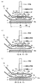
【解決手段】この欠陥修正方法では、ドレイン線8の断線欠陥部8bを含む範囲に修正ペースト20を塗布し、両端部がドレイン線8の正常な部分に重なる修正層20Aを形成し、修正層20Aにレーザ光を照射して焼成するステップを複数回繰り返し、断線欠陥部8bの上に複数の焼成層20Aを積層する。したがって、修正部の膜厚を厚くして修正部の抵抗値の低減化を図ることができる。
【選択図】図4
Description
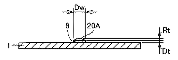
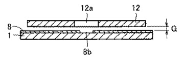
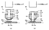
また好ましくは、第1のステップでは、フィルムに開けられた孔の開口部を断線欠陥部に隙間を開けて対峙させ、孔を含む所定の範囲でフィルムを基板に押圧するとともに孔を介して断線欠陥部を含む範囲に修正ペーストを塗布する。
また好ましくは、複数回の第1のステップにおいて同じ孔を使用する。
Claims (13)
- 基板上に形成された配線の断線欠陥部を修正する欠陥修正方法において、
前記断線欠陥部を含む範囲に修正ペーストを塗布して修正層を形成する第1のステップを含み、
前記修正層は、その両端部が前記配線の正常な部分に重なるように形成され、
前記第1のステップを複数回繰り返して前記断線欠陥部を含む範囲の上に複数の前記修正層を積層することを特徴とする、欠陥修正方法。 - 前記修正層にレーザ光を照射して前記修正層を焼成する第2のステップを含み、
前記第1および第2のステップを交互に繰り返すことを特徴とする、請求項1に記載の欠陥修正方法。 - 積層された前記複数の修正層にレーザ光を照射して前記複数の修正層を焼成する第2のステップを含むことを特徴とする、請求項1に記載の欠陥修正方法。
- 前記第1のステップでは、前記修正層を形成した後に前記修正層を乾燥させることを特徴とする、請求項1から請求項3までのいずれかに記載の欠陥修正方法。
- 前記第1のステップでは、フィルムに開けられた孔の開口部を前記断線欠陥部に隙間を開けて対峙させ、前記孔を含む所定の範囲で前記フィルムを前記基板に押圧するとともに前記孔を介して前記断線欠陥部を含む範囲に前記修正ペーストを塗布することを特徴とする、請求項1から請求項4までのいずれかに記載の欠陥修正方法。
- 各第1のステップにおいて未使用の前記孔を使用することを特徴とする、請求項5に記載の欠陥修正方法。
- 複数回の前記第1のステップにおいて同じ前記孔を使用することを特徴とする、請求項5に記載の欠陥修正方法。
- 複数回の前記第1のステップにおいて、前記フィルムの復元力で前記フィルムが前記基板から引き離された状態で、前記孔と前記断線欠陥部の相対位置を変更しないことを特徴とする、請求項7に記載の欠陥修正方法。
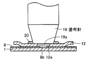
- 前記第1のステップでは、前記修正ペーストが付着した塗布針の先端部で前記孔を含む所定の範囲で前記フィルムを前記基板に押圧するとともに前記孔を介して前記断線欠陥部に前記修正ペーストを塗布した後、前記塗布針を上方に退避させ、前記フィルムの復元力で前記フィルムを前記基板から引き離すことを特徴とする、請求項5から請求項8までのいずれかに記載の欠陥修正方法。
- 2回目以降の前記第1のステップでは、前記塗布針の先端部に前記修正ペーストを補給しないことを特徴とする、請求項9に記載の欠陥修正方法。
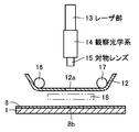
- 前記第1のステップでは、帯状の前記フィルムを折り返して上下に配置し、上方フィルムにレーザ光を照射して前記孔を形成し、前記フィルムを巻き取って前記孔を下方フィルムに位置させるとともに前記下方フィルムを前記基板の上方に配置し、前記下方フィルムの上に前記塗布針を配置することを特徴とする、請求項9または請求項10に記載の欠陥修正方法。
- さらに、前記下方フィルムの上に前記塗布針を配置する前に、前記上方フィルムの一部を移動させて前記下方フィルムに開けられた前記孔を露出させることを特徴とする、請求項11に記載の欠陥修正方法。
- 前記基板はTFT基板であることを特徴とする、請求項1から請求項12までのいずれかに記載の欠陥修正方法。
Priority Applications (1)
| Application Number | Priority Date | Filing Date | Title |
|---|---|---|---|
| JP2007258566A JP5051643B2 (ja) | 2007-10-02 | 2007-10-02 | 欠陥修正方法 |
Applications Claiming Priority (1)
| Application Number | Priority Date | Filing Date | Title |
|---|---|---|---|
| JP2007258566A JP5051643B2 (ja) | 2007-10-02 | 2007-10-02 | 欠陥修正方法 |
Publications (2)
| Publication Number | Publication Date |
|---|---|
| JP2009086500A true JP2009086500A (ja) | 2009-04-23 |
| JP5051643B2 JP5051643B2 (ja) | 2012-10-17 |
Family
ID=40659960
Family Applications (1)
| Application Number | Title | Priority Date | Filing Date |
|---|---|---|---|
| JP2007258566A Expired - Fee Related JP5051643B2 (ja) | 2007-10-02 | 2007-10-02 | 欠陥修正方法 |
Country Status (1)
| Country | Link |
|---|---|
| JP (1) | JP5051643B2 (ja) |
Cited By (1)
| Publication number | Priority date | Publication date | Assignee | Title |
|---|---|---|---|---|
| CN107006129A (zh) * | 2014-10-23 | 2017-08-01 | Ntn株式会社 | 基板的缺陷修正装置和缺陷修正方法、以及基板的缺陷修正部结构 |
Citations (13)
| Publication number | Priority date | Publication date | Assignee | Title |
|---|---|---|---|---|
| JPH04142702A (ja) * | 1990-10-04 | 1992-05-15 | Noritake Co Ltd | 抵抗値の修正方法 |
| JPH08203898A (ja) * | 1995-01-30 | 1996-08-09 | Hitachi Ltd | 電子回路基板の配線修正方法及びその装置並びに電子回路基板 |
| JPH08292442A (ja) * | 1995-04-24 | 1996-11-05 | Ntn Corp | 液晶基板の欠陥修正方法および欠陥修正装置 |
| JPH11108848A (ja) * | 1997-09-30 | 1999-04-23 | Ntn Corp | ペースト塗布修正装置 |
| JP2003098336A (ja) * | 2001-09-25 | 2003-04-03 | Seiko Epson Corp | カラーフィルタとその製造方法および装置、ならびに電気光学装置 |
| JP2003215640A (ja) * | 2002-10-17 | 2003-07-30 | Hitachi Ltd | Tft基板及びその配線修正方法並びに液晶表示装置 |
| JP2005095971A (ja) * | 2003-08-20 | 2005-04-14 | Lasertec Corp | パターン基板の欠陥修正方法及び欠陥修正装置並びにパターン基板製造方法 |
| JP2005300940A (ja) * | 2004-04-13 | 2005-10-27 | Sharp Corp | 基板リペア方法並びにリペア装置及びこれを用いてリペアされた基板 |
| JP2005317802A (ja) * | 2004-04-28 | 2005-11-10 | Lasertec Corp | パターン基板の欠陥修正方法及び欠陥修正装置並びにパターン基板製造方法 |
| JP2006276188A (ja) * | 2005-03-28 | 2006-10-12 | Ntn Corp | パターン修正装置およびパターン修正方法 |
| JP2007066800A (ja) * | 2005-09-01 | 2007-03-15 | Ntn Corp | パターン修正方法およびパターン修正装置 |
| JP2007165013A (ja) * | 2005-12-09 | 2007-06-28 | Ntn Corp | パターン欠陥修正方法およびパターン欠陥修正装置 |
| JP2007220894A (ja) * | 2006-02-16 | 2007-08-30 | Ntn Corp | パターン修正装置および修正液霧化ユニット |
-
2007
- 2007-10-02 JP JP2007258566A patent/JP5051643B2/ja not_active Expired - Fee Related
Patent Citations (14)
| Publication number | Priority date | Publication date | Assignee | Title |
|---|---|---|---|---|
| JPH04142702A (ja) * | 1990-10-04 | 1992-05-15 | Noritake Co Ltd | 抵抗値の修正方法 |
| JPH08203898A (ja) * | 1995-01-30 | 1996-08-09 | Hitachi Ltd | 電子回路基板の配線修正方法及びその装置並びに電子回路基板 |
| JPH08292442A (ja) * | 1995-04-24 | 1996-11-05 | Ntn Corp | 液晶基板の欠陥修正方法および欠陥修正装置 |
| JP2983879B2 (ja) * | 1995-04-24 | 1999-11-29 | エヌティエヌ株式会社 | 基板の欠陥修正方法および欠陥修正装置 |
| JPH11108848A (ja) * | 1997-09-30 | 1999-04-23 | Ntn Corp | ペースト塗布修正装置 |
| JP2003098336A (ja) * | 2001-09-25 | 2003-04-03 | Seiko Epson Corp | カラーフィルタとその製造方法および装置、ならびに電気光学装置 |
| JP2003215640A (ja) * | 2002-10-17 | 2003-07-30 | Hitachi Ltd | Tft基板及びその配線修正方法並びに液晶表示装置 |
| JP2005095971A (ja) * | 2003-08-20 | 2005-04-14 | Lasertec Corp | パターン基板の欠陥修正方法及び欠陥修正装置並びにパターン基板製造方法 |
| JP2005300940A (ja) * | 2004-04-13 | 2005-10-27 | Sharp Corp | 基板リペア方法並びにリペア装置及びこれを用いてリペアされた基板 |
| JP2005317802A (ja) * | 2004-04-28 | 2005-11-10 | Lasertec Corp | パターン基板の欠陥修正方法及び欠陥修正装置並びにパターン基板製造方法 |
| JP2006276188A (ja) * | 2005-03-28 | 2006-10-12 | Ntn Corp | パターン修正装置およびパターン修正方法 |
| JP2007066800A (ja) * | 2005-09-01 | 2007-03-15 | Ntn Corp | パターン修正方法およびパターン修正装置 |
| JP2007165013A (ja) * | 2005-12-09 | 2007-06-28 | Ntn Corp | パターン欠陥修正方法およびパターン欠陥修正装置 |
| JP2007220894A (ja) * | 2006-02-16 | 2007-08-30 | Ntn Corp | パターン修正装置および修正液霧化ユニット |
Cited By (1)
| Publication number | Priority date | Publication date | Assignee | Title |
|---|---|---|---|---|
| CN107006129A (zh) * | 2014-10-23 | 2017-08-01 | Ntn株式会社 | 基板的缺陷修正装置和缺陷修正方法、以及基板的缺陷修正部结构 |
Also Published As
| Publication number | Publication date |
|---|---|
| JP5051643B2 (ja) | 2012-10-17 |
Similar Documents
| Publication | Publication Date | Title |
|---|---|---|
| JP2012124381A (ja) | 塗布装置、塗布方法、およびパターン修正装置 | |
| JP2008192901A (ja) | パターン修正装置およびそれに用いられる塗布ユニット | |
| JP5051643B2 (ja) | 欠陥修正方法 | |
| JP4942430B2 (ja) | パターン修正方法およびパターン修正装置 | |
| JP5090038B2 (ja) | パターン修正装置およびパターン修正方法 | |
| JP2009291735A (ja) | 液状材料塗布方法と、液状材料塗布機構およびそれを用いた欠陥修正装置 | |
| KR101392554B1 (ko) | 패턴 수정 방법 및 패턴 수정 장치 | |
| JP2007038202A (ja) | パターン修正方法およびパターン修正装置 | |
| JP5035794B2 (ja) | パターン修正方法 | |
| JP5035799B2 (ja) | 欠陥修正方法 | |
| JP4987435B2 (ja) | 欠陥修正方法および欠陥修正装置 | |
| TWI421916B (zh) | A pattern correction method and a pattern correction device | |
| JP4993495B2 (ja) | パターン修正方法およびパターン修正装置 | |
| JP2009086499A (ja) | 欠陥修正方法 | |
| JP4925780B2 (ja) | パターン修正方法およびパターン修正装置 | |
| JP4904168B2 (ja) | パターン修正方法およびパターン修正装置 | |
| JP2008089668A (ja) | パターン修正方法およびパターン修正装置 | |
| JP2008281603A (ja) | パターン修正方法 | |
| JP2008039977A (ja) | パターン修正方法およびパターン修正装置 | |
| KR20080087668A (ko) | 패턴 수정 장치 및 패턴 수정 방법 | |
| JP2010085967A (ja) | パターン修正方法およびパターン修正装置 | |
| JP2012108246A (ja) | パターン修正方法 | |
| JP2008020603A (ja) | パターン修正方法およびパターン修正装置 | |
| JP2008288264A (ja) | パターン修正方法 | |
| JP2009103965A (ja) | 欠陥修正方法 |
Legal Events
| Date | Code | Title | Description |
|---|---|---|---|
| A621 | Written request for application examination |
Free format text: JAPANESE INTERMEDIATE CODE: A621 Effective date: 20100906 |
|
| A977 | Report on retrieval |
Free format text: JAPANESE INTERMEDIATE CODE: A971007 Effective date: 20120411 |
|
| A131 | Notification of reasons for refusal |
Free format text: JAPANESE INTERMEDIATE CODE: A131 Effective date: 20120417 |
|
| A521 | Written amendment |
Free format text: JAPANESE INTERMEDIATE CODE: A523 Effective date: 20120607 |
|
| TRDD | Decision of grant or rejection written | ||
| A01 | Written decision to grant a patent or to grant a registration (utility model) |
Free format text: JAPANESE INTERMEDIATE CODE: A01 Effective date: 20120626 |
|
| A01 | Written decision to grant a patent or to grant a registration (utility model) |
Free format text: JAPANESE INTERMEDIATE CODE: A01 |
|
| A61 | First payment of annual fees (during grant procedure) |
Free format text: JAPANESE INTERMEDIATE CODE: A61 Effective date: 20120717 |
|
| R150 | Certificate of patent or registration of utility model |
Free format text: JAPANESE INTERMEDIATE CODE: R150 |
|
| FPAY | Renewal fee payment (event date is renewal date of database) |
Free format text: PAYMENT UNTIL: 20150803 Year of fee payment: 3 |
|
| LAPS | Cancellation because of no payment of annual fees |