JP2009088018A - Stage control method, stage control apparatus, exposure method, exposure apparatus, and device manufacturing method - Google Patents
Stage control method, stage control apparatus, exposure method, exposure apparatus, and device manufacturing method Download PDFInfo
- Publication number
- JP2009088018A JP2009088018A JP2007252347A JP2007252347A JP2009088018A JP 2009088018 A JP2009088018 A JP 2009088018A JP 2007252347 A JP2007252347 A JP 2007252347A JP 2007252347 A JP2007252347 A JP 2007252347A JP 2009088018 A JP2009088018 A JP 2009088018A
- Authority
- JP
- Japan
- Prior art keywords
- stage
- drive signal
- stage control
- wafer
- control method
- Prior art date
- Legal status (The legal status is an assumption and is not a legal conclusion. Google has not performed a legal analysis and makes no representation as to the accuracy of the status listed.)
- Pending
Links
Images




Landscapes
- Container, Conveyance, Adherence, Positioning, Of Wafer (AREA)
- Exposure Of Semiconductors, Excluding Electron Or Ion Beam Exposure (AREA)
- Exposure And Positioning Against Photoresist Photosensitive Materials (AREA)
Abstract
【課題】基板の表面位置及び姿勢の制御を高精度に維持する。
【解決手段】第1駆動信号により第1方向に駆動されるとともに、第2駆動信号により第1方向と交差する第2方向に駆動されるステージWTBを制御する。第2駆動信号に基づいて、第1駆動信号を補正する補正ステップを有する。
【選択図】図4Control of the surface position and posture of a substrate is maintained with high accuracy.
A stage WTB driven in a first direction by a first drive signal and driven in a second direction intersecting the first direction by a second drive signal is controlled. A correction step of correcting the first drive signal based on the second drive signal is provided.
[Selection] Figure 4
Description
本発明は、ステージ制御方法、ステージ制御装置、露光方法及び露光装置並びにデバイス製造方法に関するものである。 The present invention relates to a stage control method, a stage control apparatus, an exposure method, an exposure apparatus, and a device manufacturing method.
半導体素子、液晶表示素子、CCD(Charge Coupled Device)等の撮像素子、薄膜磁気ヘッド、その他の各種デバイスの製造工程の1つとして設けられるフォトリソグラフィ工程では、マスク又はレチクル(以下、これらを総称する場合にはマスクという)に形成されたパターンを、投影光学系を介してフォトレジストが塗布されたガラスプレート又はウエハ等の基板に転写する露光装置が用いられている。 In a photolithography process provided as one of manufacturing processes of an image sensor such as a semiconductor element, a liquid crystal display element, a CCD (Charge Coupled Device), a thin film magnetic head, and other various devices, a mask or a reticle (hereinafter, these are collectively referred to) In some cases, an exposure apparatus is used that transfers a pattern formed on a mask) to a substrate such as a glass plate or a wafer coated with a photoresist via a projection optical system.
この種の露光装置では、基板を保持するホルダを基板ステージが支持した状態で移動することにより、基板を予め設定された露光位置へ移動させた後で、移動による振動が収まった(整定した)状態になった後でマスクに露光光を照射してマスクのパターンの転写を行っている。 In this type of exposure apparatus, by moving the holder that holds the substrate while the substrate stage is supported, the vibration caused by the movement is settled (settling) after the substrate is moved to a preset exposure position. After reaching the state, the mask pattern is transferred by irradiating the mask with exposure light.
リニアモータ等の駆動装置を用いて基板ステージを移動させると、基板ステージの機械的な特性により基板の表面方向の位置又は基板の姿勢(傾き)の変化が生ずることがある。このような変化が生ずると、基板内の位置に応じて投影光学系の像面に対する基板表面の位置関係が変化するため、パターンを忠実に転写することができなくなることがある。そこで、特許文献1には、基板ステージに対してホルダ(すなわち基板)を6自由度で駆動することにより、基板の表面位置及び姿勢を制御する技術が開示されている。
しかしながら、上述したような従来技術には、以下のような問題が存在する。
駆動装置を用いて基板ステージを移動させる際には、モータの漏れ推力により投影光学系の光軸方向にも力が生じることがある。
この場合、漏れ推力による力が外乱として加わることにより、上述した基板の表面位置及び姿勢に誤差が生じ、パターンの転写精度が低下する可能性がある。
However, the following problems exist in the conventional technology as described above.
When the substrate stage is moved using the driving device, a force may be generated in the optical axis direction of the projection optical system due to the leakage thrust of the motor.
In this case, when the force due to the leakage thrust is applied as a disturbance, an error occurs in the surface position and posture of the substrate described above, and the pattern transfer accuracy may decrease.
本発明は、以上のような点を考慮してなされたもので、基板の表面位置及び姿勢の制御を高精度に維持できるステージ制御方法、ステージ制御装置、露光方法及び露光装置並びにデバイス製造方法を提供することを目的とする。 The present invention has been made in consideration of the above points, and provides a stage control method, a stage control apparatus, an exposure method, an exposure apparatus, and a device manufacturing method capable of maintaining the control of the substrate surface position and orientation with high accuracy. The purpose is to provide.
上記の目的を達成するために本発明は、実施の形態を示す図1ないし図7に対応付けした以下の構成を採用している。
本発明のステージ制御方法は、第1駆動信号により第1方向に駆動されるとともに、第2駆動信号により前記第1方向と交差する第2方向に駆動されるステージ(WST)を制御するステージ制御方法であって、第2駆動信号に基づいて、第1駆動信号を補正する補正ステップを有することを特徴とするものである。
In order to achieve the above object, the present invention adopts the following configuration corresponding to FIGS. 1 to 7 showing the embodiment.
The stage control method of the present invention is a stage control for controlling a stage (WST) driven in a first direction by a first drive signal and driven in a second direction intersecting the first direction by a second drive signal. The method includes a correction step of correcting the first drive signal based on the second drive signal.
また、本発明のステージ制御装置は、第1駆動信号により第1方向に駆動されるとともに、第2駆動信号により前記第1方向と交差する第2方向に駆動されるステージ(WST)を制御するステージ制御装置であって、第2駆動信号に基づいて、第1駆動信号を補正する補正部(72)を有することを特徴とするものである。
従って、本発明のステージ制御方法及びステージ制御装置では、ステージ(WST)を第2方向に駆動する際に、当該ステージに加わる第1方向の力を第2駆動信号に基づいて算出し、算出した結果に応じて第1駆動信号を補正することにより、漏れ推力等の外乱による力が加わる際にも、この外乱を相殺するようにステージ(WST)を第1方向に駆動することが可能になる。
The stage controller of the present invention controls a stage (WST) driven in the first direction by the first drive signal and driven in the second direction intersecting the first direction by the second drive signal. The stage control device includes a correction unit (72) that corrects the first drive signal based on the second drive signal.
Therefore, in the stage control method and the stage control apparatus of the present invention, when the stage (WST) is driven in the second direction, the force in the first direction applied to the stage is calculated based on the second drive signal. By correcting the first drive signal according to the result, the stage (WST) can be driven in the first direction so as to cancel the disturbance even when a force such as a leakage thrust is applied due to the disturbance. .
また、本発明の露光方法は、先に記載のステージ制御方法を用いることを特徴とするものである。
さらに、本発明の露光装置は、先に記載のステージ制御装置を備えることを特徴とするものである。
従って、本発明の露光方法及び露光装置では、ステージ(WST)に保持された基板(W)の表面を所定の位置及び姿勢に制御することが可能になり、パターンの転写精度を高精度に維持することができる。
The exposure method of the present invention is characterized by using the stage control method described above.
Furthermore, the exposure apparatus of the present invention is characterized by including the stage control device described above.
Therefore, in the exposure method and exposure apparatus of the present invention, the surface of the substrate (W) held on the stage (WST) can be controlled to a predetermined position and posture, and the pattern transfer accuracy is maintained with high accuracy. can do.
そして、本発明のデバイス製造方法は、先に記載のステージ制御方法を用いることを特徴とするものである。
従って、本発明のデバイス製造では、パターンが基板に高精度で転写された高品質のデバイスを製造することが可能になる。
And the device manufacturing method of this invention uses the stage control method described previously, It is characterized by the above-mentioned.
Therefore, in the device manufacturing of the present invention, it is possible to manufacture a high-quality device in which the pattern is transferred to the substrate with high accuracy.
なお、本発明をわかりやすく説明するために、一実施例を示す図面の符号に対応付けて説明したが、本発明が実施例に限定されるものではないことは言うまでもない。 In order to explain the present invention in an easy-to-understand manner, the description has been made in association with the reference numerals of the drawings showing one embodiment, but it goes without saying that the present invention is not limited to the embodiment.
本発明では、基板の表面位置及び姿勢の制御を高精度に維持でき、パターンの転写精度を向上させることが可能になる。 In the present invention, the control of the surface position and posture of the substrate can be maintained with high accuracy, and the pattern transfer accuracy can be improved.
以下、本発明のステージ制御方法、ステージ制御装置、露光方法及び露光装置並びにデバイス製造方法の実施の形態を、図1ないし図9を参照して説明する。
ここでは、例えば、ステッパー等の一括露光型の投影露光装置に本発明を適用したものとして説明する。なお、以下の説明に用いる各図面では、各部材を認識可能な大きさとするため、各部材の縮尺を適宜変更している。
Embodiments of a stage control method, a stage control apparatus, an exposure method, an exposure apparatus, and a device manufacturing method according to the present invention will be described below with reference to FIGS.
Here, for example, description will be made assuming that the present invention is applied to a batch exposure type projection exposure apparatus such as a stepper. In each drawing used for the following description, the scale of each member is appropriately changed to make each member a recognizable size.
(露光装置の概略)
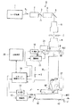
図1は、本例の投影露光装置を構成する各機能ユニットをブロック化して表した図であり、この図1において、投影露光装置を収納するチャンバーは省略されている。
図1において、露光用の光源としてKrFエキシマレーザ(波長248nm)又はArFエキシマレーザ(波長193nm)よりなるレーザ光源1が使用されている。その露光用の光源としては、その他のF2 レーザ(波長157nm)のような発振段階で紫外域のレーザ光を放射するもの、固体レーザ光源(YAG又は半導体レーザ等)からの近赤外域のレーザ光を波長変換して得られる真空紫外域の高調波レーザ光を放射するもの、或いはこの種の露光装置でよく使われている水銀放電ランプ等も使用できる。
(Outline of exposure equipment)
FIG. 1 is a block diagram showing functional units constituting the projection exposure apparatus of this example. In FIG. 1, the chamber for housing the projection exposure apparatus is omitted.
In FIG. 1, a laser light source 1 composed of a KrF excimer laser (wavelength 248 nm) or an ArF excimer laser (wavelength 193 nm) is used as a light source for exposure. As the light source for the exposure, other F2 lasers (wavelength 157 nm) such as those emitting laser light in the ultraviolet region at the oscillation stage, laser light in the near infrared region from a solid-state laser light source (such as YAG or semiconductor laser) It is also possible to use a lamp that emits high-frequency laser light in the vacuum ultraviolet region obtained by converting the wavelength of the above, or a mercury discharge lamp that is often used in this type of exposure apparatus.
レーザ光源1からの露光光源としての露光用の照明光(露光光)ILは、レンズ系とフライアイレンズ系とで構成される均一化光学系2、ビームスプリッタ3、光量調整用の可変減光器4、ミラー5、及びリレーレンズ系6を介してレチクルブラインド7を均一な照度分布で照射する。レチクルブラインド7で所定形状(一括露光型では例えば四角形、走査露光型では例えばスリット状)に制限された照明光ILは、結像レンズ系8を介してマスクとしてのレチクルR上に照射され、レチクルR上にはレチクルブラインド7の開口の像が結像される。均一化光学系2、ビームスプリッタ3、光量調整用の可変減光器4、ミラー5、リレーレンズ系6、レチクルブラインド7、及び結像レンズ系8を含んで照明光学系9が構成されている。
Illumination light (exposure light) IL for exposure as an exposure light source from the laser light source 1 is a uniformizing
レチクルRに形成された回路パターン領域(パターン)のうち、照明光によって照射される部分の像は、両側テレセントリックで投影倍率βが縮小倍率の投影光学系PLを介して基板(感応基板又は感光体)としてのフォトレジストが塗布されたウエハ(基板)W上に結像投影される。投影光学系PLは屈折系であるが、その他に反射屈折系等も使用できる。ウエハW以外にも液晶用のガラス基板、磁気ヘッド用のセラミック基板などが適用できる。以下、投影光学系PLの光軸AXに平行にZ軸を取り、Z軸に垂直な平面内で図1の紙面に平行な方向にX軸を、図1の紙面に垂直な方向にY軸を取って説明する。本実施形態における投影露光装置は一括型であるが、走査露光型の場合には、Y軸に沿った方向(Y方向)が、走査露光時のレチクルR及びウエハWの走査方向であり、レチクルR上の照明領域は、非走査方向であるX軸に沿った方向(X方向)に細長い形状となる。 Of the circuit pattern region (pattern) formed on the reticle R, the image of the portion irradiated with the illumination light is a two-sided telecentric substrate (a sensitive substrate or a photoreceptor) via a projection optical system PL with a projection magnification β of a reduction magnification. ) Is imaged and projected onto a wafer (substrate) W coated with a photoresist. Although the projection optical system PL is a refractive system, a catadioptric system or the like can also be used. In addition to the wafer W, a glass substrate for liquid crystal, a ceramic substrate for magnetic head, and the like can be applied. Hereinafter, the Z-axis is taken in parallel to the optical axis AX of the projection optical system PL, the X-axis is parallel to the plane of FIG. 1 in the plane perpendicular to the Z-axis, and the Y-axis is perpendicular to the plane of FIG. Take and explain. Although the projection exposure apparatus in the present embodiment is a collective type, in the case of the scanning exposure type, the direction along the Y axis (Y direction) is the scanning direction of the reticle R and the wafer W during scanning exposure, and the reticle. The illumination area on R has an elongated shape in a direction (X direction) along the X axis that is a non-scanning direction.
そして、投影光学系PLの物体面側に配置されるレチクルRは、レチクルステージRST(マスクステージ)に真空吸着等によって保持されている。レチクルステージRSTの移動座標位置(X方向、Y方向の位置、及びZ軸の周りの回転角)は、レチクルステージRSTに固定されたレチクル用移動鏡Mrと、投影光学系PLの上部側面に固定された参照鏡(不図示)と、これらに対向して配置されたレチクル用レーザ干渉計システム10とで逐次計測される。なお、レチクル用レーザ干渉計システム10は、実際には少なくともX方向に1軸及びY方向に2軸の3軸のレーザ干渉計を構成している。
The reticle R arranged on the object plane side of the projection optical system PL is held on the reticle stage RST (mask stage) by vacuum suction or the like. The movement coordinate position (X-direction, Y-direction position, and rotation angle around the Z-axis) of reticle stage RST is fixed to reticle moving mirror Mr fixed to reticle stage RST and the upper side surface of projection optical system PL. Measurement is performed sequentially with the reference mirror (not shown) and the reticle
また、レチクルステージRSTの移動は、リニアモータや微動アクチュエータ等で構成されるレチクル用駆動系11によって行われる。レチクル用レーザ干渉計システム10の計測情報はステージ制御ユニット14に供給され、ステージ制御ユニット14はその計測情報及び装置全体の動作を統轄制御するコンピュータよりなる主制御系20からの制御情報(入力情報)に基づいて、レチクル用駆動系11の動作を制御する。
In addition, movement of reticle stage RST is performed by reticle drive system 11 including a linear motor, a fine actuator, and the like. Measurement information of the reticle
一方、投影光学系PLの像面側に配置されるウエハWは、ウエハステージ(ステージ)WST上に真空吸着等によって保持されている。ウエハステージWSTは、ウエハWを吸着保持するウエハテーブルWTB(詳細後述)と、ウエハWのフォーカス位置(Z方向の位置)及びX軸、Y軸の周りの傾斜角を制御するためのZ駆動装置30a〜30c(詳細後述)とを含んでいる(図1では、ウエハステージWSTを簡略的に図示している)。 On the other hand, wafer W arranged on the image plane side of projection optical system PL is held on wafer stage (stage) WST by vacuum suction or the like. Wafer stage WST includes a wafer table WTB (details will be described later) for attracting and holding wafer W, and a Z drive device for controlling the focus position (position in the Z direction) of wafer W and the inclination angles around the X and Y axes. 30a to 30c (details will be described later). (In FIG. 1, wafer stage WST is simply illustrated).
一括露光型の場合には、ウエハステージWSTは、定盤Jのガイド面Ja上をX方向、Y方向にステップ移動する。走査露光型の場合には、ウエハステージWSTは、走査露光時に少なくともY方向に定速移動できるとともに、X方向及びY方向にステップ移動できるように、ガイド面Ja上に載置される。ウエハステージWSTの移動座標位置(X方向、Y方向の位置、及びZ軸の周りの回転角)は、投影光学系PLの下部に固定された参照鏡Mfと、ウエハステージWSTの反射面Mwと、これに対向して配置されたレーザ干渉計システム12とで逐次計測される。反射面Mw、参照鏡Mf、及びレーザ干渉計システム12は、実際には少なくともX方向に2軸及びY方向に1軸の3軸のレーザ干渉計を構成している。また、レーザ干渉計システム12は、実際にはさらにX軸及びY軸の周りの回転角(ヨーイング、ピッチング)計測用の2軸のレーザ干渉計も備えている。
In the case of the collective exposure type, wafer stage WST moves stepwise on guide surface Ja of surface plate J in the X and Y directions. In the case of the scanning exposure type, wafer stage WST is placed on guide surface Ja so that it can move at a constant speed in at least the Y direction and can move stepwise in the X and Y directions during scanning exposure. The movement coordinate position of wafer stage WST (the position in the X direction, the Y direction, and the rotation angle around the Z axis) includes a reference mirror Mf fixed to the lower part of projection optical system PL, and reflection surface Mw of wafer stage WST. The
また、投影光学系PLの下部側面に、斜入射方式の多点のオートフォーカスセンサ23A,23Bが固定されている。ステージ制御ユニット14は、そのスリット像の横ずれ量の情報を用いてそれら複数の計測点における投影光学系PLの像面からのデフォーカス量を算出し、露光時にはこれらのデフォーカス量が所定の制御精度内に収まるように、オートフォーカス方式でウエハステージWST内のZ駆動装置30a〜30cを駆動する。
Also, oblique incidence type
また、ステージ制御ユニット14は、レチクル用レーザ干渉計システム10による計測情報に基づいてレチクル用駆動系11を最適に制御するレチクル側のコントロール回路と、レーザ干渉計システム12による計測情報に基づいてウエハ用の駆動系13(詳細は後述する)を最適に制御するウエハ側のコントロール回路とを含んでいる。また、主制御系20は、ステージ制御ユニット14内の各コントロール回路と相互にコマンドやパラメータをやり取りして、オペレータが指定したプログラムに従って最適な露光処理を実行する。そのために、オペレータと主制御系20とのインターフェイスを成す不図示の操作パネルユニット(入力デバイスと表示デバイスとを含む)が設けられている。
The
さらに、露光に際しては、予めレチクルRとウエハWとのアライメントを行っておく必要がある。そこで、図1の投影露光装置には、レチクルRを所定位置に設定するためのレチクルアライメント系(RA系)21と、ウエハW上のマークを検出するためのオフアクシス方式のアライメント系22とが設けられている。
Furthermore, it is necessary to align the reticle R and the wafer W in advance for exposure. Therefore, the projection exposure apparatus of FIG. 1 includes a reticle alignment system (RA system) 21 for setting the reticle R at a predetermined position and an off-
図1において、一括露光型の場合には、照明光ILのもとでレチクルRのパターンを投影光学系PLを介してウエハW上の一つのショット領域に投影する動作と、ウエハステージWSTを介してウエハWをX方向、Y方向にステップ移動する動作とがステップ・アンド・リピート方式で繰り返されて、ウエハW上の全部のショット領域にレチクルRのパターン像が転写される。 In FIG. 1, in the case of the batch exposure type, an operation of projecting the pattern of the reticle R onto one shot area on the wafer W via the projection optical system PL under the illumination light IL, and the wafer stage WST. The operation of stepping and moving the wafer W in the X and Y directions is repeated by the step-and-repeat method, and the pattern image of the reticle R is transferred to all shot areas on the wafer W.
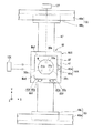
図2は、ウエハステージWSTの概略構成を示す平面図であり、図3はウエハステージWSTの正面図である。図2及び図3に示すように、ウェハステージWSTは、Y粗動ステージとしての移動ステージ41と、ウエハWを保持し移動ステージ41にZ駆動装置30a〜30cを介して支持される微動ステージとしてのウエハテーブルWTBとを備えている。移動ステージ41は、底面に設けられたエアベアリング42を介してガイド面Ja上をX方向、Y方向に移動自在に載置される。
FIG. 2 is a plan view showing a schematic configuration of wafer stage WST, and FIG. 3 is a front view of wafer stage WST. As shown in FIGS. 2 and 3, wafer stage WST is a moving
Z駆動装置30a〜30cは、移動ステージ41とウエハテーブルWTBとの間に、図2に示すように、三角形の頂点をなす位置に3箇所配置されており、それぞれが移動ステージ41に設けられた固定子43aと、ウエハテーブルWTBに設けられ固定子43aに対してZ方向に駆動される可動子43bとからなるボイスコイルモータで構成される。また、各可動子43bは、ステージ制御ユニット14の制御の下、それぞれ独立して駆動される。従って、Z駆動装置30a〜30cにおける可動子43bを同一量で駆動することにより、ウエハテーブルWTB(すなわちウエハW)をZ方向に移動させることができ、Z駆動装置30a〜30cにおける可動子43bの駆動量を異ならせることにより、ウエハテーブルWTB(すなわちウエハW)をθX方向(X軸周りの回転方向)及びθY方向(Y軸周りの回転方向)に移動させることができる。
As shown in FIG. 2, the
各Z駆動装置30a〜30cの近傍にはそれぞれ、各Z駆動装置30a〜30cのフォーカス方向(Z方向)の変位量を例えば0.01μm程度の分解能で計測できる高さセンサ31a〜31cがそれぞれ取り付けられている。高さセンサ31a〜31cの計測結果は、ステージ制御ユニット14に出力される。
また、ウエハステージWSTには、ウエハテーブルWTBを移動ステージ41に対してX方向に駆動するX駆動装置44Xと、ウエハテーブルWTBを移動ステージ41に対してY方向に駆動するY駆動装置44Y、44Yとが設けられている(図3では、Y駆動装置44Yは不図示)。X駆動装置44Xは、移動ステージ41に設けられた固定子45aと、ウエハテーブルWTBの+X側の側面に突設され固定子45aに対してX方向に駆動される可動子45bとからなるボイスコイルモータで構成される。同様に、各Y駆動装置44Yは、移動ステージ41に設けられた固定子46aと、ウエハテーブルWTBの−Y側の側面に突設され(図2参照)、固定子46aに対してY方向に駆動される可動子46bとからなるボイスコイルモータで構成され、X方向に間隔をあけて配置されている。
The wafer stage WST includes an
従って、X駆動装置44Xにおける可動子45bを駆動することにより、ウエハテーブルWTB(すなわちウエハW)をX方向に移動させることができ、Y駆動装置44Y、44Yにおける可動子46bを同一量で駆動することにより、ウエハテーブルWTB(すなわちウエハW)をY方向に移動させることができる。さらに、Y駆動装置44Y、44Yにおける可動子46bの駆動量または駆動方向を異ならせることにより、ウエハテーブルWTB(すなわちウエハW)をθZ方向(Z軸周りの回転方向)に移動させることができる。
Accordingly, by driving the
つまり、Z駆動装置30a〜30c、X駆動装置44X、Y駆動装置44Yの駆動を制御することにより、ウエハテーブルWTB(すなわちウエハW)を移動ステージ41に対して、Z方向、X方向、Y方向、θX方向、θY方向、θZ方向の6自由度で微小駆動することが可能となっている。
That is, by controlling the driving of the
また、ウエハステージWSTは、ウエハテーブルWTBと移動ステージ41との間をY軸方向に貫通するY軸ガイド47に沿ってY軸方向に移動自在に設けられている。そして、ウエハステージWSTは、Y軸ガイド47に設けられた固定子と、当該ウエハステージWSTに設けられた可動子とから構成される、例えばムービングマグネット型のY軸リニアモータ48によりY軸方向に長ストロークで移動する。また、ウエハステージWSTは、X軸方向に延在する固定子49aと、Y軸ガイド47の両端部に設けられた可動子49bとから構成される、例えばムービングコイル型のX軸リニアモータ50により、Y軸ガイド47を介してX軸方向に長ストロークで移動する。このとき、可動子49b、49bの移動量及び移動方向を同一とすることで、ウエハテーブルWTB(すなわちウエハW)をX軸方向に移動させることができ、可動子49b、49bの移動量または移動方向を異ならせることにより、ウエハテーブルWTB(すなわちウエハW)をθZ方向に移動させることができる。
Wafer stage WST is provided so as to be movable in the Y-axis direction along Y-
これらY軸リニアモータ48及びX軸リニアモータ50の駆動もステージ制御ユニット14により制御される。
また、上記Z駆動装置30a〜30c、X駆動装置44X、Y駆動装置44Y、Y軸リニアモータ48及びX軸リニアモータ50により駆動系13が構成される。
The driving of the Y-axis
The
ウエハテーブルWTBの−X方向の鏡面加工された側面MwXには、レーザ干渉計12XからY方向に離れた2本のレーザビームが照射され、ウエハテーブルWTBの+Y方向の鏡面加工された側面MwYには、レーザ干渉計12Yからレーザビームが照射され、レーザ干渉計12X及び12Yによって、ウエハテーブルWTBのX方向、Y方向の座標、及びZ軸の周りの回転角が計測されている。レーザ干渉計12X,12Yが図1のレーザ干渉計システム12に対応している。
The mirror-processed side surface MwX of wafer table WTB is irradiated with two laser beams separated in the Y direction from
レーザ干渉計12X,12Yの計測情報等に基づいて、図1に示すステージ制御ユニット14が粗動機構(Y軸リニアモータ48、X軸リニアモータ50)及び微動機構(Z駆動装置30a〜30c、X駆動装置44X、Y駆動装置44Y)からなる駆動系13を駆動する。前者の粗動機構は、一括露光型及び走査露光型ではウエハテーブルWTBのステップ移動のために使用できるとともに、走査露光型ではさらに同期走査時のウエハテーブルWTBの定速移動のために使用できる。後者の微動機構は、一括露光型及び走査露光型ではウエハテーブルWTBの位置決め誤差を補正するために使用でき、走査露光型ではさらに走査露光時のウエハテーブルWTBの同期誤差を補正するために使用することもできる。
Based on the measurement information of the
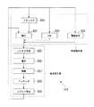
図4は、ウエハステージWSTに係るZ方向への駆動に関する制御系のブロック線図である。図4に示すように、ウエハテーブルWTBのZ方向の位置及び姿勢を制御する制御系は、フィードバック制御部70、フィードフォワード制御部71、XY駆動補正部(補正部)72、目標位置発生器73、演算部80〜82に大別される。フィードバック制御部70は、ローパスフィルタ、演算部、PI(Proportional Integral:比例積分)コントローラ等を含んで構成される。なお、本実施形態では、オートフォカスセンサ23A、23B及び高さセンサ31(31a〜31c)の検出結果を用いてフィードバック制御及びフィードフォワード制御を行うものとして説明するが、何れか一方の検出結果のみを用いてフィードバック制御を行ってもよい。
FIG. 4 is a block diagram of a control system related to driving in the Z direction according to wafer stage WST. As shown in FIG. 4, the control system for controlling the position and orientation of wafer table WTB in the Z direction includes a
目標位置発生器73は、ウエハステージWST(ウエハテーブルWTB)のZ方向(第1方向)の位置及び姿勢の目標値を与える基準信号を出力する。この目標位置発生器73は、主制御系20内に設けられる構成である。演算部80は、目標位置発生器73から出力された上記基準信号と、センサ(以下、オートフォカスセンサ23A、23B及び高さセンサ31(31a〜31c)を「センサ32」と称する)からの帰還信号との差分に応じた誤差信号を演算する。
フィードバック制御部70は、演算部80から出力される制御信号に基づいて、Z駆動装置30a〜30cを駆動するための制御信号(第1駆動信号)を生成するとともに、例えばウエハWの表面形状の急激な変化が生じている場合に、過剰な制御が行われて制御不能となるのを防止するために、演算部80から出力される信号の高周波成分をカットするフィルタリング処理を行う。
The
演算部81は、フィードバック制御部70から出力された制御信号に対してフィードフォワード制御部71から出力される制御信号を加算した制御信号を演算する。
フィードフォワード制御部71は、1つのショット領域に対する露光処理を終えてから次のショット領域に対する露光処理を行う際に行われるウエハステージWSTのX方向へのステップ移動によって生ずる露光中のウエハステージWSTのZ方向の位置を補正する補正量を発生する。これは、ステップ移動に伴って生ずる振動によってウエハWのZ方向の位置が変動してオートフォーカスエラーが生じる可能性があるためである。
この補正量は、ステップ長に応じて設定されるが、その詳細については、特願2004−200317等に記載されている。
The
The
This correction amount is set according to the step length, and details thereof are described in Japanese Patent Application No. 2004-200317.
演算部82は、演算部81から出力された制御信号(第1駆動信号)に対して、XY駆動補正部72から出力される制御信号を加算した制御信号を演算する。XY駆動補正部72は、X駆動装置44X、Y駆動装置44Y(適宜、駆動装置44と総称する)により、移動ステージ41に対してウエハテーブルWTBをX方向、Y方向に駆動した際に生じるZ方向への推力(いわゆる漏れ推力)を補正する制御信号(第2駆動信号)を出力する。
The
この漏れ推力は、駆動装置44がウエハテーブルWTBを駆動する際の加速度プロファイル(加速度の時間変化)に対して、1次の関数で表される関係で生じるものである。 This leakage thrust is generated by a relationship expressed by a linear function with respect to an acceleration profile (time change of acceleration) when the driving device 44 drives the wafer table WTB.
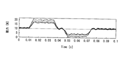
図5は、X駆動装置44XによりウエハテーブルWTBをX軸方向に駆動する際の推力プロファイル(すなわち加速度プロファイル)である。
また、図6は、X駆動装置44XによりウエハテーブルWTBをX軸方向に駆動した際にウエハテーブルWTBに加わるZ方向への推力プロファイル(すなわち加速度プロファイル)である。
FIG. 5 shows a thrust profile (that is, an acceleration profile) when the wafer table WTB is driven in the X-axis direction by the
FIG. 6 is a thrust profile (that is, an acceleration profile) in the Z direction applied to wafer table WTB when wafer table WTB is driven in the X-axis direction by
図5及び図6に示されるように、X軸方向への駆動の際のプロファイルと、Z軸方向へのプロファイルとは1次の相関関係を有している。
また、図6に示すプロファイルは、ウエハテーブルWTBのZ方向の位置に応じた異なるものとなっている。
従って、X駆動装置44Xの駆動に伴うウエハテーブルWTBのZ方向への加速度プロファイルFzは、X軸方向への加速度プロファイルFx、ウエハテーブルWTBのZ方向の位置Tzを用いて、次式で表される。
Fz=a×Fx×Tz+b …(1)
a、bは定数
As shown in FIGS. 5 and 6, the profile during driving in the X-axis direction and the profile in the Z-axis direction have a first-order correlation.
Further, the profile shown in FIG. 6 differs depending on the position of wafer table WTB in the Z direction.
Therefore, the acceleration profile Fz in the Z direction of the wafer table WTB accompanying the driving of the
Fz = a × Fx × Tz + b (1)
a and b are constants
上記の定数a、bは、予めX駆動装置44XによりウエハテーブルWTBをX軸方向に駆動した際に生じるZ軸方向の推力(加速度)を、ウエハテーブルWTBのZ位置を変えて計測することにより設定され記憶される。
そして、XY駆動補正部72は、センサ32で計測されたウエハテーブルWTBのZ位置、及び式(1)に基づいて求められる加速度プロファイルFzに応じて、この加速度(推力)を相殺するための制御信号を演算部82に出力する。
The above constants a and b are obtained by measuring the thrust (acceleration) in the Z-axis direction when the wafer table WTB is driven in the X-axis direction by the
Then, the XY
演算部82で演算された制御信号は、ウエハステージWST(ウエハテーブルWTB、Z駆動装置30a〜30c)に出力され、ウエハテーブルWTBのZ位置及び姿勢が制御される。
なお、上記の説明では、X駆動装置44Xの駆動に伴ってウエハテーブルWTBに生じるZ方向への推力について説明したが、実際には、XY駆動補正部72では、Y駆動装置44Yの駆動に伴ってウエハテーブルWTBに生じるZ方向への推力についても同様に求め、この推力を相殺する制御信号を出力する。
The control signal calculated by the
In the above description, the thrust in the Z direction generated in the wafer table WTB as the
以上、ウェハステージ37のZ方向の位置を補正する制御系の構成について説明したが、次に露光時の動作について簡単に説明する。
まず、露光処理を開始するにあたって、主制御系20は駆動系13を制御してウエハステージWSTをXY平面内でステップ移動させ、露光すべきショット領域を投影光学系PL(の投影領域)の直下に配置するとともに、ウエハWの表面を投影光学系PLの像面に一致させる。実際には、本実施形態では、上記ウエハステージWSTのステップ移動は、主にX軸リニアモータ50の駆動によるX軸方向に行われ、さらに、X軸方向のウエハテーブルWTBの高精度位置決め(ファインアライメント)は、X駆動装置44Xの駆動より行われる。
The configuration of the control system for correcting the position of the wafer stage 37 in the Z direction has been described above. Next, the operation during exposure will be briefly described.
First, when starting the exposure process, the
このウエハステージWSTのステップ移動に際しては、目標位置発生器73はウエハWのZ方向の位置及び姿勢の目標値を与える基準信号を出力する。目標位置発生器73から出力された基準信号は演算部80に入力し、演算部80において、センサからの帰還信号との差分に応じた誤差信号が演算され、フィードバック制御部70に出力される。
During step movement of wafer stage WST,
フィードバック制御部70に制御信号が入力すると、この制御信号に基づいてZ駆動装置30a〜30cを駆動するための制御信号が生成され、ローパスのフィルタリング処理が行われた後に演算部81に出力される。
When a control signal is input to the
このとき、フィードフォワード制御部71は、ステップ移動(例えばX方向へのステップ移動)に伴うウエハステージWST(ウエハテーブルWTB)のZ方向の位置を補正する補正量を発生し、演算部81に入力させる。そして、演算部81においては、フィードバック制御部70から出力されたZ駆動装置30a〜30cを駆動するための制御信号に、フィードフォワード制御部71が出力する制御信号(補正量)を加算(補正)し、演算部82に出力する。
At this time, the
演算部82に入力した制御信号に対しては、XY駆動補正部72から出力される制御信号が加算される。このXY駆動補正部72から出力される制御信号としては、センサ32で計測されたウエハWのZ方向の位置、及びX駆動装置44Xの駆動時の加速度プロファイルに応じて、上記式(1)で求められるZ方向への加速度プロファイルを補正する信号として、フィードフォワードで演算部82に出力される。
The control signal output from the XY
演算部82で演算・補正された制御信号は、ウエハステージWSTのステップ移動に伴って生じるX駆動装置44Xの駆動時に加わるZ方向への推力等の外乱要因が予めフィードフォワードで補正されているため、実際に外乱D(図4参照)が加わった後でも、これらの外乱要因による悪影響を排除(相殺)する駆動信号でZ駆動装置30a〜30cを駆動してウエハテーブルWTB(すなわちウエハW)のZ方向の位置及び姿勢が制御される。
In the control signal calculated and corrected by the
以上の制御は、ウエハW上のショット領域にステップ移動する毎に行われ、また、ステップ移動がX方向のみならず、Y方向や、X方向及びY方向の双方に移動する場合にも行われ、ステップ移動に伴って生ずる振動がオートフォーカスに悪影響を与えるのを防止することができる。 The above control is performed every time the step movement to the shot area on the wafer W is performed, and also when the step movement moves not only in the X direction but also in the Y direction or both the X direction and the Y direction. Thus, it is possible to prevent the vibration caused by the step movement from adversely affecting the autofocus.
以上説明したように、本実施形態では、ウエハステージWSTをステップ移動させる際に生じる漏れ推力等の外乱要因を、ウエハステージWSTの加速度情報に基づいてフィードフォワードで補正した駆動信号でZ駆動装置30a〜30c(ウエハテーブルWTB)を駆動するため、外乱に起因した誤差を排除した状態でウエハWの位置決めを実施でき、ウエハWの表面位置及び姿勢の制御を高精度に維持することが可能である。そのため、本実施形態では、ウエハWへのパターンの転写精度を高精度に維持することができる。
As described above, in the present embodiment, the
また、本実施形態では、ウエハテーブルWTBのZ方向の位置に対応する補正量を用いてZ駆動装置30a〜30cを駆動するため、ウエハテーブルWTBのZ位置毎に異なる誤差を精度よく補正することができる。
特に、本実施形態では、上記補正量がウエハテーブルWTBのZ位置に対して、1次の関数で表されることから、容易に補正量を設定できるとともに、精度よく補正量を設定することが可能である。
In the present embodiment, since the
In particular, in the present embodiment, since the correction amount is expressed by a linear function with respect to the Z position of the wafer table WTB, the correction amount can be easily set and the correction amount can be set with high accuracy. Is possible.
続いて、ステージ制御方法の第2実施形態について、図7を参照して説明する。
第2実施形態では、図4に示した制御ブロック図に対して、外乱オブザーバを用いた外乱補償器を付加し、リニアベアリングガイドの摩擦特性の変動等の外乱要因をキャンセルする構成としている。
なお、この図において、図4に示す第1実施形態の構成要素と同一の要素については同一符号を付し、その説明を省略する。
Next, a second embodiment of the stage control method will be described with reference to FIG.
In the second embodiment, a disturbance compensator using a disturbance observer is added to the control block diagram shown in FIG. 4 to cancel disturbance factors such as fluctuations in the friction characteristics of the linear bearing guide.
In this figure, the same components as those of the first embodiment shown in FIG. 4 are denoted by the same reference numerals, and the description thereof is omitted.
図7に示す外乱補償器90においては、まず、フィードバック制御部70から出力され、フィードフォワード制御部71が出力する制御信号が加算されたZ駆動装置30a〜30cを駆動するための制御信号を、2次低域通過型フィルタからなるフィルタ91により伝達関数Q(s)を用いてフィルタリングする。
一方、フィルタ92には、計測誤差nが加算されたセンサ32の計測結果が入力する。フィルタ92は、制御対象であるウエハステージWST(ウエハテーブルWTB)に対する伝達関数P(s)の逆モデル(伝達関数Pn(s))及び2次低域通過型フィルタ(Q(s))からなり、計測誤差nが加算されたセンサ32の計測結果より制御対象に印加されている実推力値指令値を推定する。
In the
On the other hand, the measurement result of the
そして、演算部93は、フィルタ91、92の差分をとることにより、外乱推定部として、制御対象であるウエハテーブルWTBに印加されている外乱力を推定し(外乱推定ステップ)、外乱補償信号生成部としての演算部94に出力する。演算部94は、この推定外乱力を演算部81が出力した制御信号に加算して、Z駆動装置30a〜30cを駆動するための制御信号を補償した外乱補償信号を生成する(外乱補償信号生成ステップ)。
And the calculating
このように、本実施形態では、上記第1実施形態と同様の作用・効果が得られることに加えて、制御ブロックに外乱オブザーバを付加することにより、ウエハステージWSTの駆動に伴う外乱要因(エアベアリング42の案内摩擦等)を推定して補償することが可能になり、特に低域での外乱要因を抑制することができる。この外乱オブザーバは、フィルタ91への入力が、XY駆動補正部72による補正前の信号であるため、XY駆動補正部72による補正が外乱として補償されてしまうことなく、確実に真の外乱要因による悪影響を抑制できる。
そのため、本実施形態では、ウエハテーブルWTBに保持されたウエハWの表面位置及び姿勢の制御をより高精度に維持することが可能である。
As described above, in this embodiment, in addition to obtaining the same operation and effect as those in the first embodiment, a disturbance observer (air) associated with driving of the wafer stage WST is added by adding a disturbance observer to the control block. It is possible to estimate and compensate the guide friction of the
Therefore, in this embodiment, it is possible to maintain the control of the surface position and posture of the wafer W held on the wafer table WTB with higher accuracy.
以上、添付図面を参照しながら本発明に係る好適な実施形態について説明したが、本発明は係る例に限定されないことは言うまでもない。上述した例において示した各構成部材の諸形状や組み合わせ等は一例であって、本発明の主旨から逸脱しない範囲において設計要求等に基づき種々変更可能である。 As described above, the preferred embodiments according to the present invention have been described with reference to the accompanying drawings, but the present invention is not limited to the examples. Various shapes, combinations, and the like of the constituent members shown in the above-described examples are examples, and various modifications can be made based on design requirements and the like without departing from the gist of the present invention.
例えば、上記実施形態では、ウエハテーブルWTBをX軸方向に移動させる際に生じるZ軸方向の推力を、X軸方向の加速度情報に基づいて補正するものとして説明したが、上述したように、Y軸方向(第3方向)に第3駆動信号により移動させる際の加速度情報に基づいて補正する方式や、X軸方向及びY軸方向の双方に移動させる際には、X軸方向及びY軸方向の双方の加速度情報に基づいて補正する方式としてもよい。さらに、上記実施形態では、Z軸方向に加わる推力を補正するものとして説明したが、これに限定されるものではなく、例えばウエハテーブルWTBをX軸方向に移動させる際の加速度情報に基づいて、Y軸方向に生じる推力を補正する構成や、Z軸方向に移動させる際の加速度情報に基づいて、Y軸方向に生じる推力やX軸方向に生じる推力を補正する構成としてもよい。すなわち、本発明は、3軸方向に移動可能なステージに対して、この中の第1軸と第2軸との少なくとも一つに移動する際の駆動信号(の加速度情報)に基づいて、第3軸に沿って生じる推力を補正することが可能である。 For example, in the above-described embodiment, the Z-axis direction thrust generated when the wafer table WTB is moved in the X-axis direction is corrected based on the acceleration information in the X-axis direction. Correction method based on acceleration information when moving in the axial direction (third direction) by the third drive signal, and when moving in both the X-axis direction and the Y-axis direction, the X-axis direction and the Y-axis direction It is good also as a system which correct | amends based on both acceleration information of these. Furthermore, in the above embodiment, the thrust applied in the Z-axis direction has been described as being corrected. However, the present invention is not limited to this. For example, based on acceleration information when moving the wafer table WTB in the X-axis direction, A configuration in which thrust generated in the Y-axis direction is corrected, or a configuration in which thrust generated in the Y-axis direction and thrust generated in the X-axis direction are corrected based on acceleration information when moving in the Z-axis direction may be employed. That is, the present invention is based on a drive signal (acceleration information thereof) when moving to at least one of the first axis and the second axis of a stage movable in three axis directions. It is possible to correct the thrust generated along the three axes.
なお、上記各実施形態の基板(物体)としては、半導体デバイス製造用の半導体ウエハのみならず、ディスプレイデバイス用のガラス基板や、薄膜磁気ヘッド用のセラミックウエハ、あるいは露光装置で用いられるマスクまたはレチクルの原版(合成石英、シリコンウエハ)等が適用される。 The substrate (object) in each of the above embodiments is not limited to a semiconductor wafer for manufacturing a semiconductor device, but a glass substrate for a display device, a ceramic wafer for a thin film magnetic head, or a mask or reticle used in an exposure apparatus. The original plate (synthetic quartz, silicon wafer) or the like is applied.
露光装置としては、レチクルRとウエハWとを静止した状態でレチクルRのパターンを一括露光し、ウエハWを順次ステップ移動させるステップ・アンド・リピート方式の投影露光装置(ステッパ)の他に、レチクルRとウエハWとを同期移動してレチクルRのパターンを走査露光するステップ・アンド・スキャン方式の走査型露光装置(スキャニングステッパ)にも適用することができる。また、本発明はウエハW上で少なくとも2つのパターンを部分的に重ねて転写するステップ・アンド・スティッチ方式の露光装置にも適用できる。 As the exposure apparatus, in addition to a step-and-repeat type projection exposure apparatus (stepper) that collectively exposes the pattern of the reticle R while the reticle R and the wafer W are stationary, and sequentially moves the wafer W stepwise, the reticle The present invention can also be applied to a step-and-scan type scanning exposure apparatus (scanning stepper) that scans and exposes the pattern of the reticle R by synchronously moving R and the wafer W. The present invention can also be applied to a step-and-stitch type exposure apparatus that partially transfers at least two patterns on the wafer W.
露光装置の種類としては、ウエハWに半導体素子パターンを露光する半導体素子製造用の露光装置に限られず、液晶表示素子製造用又はディスプレイ製造用の露光装置や、薄膜磁気ヘッド、撮像素子(CCD)あるいはレチクル又はマスクなどを製造するための露光装置などにも広く適用できる。 The type of exposure apparatus is not limited to an exposure apparatus for manufacturing a semiconductor element that exposes a semiconductor element pattern on the wafer W, but is an exposure apparatus for manufacturing a liquid crystal display element or a display, a thin film magnetic head, an image sensor (CCD). Alternatively, it can be widely applied to an exposure apparatus for manufacturing a reticle or a mask.
また、本発明が適用される露光装置の光源には、KrFエキシマレーザ(248nm)、ArFエキシマレーザ(193nm)、F2レーザ(157nm)等のみならず、g線(436nm)及びi線(365nm)を用いることができる。さらに、投影光学系の倍率は縮小系のみならず等倍および拡大系のいずれでもよい。また、上記実施形態では、反射屈折型の投影光学系を例示したが、これに限定されるものではなく、投影光学系の光軸(レチクル中心)と投影領域の中心とが異なる位置に設定される屈折型の投影光学系にも適用可能である。 The light source of the exposure apparatus to which the present invention is applied includes not only KrF excimer laser (248 nm), ArF excimer laser (193 nm), F 2 laser (157 nm), but also g-line (436 nm) and i-line (365 nm). ) Can be used. Further, the magnification of the projection optical system may be not only a reduction system but also an equal magnification or an enlargement system. In the above embodiment, the catadioptric projection optical system is exemplified, but the present invention is not limited to this, and the optical axis (reticle center) of the projection optical system and the center of the projection area are set at different positions. It can also be applied to a refraction type projection optical system.
また、本発明は、投影光学系と基板との間に局所的に液体を満たし、該液体を介して基板を露光する、所謂液浸露光装置に適用したが、液浸露光装置については、国際公開第99/49504号パンフレットに開示されている。さらに、本発明は、特開平6−124873号公報、特開平10−303114号公報、米国特許第5,825,043号などに開示されているような露光対象の基板の表面全体が液体中に浸かっている状態で露光を行う液浸露光装置にも適用可能である。 Further, the present invention is applied to a so-called immersion exposure apparatus in which a liquid is locally filled between the projection optical system and the substrate, and the substrate is exposed through the liquid. It is disclosed in the publication No. 99/49504 pamphlet. Further, in the present invention, the entire surface of the substrate to be exposed as disclosed in JP-A-6-124873, JP-A-10-303114, US Pat. No. 5,825,043 and the like is in the liquid. The present invention is also applicable to an immersion exposure apparatus that performs exposure while being immersed.
また、本発明は、基板ステージ(ウエハステージ)が複数設けられるツインステージ型の露光装置にも適用できる。ツインステージ型の露光装置の構造及び露光動作は、例えば特開平10−163099号公報及び特開平10−214783号公報(対応米国特許6,341,007号、6,400,441号、6,549,269号及び6,590,634号)、特表2000−505958号(対応米国特許5,969,441号)或いは米国特許6,208,407号に開示されている。更に、本発明を本願出願人が先に出願した特願2004−168481号のウエハステージに適用してもよい。 The present invention can also be applied to a twin stage type exposure apparatus provided with a plurality of substrate stages (wafer stages). The structure and exposure operation of a twin stage type exposure apparatus are described in, for example, Japanese Patent Laid-Open Nos. 10-163099 and 10-214783 (corresponding US Pat. Nos. 6,341,007, 6,400,441, 6,549). , 269 and 6,590,634), JP 2000-505958 (corresponding US Pat. No. 5,969,441) or US Pat. No. 6,208,407. Furthermore, the present invention may be applied to the wafer stage disclosed in Japanese Patent Application No. 2004-168482 filed earlier by the present applicant.
また、本発明が適用される露光装置は、本願特許請求の範囲に挙げられた各構成要素を含む各種サブシステムを、所定の機械的精度、電気的精度、光学的精度を保つように、組み立てることで製造される。これら各種精度を確保するために、この組み立ての前後には、各種光学系については光学的精度を達成するための調整、各種機械系については機械的精度を達成するための調整、各種電気系については電気的精度を達成するための調整が行われる。各種サブシステムから露光装置への組み立て工程は、各種サブシステム相互の、機械的接続、電気回路の配線接続、気圧回路の配管接続等が含まれる。この各種サブシステムから露光装置への組み立て工程の前に、各サブシステム個々の組み立て工程があることはいうまでもない。各種サブシステムの露光装置への組み立て工程が終了したら、総合調整が行われ、露光装置全体としての各種精度が確保される。なお、露光装置の製造は温度およびクリーン度等が管理されたクリーンルームで行うことが望ましい。 An exposure apparatus to which the present invention is applied assembles various subsystems including the constituent elements recited in the claims of the present application so as to maintain predetermined mechanical accuracy, electrical accuracy, and optical accuracy. It is manufactured by. In order to ensure these various accuracies, before and after assembly, various optical systems are adjusted to achieve optical accuracy, various mechanical systems are adjusted to achieve mechanical accuracy, and various electrical systems are Adjustments are made to achieve electrical accuracy. The assembly process from the various subsystems to the exposure apparatus includes mechanical connection, electrical circuit wiring connection, pneumatic circuit piping connection and the like between the various subsystems. Needless to say, there is an assembly process for each subsystem before the assembly process from the various subsystems to the exposure apparatus. When the assembly process of the various subsystems to the exposure apparatus is completed, comprehensive adjustment is performed to ensure various accuracies as the entire exposure apparatus. The exposure apparatus is preferably manufactured in a clean room where the temperature, cleanliness, etc. are controlled.
次に、本発明の実施形態による露光装置及び露光方法をリソグラフィ工程で使用したマイクロデバイスの製造方法の実施形態について説明する。図8は、マイクロデバイス(ICやLSI等の半導体チップ、液晶パネル、CCD、薄膜磁気ヘッド、マイクロマシン等)の製造例のフローチャートを示す図である。
まず、ステップS10(設計ステップ)において、マイクロデバイスの機能・性能設計(例えば、半導体デバイスの回路設計等)を行い、その機能を実現するためのパターン設計を行う。引き続き、ステップS11(マスク製作ステップ)において、設計した回路パターンを形成したマスク(レチクル)を製作する。一方、ステップS12(ウエハ製造ステップ)において、シリコン等の材料を用いてウエハを製造する。
次に、ステップS13(ウエハ処理ステップ)において、ステップS10〜ステップS12で用意したマスクとウエハを使用して、後述するように、リソグラフィ技術等によってウエハ上に実際の回路等を形成する。次いで、ステップS14(デバイス組立ステップ)において、ステップS13で処理されたウエハを用いてデバイス組立を行う。このステップS14には、ダイシング工程、ボンティング工程、及びパッケージング工程(チップ封入)等の工程が必要に応じて含まれる。最後に、ステップS15(検査ステップ)において、ステップS14で作製されたマイクロデバイスの動作確認テスト、耐久性テスト等の検査を行う。こうした工程を経た後にマイクロデバイスが完成し、これが出荷される。
Next, an embodiment of a manufacturing method of a micro device using the exposure apparatus and the exposure method according to the embodiment of the present invention in the lithography process will be described. FIG. 8 is a flowchart showing a manufacturing example of a microdevice (a semiconductor chip such as an IC or LSI, a liquid crystal panel, a CCD, a thin film magnetic head, a micromachine, or the like).
First, in step S10 (design step), function / performance design (for example, circuit design of a semiconductor device) of a micro device is performed, and pattern design for realizing the function is performed. Subsequently, in step S11 (mask manufacturing step), a mask (reticle) on which the designed circuit pattern is formed is manufactured. On the other hand, in step S12 (wafer manufacturing step), a wafer is manufactured using a material such as silicon.
Next, in step S13 (wafer processing step), using the mask and wafer prepared in steps S10 to S12, an actual circuit or the like is formed on the wafer by lithography or the like, as will be described later. Next, in step S14 (device assembly step), device assembly is performed using the wafer processed in step S13. This step S14 includes processes such as a dicing process, a bonding process, and a packaging process (chip encapsulation) as necessary. Finally, in step S15 (inspection step), inspections such as an operation confirmation test and a durability test of the microdevice manufactured in step S14 are performed. After these steps, the microdevice is completed and shipped.
図9は、半導体デバイスの場合におけるステップS13の詳細工程の一例を示す図である。
ステップS21(酸化ステップ)おいては、ウエハの表面を酸化させる。ステップS22(CVDステップ)においては、ウエハ表面に絶縁膜を形成する。ステップS23(電極形成ステップ)においては、ウエハ上に電極を蒸着によって形成する。ステップS24(イオン打込みステップ)においては、ウエハにイオンを打ち込む。以上のステップS21〜ステップS24のそれぞれは、ウエハ処理の各段階の前処理工程を構成しており、各段階において必要な処理に応じて選択されて実行される。
ウエハプロセスの各段階において、上述の前処理工程が終了すると、以下のようにして後処理工程が実行される。この後処理工程では、まず、ステップS25(レジスト形成ステップ)において、ウエハに感光剤を塗布する。引き続き、ステップS26(露光ステップ)において、上で説明したリソグラフィシステム(露光装置)及び露光方法によってマスクの回路パターンをウエハに転写する。次に、ステップS27(現像ステップ)においては露光されたウエハを現像し、ステップS28(エッチングステップ)において、レジストが残存している部分以外の部分の露出部材をエッチングにより取り去る。そして、ステップS29(レジスト除去ステップ)において、エッチングが済んで不要となったレジストを取り除く。これらの前処理工程と後処理工程とを繰り返し行うことによって、ウエハ上に多重に回路パターンが形成される。
FIG. 9 is a diagram illustrating an example of a detailed process of step S13 in the case of a semiconductor device.
In step S21 (oxidation step), the surface of the wafer is oxidized. In step S22 (CVD step), an insulating film is formed on the wafer surface. In step S23 (electrode formation step), an electrode is formed on the wafer by vapor deposition. In step S24 (ion implantation step), ions are implanted into the wafer. Each of the above steps S21 to S24 constitutes a pre-processing process at each stage of the wafer processing, and is selected and executed according to a necessary process at each stage.
At each stage of the wafer process, when the above pre-process is completed, the post-process is executed as follows. In this post-processing process, first, in step S25 (resist formation step), a photosensitive agent is applied to the wafer. Subsequently, in step S26 (exposure step), the circuit pattern of the mask is transferred to the wafer by the lithography system (exposure apparatus) and the exposure method described above. Next, in step S27 (development step), the exposed wafer is developed, and in step S28 (etching step), exposed members other than the portion where the resist remains are removed by etching. In step S29 (resist removal step), the resist that has become unnecessary after the etching is removed. By repeatedly performing these pre-processing steps and post-processing steps, multiple circuit patterns are formed on the wafer.
また、半導体素子等のマイクロデバイスだけではなく、光露光装置、EUV露光装置、X線露光装置、及び電子線露光装置等で使用されるレチクル又はマスクを製造するために、マザーレチクルからガラス基板やシリコンウエハ等ヘ回路パターンを転写する露光装置にも本発明を適用できる。ここで、DUV(深紫外)やVUV(真空紫外)光等を用いる露光装置では、一般的に透過型レチクルが用いられ、レチクル基板としては石英ガラス、フッ素がドープされた石英ガラス、蛍石、フッ化マグネシウム、又は水晶等が用いられる。また、プロキシミティ方式のX線露光装置や電子線露光装置等では、透過型マスク(ステンシルマスク、メンブレンマスク)が用いられ、マスク基板としてはシリコンウエハ等が用いられる。なお、このような露光装置は、WO99/34255号、WO99/50712号、WO99/66370号、特開平11−194479号、特開2000−12453号、特開2000−29202号等に開示されている。 Further, in order to manufacture reticles or masks used in not only microdevices such as semiconductor elements but also light exposure apparatuses, EUV exposure apparatuses, X-ray exposure apparatuses, electron beam exposure apparatuses, etc., from mother reticles to glass substrates and The present invention can also be applied to an exposure apparatus that transfers a circuit pattern to a silicon wafer or the like. Here, in an exposure apparatus using DUV (deep ultraviolet), VUV (vacuum ultraviolet) light, or the like, a transmission type reticle is generally used. As a reticle substrate, quartz glass, fluorine-doped quartz glass, fluorite, Magnesium fluoride or quartz is used. In proximity-type X-ray exposure apparatuses, electron beam exposure apparatuses, and the like, a transmissive mask (stencil mask, membrane mask) is used, and a silicon wafer or the like is used as a mask substrate. Such an exposure apparatus is disclosed in WO99 / 34255, WO99 / 50712, WO99 / 66370, JP-A-11-194479, JP-A2000-12453, JP-A-2000-29202, and the like. .
Ja…ガイド面、 R…レチクル(マスク)、 W…ウエハ(基板)、 WST…ウエハステージ(ステージ)、 72…XY駆動補正部(補正部)、 93…演算部(外乱推定部)、 94…演算部(外乱補償信号生成部) Ja ... Guide surface, R ... Reticle (mask), W ... Wafer (substrate), WST ... Wafer stage (stage), 72 ... XY drive correction unit (correction unit), 93 ... Calculation unit (disturbance estimation unit), 94 ... Calculation unit (disturbance compensation signal generator)
Claims (19)
前記第2駆動信号に基づいて、前記第1駆動信号を補正する補正ステップを有するステージ制御方法。 A stage control method for controlling a stage driven in a first direction by a first drive signal and driven in a second direction intersecting the first direction by a second drive signal,
A stage control method comprising a correction step of correcting the first drive signal based on the second drive signal.
前記ステージの前記第1方向の位置に対応する補正量を用いて、前記第1駆動信号を補正するステージ制御方法。 The stage control method according to claim 1,
A stage control method for correcting the first drive signal using a correction amount corresponding to the position of the stage in the first direction.
前記補正量と前記ステージの前記第1方向の位置とは1次の関数で表せるステージ制御方法。 The stage control method according to claim 2, wherein
A stage control method in which the correction amount and the position of the stage in the first direction can be expressed by a linear function.
前記第2駆動信号に含まれる前記ステージの加速度情報を用いて、前記第1駆動信号を補正するステージ制御方法。 In the stage control method according to any one of claims 1 to 3,
A stage control method for correcting the first drive signal by using acceleration information of the stage included in the second drive signal.
前記第2駆動信号に基づく情報を前記第1駆動信号にフィードフォワードして前記ステージを前記第1方向へ駆動するステップを含むステージ制御方法。 In the stage control method according to any one of claims 1 to 4,
A stage control method including a step of feeding forward information based on the second drive signal to the first drive signal to drive the stage in the first direction.
前記ステージが前記第1方向へ駆動されたことで得られる情報に基づいて該ステージに加わる外乱を推定する外乱推定ステップと、
前記外乱推定ステップで求められた推定外乱に基づいて前記第1駆動信号を補償した外乱補償信号を生成する外乱補償信号生成ステップと、
を含み、前記外乱補償信号と前記第2駆動信号とに基づいてステージの駆動が行なわれるステージ制御方法。 In the stage control method according to any one of claims 1 to 5,
A disturbance estimation step of estimating a disturbance applied to the stage based on information obtained by driving the stage in the first direction;
A disturbance compensation signal generating step for generating a disturbance compensation signal in which the first drive signal is compensated based on the estimated disturbance obtained in the disturbance estimating step;
And a stage control method in which the stage is driven based on the disturbance compensation signal and the second drive signal.
前記ステージは、前記第2方向を含むガイド面に沿って移動し、
前記第1方向は、前記ガイド面と略直交する方向であるステージ制御方法。 In the stage control method according to any one of claims 1 to 6,
The stage moves along a guide surface including the second direction;
The stage control method, wherein the first direction is a direction substantially orthogonal to the guide surface.
前記ステージは、前記ガイド面内で前記第2方向と交差する第3方向に第3駆動信号により駆動され、
前記第3駆動信号に基づいて、前記第1駆動信号を補正するステップを有するステージ制御方法。 The stage control method according to claim 7, wherein
The stage is driven by a third drive signal in a third direction intersecting the second direction within the guide surface,
A stage control method comprising a step of correcting the first drive signal based on the third drive signal.
前記第2駆動信号に基づいて、前記第1駆動信号を補正する補正部を有するステージ制御装置。 A stage control device that controls a stage driven in a first direction by a first drive signal and driven in a second direction that intersects the first direction by a second drive signal,
A stage control apparatus comprising: a correction unit that corrects the first drive signal based on the second drive signal.
前記補正部は、前記ステージの前記第1方向の位置に対応する補正量を用いて、前記第1駆動信号を補正するステージ制御装置。 The stage control device according to claim 11, wherein
The correction unit is a stage control device that corrects the first drive signal using a correction amount corresponding to the position of the stage in the first direction.
前記補正量と前記ステージの前記第1方向の位置とは、1次の関数で表せるステージ制御装置。 The stage control apparatus according to claim 12, wherein
The stage control apparatus in which the correction amount and the position of the stage in the first direction can be expressed by a linear function.
前記補正部は、前記第2駆動信号に含まれる前記ステージの加速度情報を用いて、前記第1駆動信号を補正するステージ制御装置。 In the stage control device according to any one of claims 11 to 13,
The correction unit is a stage control device that corrects the first drive signal using acceleration information of the stage included in the second drive signal.
前記第2駆動信号に基づく情報を前記第1駆動信号にフィードフォワードして前記ステージを前記第1方向へ駆動するステージ制御装置。 In the stage control device according to any one of claims 11 to 14,
A stage controller that feeds information based on the second drive signal to the first drive signal to drive the stage in the first direction.
前記ステージが前記第1方向へ駆動されたことで得られる情報に基づいて該ステージに加わる外乱を推定する外乱推定部と、
前記外乱推定部で求められた推定外乱に基づいて前記第1駆動信号を補償した外乱補償信号を生成する外乱補償信号生成部とを含み、
前記外乱補償信号と前記第2駆動信号とに基づいて前記ステージの駆動を行なうステージ制御装置。 In the stage control device according to any one of claims 11 to 15,
A disturbance estimation unit that estimates a disturbance applied to the stage based on information obtained by driving the stage in the first direction;
A disturbance compensation signal generation unit that generates a disturbance compensation signal that compensates for the first drive signal based on the estimated disturbance obtained by the disturbance estimation unit;
A stage control device for driving the stage based on the disturbance compensation signal and the second drive signal.
前記ステージは、前記第2方向を含むガイド面に沿って移動し、
前記第1方向は、前記ガイド面と略直交する方向であるステージ制御装置。 In the stage control device according to any one of claims 11 to 16,
The stage moves along a guide surface including the second direction;
The stage control device, wherein the first direction is a direction substantially orthogonal to the guide surface.
前記ステージは、前記ガイド面内で前記第2方向と交差する第3方向に第3駆動信号により駆動され、
前記補正部は、前記第3駆動信号に基づいて、前記第1駆動信号を補正するステージ制御装置。 The stage control apparatus according to claim 17, wherein
The stage is driven by a third drive signal in a third direction intersecting the second direction within the guide surface,
The correction unit is a stage control device that corrects the first drive signal based on the third drive signal.
Priority Applications (1)
| Application Number | Priority Date | Filing Date | Title |
|---|---|---|---|
| JP2007252347A JP2009088018A (en) | 2007-09-27 | 2007-09-27 | Stage control method, stage control apparatus, exposure method, exposure apparatus, and device manufacturing method |
Applications Claiming Priority (1)
| Application Number | Priority Date | Filing Date | Title |
|---|---|---|---|
| JP2007252347A JP2009088018A (en) | 2007-09-27 | 2007-09-27 | Stage control method, stage control apparatus, exposure method, exposure apparatus, and device manufacturing method |
Publications (1)
| Publication Number | Publication Date |
|---|---|
| JP2009088018A true JP2009088018A (en) | 2009-04-23 |
Family
ID=40661101
Family Applications (1)
| Application Number | Title | Priority Date | Filing Date |
|---|---|---|---|
| JP2007252347A Pending JP2009088018A (en) | 2007-09-27 | 2007-09-27 | Stage control method, stage control apparatus, exposure method, exposure apparatus, and device manufacturing method |
Country Status (1)
| Country | Link |
|---|---|
| JP (1) | JP2009088018A (en) |
Cited By (5)
| Publication number | Priority date | Publication date | Assignee | Title |
|---|---|---|---|---|
| JP2010008956A (en) * | 2008-06-30 | 2010-01-14 | Yokohama National Univ | Stage device, exposure apparatus and stage control method |
| JP2012028784A (en) * | 2010-07-26 | 2012-02-09 | Asml Netherlands Bv | Position control system, lithographic apparatus, and method to control position of movable object |
| JP2013222962A (en) * | 2012-04-18 | 2013-10-28 | Asml Holding Nv | Lithography device and method of compensating for intrinsic mode coupling |
| US11630398B2 (en) | 2018-07-04 | 2023-04-18 | Canon Kabushiki Kaisha | Control apparatus, exposure apparatus, and method of manufacturing article |
| JP2023103762A (en) * | 2022-01-14 | 2023-07-27 | 株式会社ニューフレアテクノロジー | PATTERN INSPECTION APPARATUS AND PATTERN INSPECTION METHOD |
-
2007
- 2007-09-27 JP JP2007252347A patent/JP2009088018A/en active Pending
Cited By (8)
| Publication number | Priority date | Publication date | Assignee | Title |
|---|---|---|---|---|
| JP2010008956A (en) * | 2008-06-30 | 2010-01-14 | Yokohama National Univ | Stage device, exposure apparatus and stage control method |
| JP2012028784A (en) * | 2010-07-26 | 2012-02-09 | Asml Netherlands Bv | Position control system, lithographic apparatus, and method to control position of movable object |
| US8825182B2 (en) | 2010-07-26 | 2014-09-02 | Asml Netherlands B.V. | Position control system, lithographic apparatus, and method to control a position of a movable object |
| JP2013222962A (en) * | 2012-04-18 | 2013-10-28 | Asml Holding Nv | Lithography device and method of compensating for intrinsic mode coupling |
| US9329502B2 (en) | 2012-04-18 | 2016-05-03 | Asml Holding N.V. | Lithographic apparatuses and methods for compensating for eigenmode coupling |
| US11630398B2 (en) | 2018-07-04 | 2023-04-18 | Canon Kabushiki Kaisha | Control apparatus, exposure apparatus, and method of manufacturing article |
| JP2023103762A (en) * | 2022-01-14 | 2023-07-27 | 株式会社ニューフレアテクノロジー | PATTERN INSPECTION APPARATUS AND PATTERN INSPECTION METHOD |
| JP7797884B2 (en) | 2022-01-14 | 2026-01-14 | 株式会社ニューフレアテクノロジー | Pattern inspection device and pattern inspection method |
Similar Documents
| Publication | Publication Date | Title |
|---|---|---|
| CN104238283B (en) | Exposure apparatus, exposure method, and device manufacturing method | |
| JP4734298B2 (en) | Lithographic apparatus and device manufacturing method | |
| JP5273163B2 (en) | Exposure apparatus, exposure method, and device manufacturing method | |
| US20020080339A1 (en) | Stage apparatus, vibration control method and exposure apparatus | |
| US7692760B2 (en) | Liquid immersion exposure apparatus, method of controlling the same, and device manufacturing method | |
| US20090201484A1 (en) | Utilities supply member connection apparatus, stage apparatus, projection optical system support apparatus and exposure apparatus | |
| US20080236997A1 (en) | Stage Apparatus and Exposing Apparatus | |
| CN101855705A (en) | Drive control method, drive control device, stage control method, stage control device, exposure method, exposure device, and measurement device | |
| CN113204177A (en) | Exposure apparatus, method for manufacturing flat panel display, method for manufacturing device, and exposure method | |
| WO2010055673A1 (en) | Moving body drive control method, exposure method, robot control method, drive control device, exposure device, and robot device | |
| JP2009088018A (en) | Stage control method, stage control apparatus, exposure method, exposure apparatus, and device manufacturing method | |
| JP5040657B2 (en) | Exposure apparatus, exposure method, device manufacturing method, and device assembly method | |
| JPWO2004105105A1 (en) | Stage apparatus, exposure apparatus, and device manufacturing method | |
| JP2006203113A (en) | Stage apparatus, stage control method, exposure apparatus and method, and device manufacturing method | |
| JP4479911B2 (en) | Driving method, exposure method, exposure apparatus, and device manufacturing method | |
| JP5233483B2 (en) | Stage apparatus, exposure apparatus, and device manufacturing method | |
| JP6610719B2 (en) | Drive system and drive method, exposure apparatus and exposure method, and device manufacturing method | |
| KR20060120660A (en) | Exposure method and apparatus, device manufacturing method | |
| JP6362024B2 (en) | Drive system and drive method, exposure apparatus and exposure method, and device manufacturing method | |
| JP2006024674A (en) | Stage control apparatus and method, exposure apparatus and method, and device manufacturing method | |
| KR20080057167A (en) | Mover | |
| JP2006100817A (en) | Manufacturing method, adjustment method, and device manufacturing method | |
| JP5087907B2 (en) | Electronic component manufacturing method, device manufacturing method, and electronic component manufacturing system | |
| JP2008113502A (en) | Stage equipment | |
| JP2009265890A (en) | Control device and control method |