JP2009088154A - 放射線検出器 - Google Patents
放射線検出器 Download PDFInfo
- Publication number
- JP2009088154A JP2009088154A JP2007254584A JP2007254584A JP2009088154A JP 2009088154 A JP2009088154 A JP 2009088154A JP 2007254584 A JP2007254584 A JP 2007254584A JP 2007254584 A JP2007254584 A JP 2007254584A JP 2009088154 A JP2009088154 A JP 2009088154A
- Authority
- JP
- Japan
- Prior art keywords
- voltage application
- radiation
- layer
- application electrode
- charges
- Prior art date
- Legal status (The legal status is an assumption and is not a legal conclusion. Google has not performed a legal analysis and makes no representation as to the accuracy of the status listed.)
- Pending
Links
Images



Classifications
-
- H—ELECTRICITY
- H10—SEMICONDUCTOR DEVICES; ELECTRIC SOLID-STATE DEVICES NOT OTHERWISE PROVIDED FOR
- H10F—INORGANIC SEMICONDUCTOR DEVICES SENSITIVE TO INFRARED RADIATION, LIGHT, ELECTROMAGNETIC RADIATION OF SHORTER WAVELENGTH OR CORPUSCULAR RADIATION
- H10F77/00—Constructional details of devices covered by this subclass
- H10F77/10—Semiconductor bodies
- H10F77/12—Active materials
- H10F77/121—Active materials comprising only selenium or only tellurium
-
- G—PHYSICS
- G01—MEASURING; TESTING
- G01T—MEASUREMENT OF NUCLEAR OR X-RADIATION
- G01T1/00—Measuring X-radiation, gamma radiation, corpuscular radiation, or cosmic radiation
- G01T1/16—Measuring radiation intensity
- G01T1/24—Measuring radiation intensity with semiconductor detectors
- G01T1/241—Electrode arrangements, e.g. continuous or parallel strips or the like
-
- H—ELECTRICITY
- H10—SEMICONDUCTOR DEVICES; ELECTRIC SOLID-STATE DEVICES NOT OTHERWISE PROVIDED FOR
- H10F—INORGANIC SEMICONDUCTOR DEVICES SENSITIVE TO INFRARED RADIATION, LIGHT, ELECTROMAGNETIC RADIATION OF SHORTER WAVELENGTH OR CORPUSCULAR RADIATION
- H10F30/00—Individual radiation-sensitive semiconductor devices in which radiation controls the flow of current through the devices, e.g. photodetectors
- H10F30/10—Individual radiation-sensitive semiconductor devices in which radiation controls the flow of current through the devices, e.g. photodetectors the devices being sensitive to infrared radiation, visible or ultraviolet radiation, and having no potential barriers, e.g. photoresistors
- H10F30/15—Individual radiation-sensitive semiconductor devices in which radiation controls the flow of current through the devices, e.g. photodetectors the devices being sensitive to infrared radiation, visible or ultraviolet radiation, and having no potential barriers, e.g. photoresistors comprising amorphous semiconductors
-
- H—ELECTRICITY
- H10—SEMICONDUCTOR DEVICES; ELECTRIC SOLID-STATE DEVICES NOT OTHERWISE PROVIDED FOR
- H10F—INORGANIC SEMICONDUCTOR DEVICES SENSITIVE TO INFRARED RADIATION, LIGHT, ELECTROMAGNETIC RADIATION OF SHORTER WAVELENGTH OR CORPUSCULAR RADIATION
- H10F39/00—Integrated devices, or assemblies of multiple devices, comprising at least one element covered by group H10F30/00, e.g. radiation detectors comprising photodiode arrays
- H10F39/10—Integrated devices
- H10F39/12—Image sensors
- H10F39/191—Photoconductor image sensors
-
- H—ELECTRICITY
- H10—SEMICONDUCTOR DEVICES; ELECTRIC SOLID-STATE DEVICES NOT OTHERWISE PROVIDED FOR
- H10F—INORGANIC SEMICONDUCTOR DEVICES SENSITIVE TO INFRARED RADIATION, LIGHT, ELECTROMAGNETIC RADIATION OF SHORTER WAVELENGTH OR CORPUSCULAR RADIATION
- H10F77/00—Constructional details of devices covered by this subclass
- H10F77/20—Electrodes
-
- H—ELECTRICITY
- H10—SEMICONDUCTOR DEVICES; ELECTRIC SOLID-STATE DEVICES NOT OTHERWISE PROVIDED FOR
- H10K—ORGANIC ELECTRIC SOLID-STATE DEVICES
- H10K85/00—Organic materials used in the body or electrodes of devices covered by this subclass
- H10K85/60—Organic compounds having low molecular weight
- H10K85/631—Amine compounds having at least two aryl rest on at least one amine-nitrogen atom, e.g. triphenylamine
Landscapes
- Physics & Mathematics (AREA)
- Health & Medical Sciences (AREA)
- Life Sciences & Earth Sciences (AREA)
- General Physics & Mathematics (AREA)
- High Energy & Nuclear Physics (AREA)
- Molecular Biology (AREA)
- Spectroscopy & Molecular Physics (AREA)
- Measurement Of Radiation (AREA)
- Solid State Image Pick-Up Elements (AREA)
- Light Receiving Elements (AREA)
Abstract
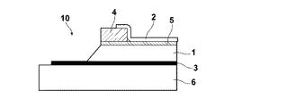
【解決手段】電圧が印加される電圧印加電極2と、放射線の照射を受けることにより電荷を発生する光導電層1と、放射線の量に対応した電荷を収集する電荷収集電極3とが積層された放射線画像検出器10において、電圧印加電極2と光導電層1との間に、電圧印加電極と同極性の電荷はブロックするが、異極性の電荷は輸送する選択的電荷輸送層4を設け、この選択的電荷輸送層4が電圧印加電極2の端部において厚膜に形成されているものとする。
【選択図】図1
Description

以下に本発明の放射線検出器の実施例を示す。
電荷収集電極、蓄積容量、TFTスイッチを有する画素構造、TFTスイッチをON・OFFする走査配線、電荷が読み出されるデータ配線が配列されたアクティブマトリクス基板上に、Seから成る光導電層を蒸着により200μmの厚みで形成した。次いで画像欠陥の発生を防止する為の硫化アンチモン(Sb2S3)層を真空蒸着により0.3μm厚で設置した。
実施例1において、ホール輸送性材料Aを含まないポリカーボネート樹脂溶液のみを用いて同じ厚み、幅で厚膜部を設け、さらにこの厚膜部の上にシリコン樹脂からなる絶縁性層を100μm厚で設けた以外は、実施例1と同様にして放射線検出器を製造した。
比較例1において、厚膜部も絶縁性層も設けなかった以外は同様にして放射線検出器を製造した。
読み取り電極ラインを配したガラス基板上にSeからなる読取用光導電層を蒸着により15μmの厚みで形成し、その上に、As2Se3から成る電子蓄積層を1.0μm厚、Seからなる記録用光導電層を200μm厚で、順次、蒸着により製膜した。この上にインクジェット装置を用いてトリクロロエチレンに溶解したポリビニルカルバゾールを0.4μmの厚みで金電極のエッジに相当する位置(Se層の端部)に3mmの幅でスリット状に塗布した(厚膜部)。設けた厚膜部の中央にエッジ部が位置するように金を蒸着し、電圧印加電極を形成し、光読取方式の放射線検出器を製造した。光読取方式における上記以外の構成については、特開2000-105297号公報の記載に従って作製した。
実施例2において、ポリビニルカルバゾールからなる厚膜部を設けることなく、絶縁体であるポリカーボネートを1μm厚みで設置した以外は、実施例2と同様にして放射線検出器を製造した。
比較例3において、絶縁性層を設けなかった以外は同様にして放射線検出器を製造した。
実施例1、2および比較例1〜4の放射線検出器を耐久性試験装置にセットし、実施例1、比較例1および2の放射線検出器については、バイアス電極に6kVの負バイアスを、実施例2、比較例3および4の放射線検出器については、バイアス電極に2kVの負バイアス矩形波で印加を繰り返し、放電破壊に至るまで印加を継続した。結果を表1に示す。
2 電圧印加電極
3 電荷収集電極
4 選択的電荷輸送層
5 電荷輸送層
6 基板
10 放射線検出器
Claims (4)
- 電圧が印加される電圧印加電極と、放射線の照射を受けることにより電荷を発生する光導電層と、放射線の量に対応した電荷を収集する電荷収集電極とが積層された放射線画像検出器において、
前記電圧印加電極と前記光導電層との間に、前記電圧印加電極と同極性の電荷はブロックするが、異極性の電荷は輸送する選択的電荷輸送層を設け、該選択的電荷輸送層が前記電圧印加電極の端部において厚膜に形成されていることを特徴とする放射線検出器。 - 電圧が印加される電圧印加電極と、放射線の照射を受けることにより電荷を発生する光導電層と、放射線の量に対応した電荷を収集する電荷収集電極とが積層された放射線画像検出器において、
前記電圧印加電極の端部と前記光導電層との間のみに、前記電圧印加電極と同極性の電荷はブロックするが、異極性の電荷は輸送する選択的電荷輸送層を設けたことを特徴とする放射線検出器。 - 前記選択的電荷輸送層が、無機の選択性輸送性材料層と有機の選択性輸送材料層との積層構造からなることを特徴とする請求項1または2記載の放射線検出器。
- 前記電圧印加電極が負バイアスであって、前記選択的電荷輸送層が、少なくともトリフェニルアミン誘導体を含む層またはポリビニルカルバゾールを含む層であることを特徴とする請求項1、2または3記載の放射線検出器。
Priority Applications (2)
| Application Number | Priority Date | Filing Date | Title |
|---|---|---|---|
| JP2007254584A JP2009088154A (ja) | 2007-09-28 | 2007-09-28 | 放射線検出器 |
| US12/240,358 US8022451B2 (en) | 2007-09-28 | 2008-09-29 | Radiation detector |
Applications Claiming Priority (1)
| Application Number | Priority Date | Filing Date | Title |
|---|---|---|---|
| JP2007254584A JP2009088154A (ja) | 2007-09-28 | 2007-09-28 | 放射線検出器 |
Publications (1)
| Publication Number | Publication Date |
|---|---|
| JP2009088154A true JP2009088154A (ja) | 2009-04-23 |
Family
ID=40661210
Family Applications (1)
| Application Number | Title | Priority Date | Filing Date |
|---|---|---|---|
| JP2007254584A Pending JP2009088154A (ja) | 2007-09-28 | 2007-09-28 | 放射線検出器 |
Country Status (2)
| Country | Link |
|---|---|
| US (1) | US8022451B2 (ja) |
| JP (1) | JP2009088154A (ja) |
Cited By (1)
| Publication number | Priority date | Publication date | Assignee | Title |
|---|---|---|---|---|
| JP2011096914A (ja) * | 2009-10-30 | 2011-05-12 | Mitsubishi Chemicals Corp | 太陽電池及びその製造方法 |
Families Citing this family (8)
| Publication number | Priority date | Publication date | Assignee | Title |
|---|---|---|---|---|
| US8629423B1 (en) * | 2008-09-19 | 2014-01-14 | Nikolai Kislov | Non-planar metal-insulator-metal tunneling device for sensing and/or generation of electromagnetic radiation at terahertz, infrared, and optical frequencies and technology of its preparation |
| US8742531B2 (en) * | 2008-12-08 | 2014-06-03 | Arizona Board Of Regents, Acting For And On Behalf Of Arizona State University | Electrical devices including dendritic metal electrodes |
| US8384041B2 (en) * | 2010-07-21 | 2013-02-26 | Carestream Health, Inc. | Digital radiographic imaging arrays with reduced noise |
| US8765514B1 (en) * | 2010-11-12 | 2014-07-01 | L-3 Communications Corp. | Transitioned film growth for conductive semiconductor materials |
| CN104823280B (zh) * | 2012-12-10 | 2018-04-03 | 富士胶片株式会社 | 放射线检测装置 |
| US11016202B2 (en) | 2018-04-26 | 2021-05-25 | Varian Medical Systems, Inc. | Imaging devices |
| US10444378B1 (en) * | 2018-04-27 | 2019-10-15 | Varian Medical Systems, Inc. | Imaging devices |
| WO2019210247A1 (en) * | 2018-04-26 | 2019-10-31 | Varian Medical Systems, Inc. | Imaging devices |
Citations (4)
| Publication number | Priority date | Publication date | Assignee | Title |
|---|---|---|---|---|
| JPH06260664A (ja) * | 1993-03-05 | 1994-09-16 | Dainippon Printing Co Ltd | 光センサーの製造方法 |
| JPH0982932A (ja) * | 1995-09-20 | 1997-03-28 | Hitachi Ltd | 固体撮像素子 |
| JP2003133575A (ja) * | 2001-10-22 | 2003-05-09 | Shimadzu Corp | 放射線検出装置 |
| JP2007150277A (ja) * | 2005-11-01 | 2007-06-14 | Fujifilm Corp | 放射線撮像パネルを構成する光導電層および放射線撮像パネル |
Family Cites Families (2)
| Publication number | Priority date | Publication date | Assignee | Title |
|---|---|---|---|---|
| EP0898421A3 (en) * | 1997-08-19 | 2001-12-05 | Fuji Photo Film Co., Ltd. | Electrostatic recording member, electrostatic latent image recording apparatus, and electrostatic latent image read-out apparatus |
| JP3678162B2 (ja) * | 2001-04-12 | 2005-08-03 | 株式会社島津製作所 | 放射線検出装置 |
-
2007
- 2007-09-28 JP JP2007254584A patent/JP2009088154A/ja active Pending
-
2008
- 2008-09-29 US US12/240,358 patent/US8022451B2/en not_active Expired - Fee Related
Patent Citations (4)
| Publication number | Priority date | Publication date | Assignee | Title |
|---|---|---|---|---|
| JPH06260664A (ja) * | 1993-03-05 | 1994-09-16 | Dainippon Printing Co Ltd | 光センサーの製造方法 |
| JPH0982932A (ja) * | 1995-09-20 | 1997-03-28 | Hitachi Ltd | 固体撮像素子 |
| JP2003133575A (ja) * | 2001-10-22 | 2003-05-09 | Shimadzu Corp | 放射線検出装置 |
| JP2007150277A (ja) * | 2005-11-01 | 2007-06-14 | Fujifilm Corp | 放射線撮像パネルを構成する光導電層および放射線撮像パネル |
Cited By (1)
| Publication number | Priority date | Publication date | Assignee | Title |
|---|---|---|---|---|
| JP2011096914A (ja) * | 2009-10-30 | 2011-05-12 | Mitsubishi Chemicals Corp | 太陽電池及びその製造方法 |
Also Published As
| Publication number | Publication date |
|---|---|
| US20090250619A1 (en) | 2009-10-08 |
| US8022451B2 (en) | 2011-09-20 |
Similar Documents
| Publication | Publication Date | Title |
|---|---|---|
| JP5213378B2 (ja) | 放射線検出器 | |
| JP2009088154A (ja) | 放射線検出器 | |
| US7786446B2 (en) | Radiation detector | |
| JP4907418B2 (ja) | 放射線画像検出器 | |
| JP5230791B2 (ja) | 放射線検出器 | |
| US7728299B2 (en) | Radiation image detector | |
| JP2008256677A (ja) | 放射線画像検出器 | |
| JP2009212162A (ja) | 放射線検出器 | |
| JP5070031B2 (ja) | 放射線画像検出器 | |
| JP5070130B2 (ja) | 放射線検出器 | |
| JP4940125B2 (ja) | 放射線検出器 | |
| JP2012154933A (ja) | 放射線検出器 | |
| JP2009088200A (ja) | 放射線検出器 | |
| JP2009036570A (ja) | 放射線検出器 | |
| JP5235119B2 (ja) | 放射線画像検出器 | |
| JP2004186604A (ja) | 画像記録媒体 | |
| JP4990084B2 (ja) | 放射線検出器 | |
| JP5270121B2 (ja) | 画像撮像装置 | |
| JP2010098102A (ja) | 放射線画像検出器 | |
| JP5207451B2 (ja) | 放射線画像検出器 | |
| JP5077921B2 (ja) | 放射線固体センサーおよびその製造方法 | |
| JP2009054923A (ja) | 放射線画像検出器の製造方法 | |
| JP2007150278A (ja) | 放射線撮像パネルを構成する光導電層および放射線撮像パネル | |
| JP2009135245A (ja) | 放射線画像検出器 |
Legal Events
| Date | Code | Title | Description |
|---|---|---|---|
| A621 | Written request for application examination |
Free format text: JAPANESE INTERMEDIATE CODE: A621 Effective date: 20100226 |
|
| RD15 | Notification of revocation of power of sub attorney |
Free format text: JAPANESE INTERMEDIATE CODE: A7435 Effective date: 20110427 |
|
| A131 | Notification of reasons for refusal |
Free format text: JAPANESE INTERMEDIATE CODE: A131 Effective date: 20111004 |
|
| A977 | Report on retrieval |
Free format text: JAPANESE INTERMEDIATE CODE: A971007 Effective date: 20111005 |
|
| A02 | Decision of refusal |
Free format text: JAPANESE INTERMEDIATE CODE: A02 Effective date: 20120410 |