JP2009092995A - Electro-optic element and light beam deflector - Google Patents
Electro-optic element and light beam deflector Download PDFInfo
- Publication number
- JP2009092995A JP2009092995A JP2007264426A JP2007264426A JP2009092995A JP 2009092995 A JP2009092995 A JP 2009092995A JP 2007264426 A JP2007264426 A JP 2007264426A JP 2007264426 A JP2007264426 A JP 2007264426A JP 2009092995 A JP2009092995 A JP 2009092995A
- Authority
- JP
- Japan
- Prior art keywords
- electro
- optic
- refractive index
- crystal
- voltage
- Prior art date
- Legal status (The legal status is an assumption and is not a legal conclusion. Google has not performed a legal analysis and makes no representation as to the accuracy of the status listed.)
- Granted
Links
Images


Landscapes
- Optical Modulation, Optical Deflection, Nonlinear Optics, Optical Demodulation, Optical Logic Elements (AREA)
Abstract
Description
本発明は、電気光学結晶材料を用いた電気光学素子及び光ビーム偏向器に係り、特にレーザプリンタ、レーザ走査顕微鏡、バーコードリーダー等のスキャナー部、光通信用スイッチ素子に用いられる電気光学素子及び光ビーム偏向器に関する。 The present invention relates to an electro-optic element and an optical beam deflector using an electro-optic crystal material, and more particularly to a scanner unit such as a laser printer, a laser scanning microscope, and a barcode reader, an electro-optic element used for an optical communication switch element, and The present invention relates to a light beam deflector.
入力信号に応じて光ビームを任意の角度に走査することが可能な電気光学素子は、様々な用途、例えばレーザプリンタ、プロジェクタおよびディスプレイ等の映像機器、光通信、光記録、光造形、各種センシングデバイス等を構成する際の基本素子である。 Electro-optical elements that can scan a light beam at an arbitrary angle according to an input signal are used in various applications, for example, video equipment such as laser printers, projectors, and displays, optical communication, optical recording, optical modeling, and various types of sensing. It is a basic element for configuring devices and the like.
電気光学素子に求められる性能として、広角に走査可能であること、高速に走査可能であること、低消費電力あるいは低電圧の入力信号で動作可能であること、小型であること、耐衝撃性に優れること等が挙げられる。
これまでに様々な電気光学素子が提案されているが、上記の要求を全て満足させることはできていない。
以下に現在電気光学素子として用いられている代表的な従来技術を述べる。
The performance required for electro-optic elements is that it can be scanned at a wide angle, that it can be scanned at high speed, that it can operate with low power consumption or low-voltage input signals, that it is compact, and that it is shock resistant. It is excellent.
Various electro-optic elements have been proposed so far, but all of the above requirements cannot be satisfied.
The typical prior art currently used as an electro-optical element will be described below.
光ビームを広角に走査可能な光偏向技術として、ポリゴンミラーやガルバノミラーを機械的に駆動する方法がある。
しかしながら、ミラーをモータ駆動により駆動させるため、動作速度が最大でも数百Hzと遅く、素子の小型化が困難であり、消費電力も大きいといった問題がある。
また、MEMS(Micro Electro Mechanical Systems)技術により形成されたミラーを用いると、素子の小型化および複数の素子の集積化は可能となるが、MHz以上の高速な駆動は困難であり、また機械的な強度に対する信頼性が低い。
As a light deflection technique capable of scanning a light beam at a wide angle, there is a method of mechanically driving a polygon mirror or a galvanometer mirror.
However, since the mirror is driven by motor driving, the operation speed is as slow as several hundred Hz at the maximum, and it is difficult to reduce the size of the element and power consumption is high.
In addition, if a mirror formed by MEMS (Micro Electro Mechanical Systems) technology is used, it is possible to reduce the size of the element and integrate a plurality of elements, but it is difficult to drive at a high speed of MHz or more, and mechanically. Low reliability for strong strength.
機械的な駆動部を持たない方式として、音響光学効果(AO(Acousto-Optic )効果)を利用した光偏向素子がある。AO偏向器は数百kHz程度の比較的高速で動作し、また高い音響周波数により大きな偏向角を得ることができる。
しかしながら、AO偏向器は超音波発生部分を持つため、素子の小型化は困難であり、さらに数百MHzの弾性波励起信号を必要とするために駆動システムが複雑でかつ大きくなることが避けられない。
As a method without a mechanical drive unit, there is an optical deflection element using an acousto-optic effect (AO (Acousto-Optic) effect). The AO deflector operates at a relatively high speed of about several hundred kHz, and can obtain a large deflection angle with a high acoustic frequency.
However, since the AO deflector has an ultrasonic wave generation part, it is difficult to reduce the size of the element. Further, since the AO deflector requires an elastic wave excitation signal of several hundred MHz, the drive system cannot be complicated and large. Absent.
また高速に光ビームを走査することが可能な技術として、電気光学効果(EO(Electro- Optic)効果)による光学材料の屈折率変化を利用した光偏向素子がある。例えばニオブ酸リチウム(LiNbO3:LN)やタンタル酸リチウム(LiTaO3:LT)等の電気光学結晶基板表面にプリズム形状の電極を形成、あるいは電気光学結晶にプリズム形状などの分極反転領域をパターニングし、電圧を印加することによって屈折率変化を起こすことでビームを偏向させる。
例えば特許文献1では、この原理を利用し、プリズム状電極を複数設けたマルチビーム対応の光スイッチ素子を報告している。
しかしながら、一般的に電気光学効果による屈折率変化量は極めて小さいため、大きな偏向角を得るためには素子のサイズも大きくする必要があり、さらには駆動電圧も大きくする必要がある。
Further, as a technique capable of scanning a light beam at high speed, there is an optical deflection element that uses a change in refractive index of an optical material due to an electro-optic effect (EO (Electro-Optic) effect). For example, a prism-shaped electrode is formed on the surface of an electro-optic crystal substrate such as lithium niobate (LiNbO 3 : LN) or lithium tantalate (LiTaO 3 : LT), or a polarization inversion region such as a prism shape is patterned on the electro-optic crystal. The beam is deflected by causing a refractive index change by applying a voltage.
For example,
However, since the amount of change in the refractive index due to the electro-optic effect is generally very small, it is necessary to increase the element size and to increase the driving voltage in order to obtain a large deflection angle.
以上の光偏向技術の他に、非特許文献1において、空間電荷制御電気伝導を利用したビーム偏向素子が報告されている。これは電気光学結晶への電子注入により、電気光学効果による屈折率変化に傾斜が生じ、広角な光偏向が生じる現象である。非特許文献1では、大きなEO効果を有するKTN結晶基板の上下面に金属電極を成膜し、電圧を印加することにより、基板の膜厚方向に全角10°程度の大きなビーム偏向を実現している。
以下にこの空間電荷制御電気伝導を利用したビーム偏向素子の動作原理を図22(a)〜(c)を参照して説明する。
In addition to the above optical deflection technique, Non-Patent
The operation principle of the beam deflection element using the space charge controlled electric conduction will be described below with reference to FIGS. 22 (a) to 22 (c).
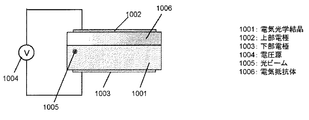
図22(a)は従来の電気光学素子を横から見た様子を表す図であり、電気光学素子は電気光学結晶からなる基板の両面(図では上下の面)に電極となる金属薄膜を形成して構成される。
ここで、電極と結晶との接触をオーミック接触とすると、結晶内部に電子が注入される。空間電荷効果とは、結晶内部に注入された電子によって陽極から発する電界が終端される効果であり。この効果によって電極間の電界が不均一になる。光学結晶内部に電子が注入されたときの電界分布は式(1)で与えられる。
FIG. 22A is a diagram showing a conventional electro-optic element viewed from the side. The electro-optic element is formed by forming a metal thin film as an electrode on both surfaces (upper and lower faces in the figure) of a substrate made of an electro-optic crystal. Configured.
Here, when the contact between the electrode and the crystal is ohmic contact, electrons are injected into the crystal. The space charge effect is an effect in which the electric field emitted from the anode is terminated by electrons injected into the crystal. This effect makes the electric field between the electrodes non-uniform. The electric field distribution when electrons are injected into the optical crystal is given by equation (1).
ここでVは印加電圧を表し、dは結晶の厚さを表し、xは結晶の厚さ方向の座標を表す(0≦x≦d)。したがって、図22(a)に示した電気光学結晶内の電界分布は図22(b)に示すように、結晶の厚さ方向に異なる値をもつ。電気光学結晶がカー効果による屈折率変化を示す場合、結晶内部に電界が形成されたときの結晶の屈折率変化量Δnは式(2)で与えられる。 Here, V represents an applied voltage, d represents the thickness of the crystal, and x represents coordinates in the thickness direction of the crystal (0 ≦ x ≦ d). Therefore, the electric field distribution in the electro-optic crystal shown in FIG. 22A has different values in the thickness direction of the crystal as shown in FIG. When the electro-optic crystal exhibits a refractive index change due to the Kerr effect, the refractive index change amount Δn of the crystal when an electric field is formed inside the crystal is given by equation (2).
n0は結晶の屈折率であり、sijはカー定数である。式(1)および式(2)より、空間電荷効果によって生じる電気光学結晶内の屈折率変化量は図22(c)に示すような分布を持つ。すなわち、正の電圧を印加した電極付近が最も屈折率が低く、反対の電極付近の屈折率が最も高い。電圧を印加された結晶材料がカー効果によって屈折率変化する場合、結晶の厚さ方向で屈折率は線形に変化する。
ここで結晶の断面から光ビームを入力すると、光は屈折率の高い方向へ偏向しながら伝搬する。相互作用長、すなわち屈折率分布をもつ結晶内を伝搬する長さをLとすると、結晶内部での偏向角θiは次式(3)で与えられる。
n 0 is the refractive index of the crystal and s ij is the Kerr constant. From the equations (1) and (2), the refractive index change amount in the electro-optic crystal caused by the space charge effect has a distribution as shown in FIG. That is, the refractive index is the lowest near the electrode to which a positive voltage is applied, and the refractive index is the highest near the opposite electrode. When the refractive index of a crystal material to which a voltage is applied changes due to the Kerr effect, the refractive index changes linearly in the thickness direction of the crystal.
Here, when a light beam is inputted from the cross section of the crystal, the light propagates while being deflected in a direction having a high refractive index. When the interaction length, that is, the length of propagation in the crystal having a refractive index distribution is L, the deflection angle θi inside the crystal is given by the following equation (3).
さらに結晶から出射するときの偏向角θは偏向角が小さい場合にはスネルの法則より、式(4)で与えられる。 Further, when the deflection angle is small, the deflection angle θ when emitted from the crystal is given by the equation (4) from Snell's law.
以上の原理から具体的に結晶内部における屈折率分布および、ビーム偏向角を計算した例を示す。
ここでは結晶の屈折率をn0=2.2とし、カー定数をsij=1.0×10⁻¹⁴m2/V2とし、結晶厚をd=500μmとし、相互作用長をL=5mmとした。
Here, the refractive index of the crystal is n 0 = 2.2, the Kerr constant is s ij = 1.0 × 10 −14 m 2 / V 2 , the crystal thickness is d = 500 μm, and the interaction length is L = 5 mm. It was.
ここで、電圧印加によって生じる結晶内の屈折率変化の分布を図23に示す。図23において横軸は屈折率差を示し、縦軸は変位を示す。
正の電圧印加によって負の屈折率変化が生じ、逆に負の電圧印加によって正の屈折率変化が生じる。また印加電圧を大きくすることにより、結晶内部の屈折変化量も増大する。
図24(a)は電気光学素子の断面を示し、図24(b)は図24(a)に示した電気光学素子の印加電圧に対する出射ビームの偏向角およびビーム偏向に伴う膜厚方向のビーム位置の変移量、すなわち光ビームの入射位置と出射位置の膜厚方向の差を示している。図24(b)において横軸は印加電圧を示し、左縦軸は偏向角度を示し、右縦軸は変位量を示す。
偏向角度は印加電圧の2乗に比例して増大し、理論的には±200Vの電圧印加により±10°以上のビーム偏向が可能になる。ただし光ビームを結晶の厚さ方向の中央から入射した場合、ビーム偏向に伴うビーム位置の変移量は、結晶厚の1/2以下、すなわちこの例では250μm以下であることが必要である。変移量が250μm以上になると、結晶内部を伝搬した光が出射端面に至るより前に結晶の上下面において光ビームが反射してしまう。
結晶に印加可能な電圧量はこのビーム位置の変移量によって制限され、この例では±200V程度以下で素子を動作させることが必要になる。
Here, the distribution of the refractive index change in the crystal caused by the voltage application is shown in FIG. In FIG. 23, the horizontal axis indicates the refractive index difference, and the vertical axis indicates the displacement.
A negative refractive index change occurs when a positive voltage is applied, and a positive refractive index change occurs when a negative voltage is applied. Further, by increasing the applied voltage, the amount of change in refraction inside the crystal also increases.
24A shows a cross section of the electro-optic element, and FIG. 24B shows the deflection angle of the emitted beam with respect to the applied voltage of the electro-optic element shown in FIG. 24A and the beam in the film thickness direction accompanying the beam deflection. The position shift amount, that is, the difference between the incident position and the exit position of the light beam in the film thickness direction is shown. In FIG. 24B, the horizontal axis represents the applied voltage, the left vertical axis represents the deflection angle, and the right vertical axis represents the displacement amount.
The deflection angle increases in proportion to the square of the applied voltage. Theoretically, a beam deflection of ± 10 ° or more becomes possible by applying a voltage of ± 200V. However, when the light beam is incident from the center in the thickness direction of the crystal, the shift amount of the beam position accompanying the beam deflection needs to be 1/2 or less of the crystal thickness, that is, 250 μm or less in this example. When the amount of displacement is 250 μm or more, the light beam is reflected on the upper and lower surfaces of the crystal before the light propagated inside the crystal reaches the emission end face.
The amount of voltage that can be applied to the crystal is limited by the amount of shift of the beam position. In this example, it is necessary to operate the device at about ± 200 V or less.
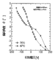
非特許文献1では、電気光学結晶としてKTN(KTal-xNbxO3)結晶を用い、オーミック接触を達成するために電極材料としてTiを採用している。さらに動作温度をキュリー温度に近づけることで大きな偏向角を得ている。また上記の空間電荷効果によるビーム偏向はKTN特有の現象ではなく、大きな電気光学効果を有する材料であれば同様のビーム偏向が可能である。例えばニオブ酸ストロンチウムバリウム(SrxBa1-xNbO3:SBN)結晶等は高い電気光学係数を持ち、空間電荷効果を利用した光偏向を構成するための電気光学材料として好適である。
図25はSBN(x=61)にTi電極を形成して電圧を印加し、ビーム偏向角を測定した結果である。同図において横軸は印加電圧を示し、縦軸は偏向角度を示す。
ここで結晶の厚さをd=500μmとし、相互作用長をL=7mmとした。また動作温度75℃および87℃としてそれぞれ印加電圧とビーム偏向角の関係をプロットした。
SBN(x=61)はキュリー温度が80℃であり、動作温度がキュリー温度以下の場合、電気光学結晶はポッケルス効果によってその屈折率が変化する。このとき、結晶内の電界量と屈折率変化量との間には式(5)の関係がある。
FIG. 25 shows the result of measuring the beam deflection angle by forming a Ti electrode on SBN (x = 61) and applying a voltage. In the figure, the horizontal axis indicates the applied voltage, and the vertical axis indicates the deflection angle.
Here, the thickness of the crystal was d = 500 μm, and the interaction length was L = 7 mm. Further, the relationship between the applied voltage and the beam deflection angle was plotted at operating temperatures of 75 ° C. and 87 ° C., respectively.
SBN (x = 61) has a Curie temperature of 80 ° C., and when the operating temperature is equal to or lower than the Curie temperature, the refractive index of the electro-optic crystal changes due to the Pockels effect. At this time, there is a relationship of the formula (5) between the electric field amount in the crystal and the refractive index change amount.
ここでrijはポッケルス係数である。また、ポッケルス効果と空間電荷効果とを組み合わせた場合、電圧印加量に対してビーム偏向角はほぼ線形に変化することが理論的に導かれるが、図25に示したように75℃で動作させた場合の実験結果も印加電圧が±50V以下程度の範囲では印加電圧に対してビーム偏向角は線形に変化している。
またキュリー温度以上の動作温度ではビーム偏向角は電圧印加量の2乗に比例するが、キュリー温度以上である87℃で動作させた場合の測定結果もビーム偏向角は電圧印加量の2乗にほぼ比例していることがわかる。また、いずれの動作温度についてもキュリー温度に近い温度で動作させたため、±4°以上の大きなビーム偏向角が得られた。
Here, r ij is a Pockels coefficient. In addition, when the Pockels effect and the space charge effect are combined, it is theoretically derived that the beam deflection angle changes almost linearly with respect to the applied voltage, but it is operated at 75 ° C. as shown in FIG. In the experimental results, the beam deflection angle changes linearly with respect to the applied voltage in the range where the applied voltage is about ± 50 V or less.
The beam deflection angle is proportional to the square of the voltage application amount at an operating temperature equal to or higher than the Curie temperature, but the measurement result when operating at 87 ° C., which is equal to or higher than the Curie temperature, also indicates that the beam deflection angle is the square of the voltage application amount. It turns out that it is almost proportional. Further, since any operating temperature was operated at a temperature close to the Curie temperature, a large beam deflection angle of ± 4 ° or more was obtained.
空間電荷制御電気伝導を利用したビーム偏向素子は、機械的な駆動部を持たないため、ミラー駆動型およびMEMS(Micro Electro Mechanical System)型と比較すると耐衝撃性に優れ、高速動作が可能である。また固体光学結晶基板に電圧を印加するのみで動作可能であるため、AO偏向器と比較して駆動システムを簡素化でき、さらにデバイス長が数mm程度と小型であるにも係らず、偏向角を10°程度まで大きくできるといった特徴を有する。 The beam deflection element using space charge controlled electrical conduction does not have a mechanical drive, so it is superior in impact resistance compared to the mirror drive type and MEMS (Micro Electro Mechanical System) type, and can operate at high speed. . In addition, since it can be operated simply by applying a voltage to the solid optical crystal substrate, the drive system can be simplified compared to an AO deflector, and the deflection angle is small despite the device length being only a few millimeters. It can be increased to about 10 °.
ただし、空間電荷制御電気伝導を利用したビーム偏向素子を駆動するためには数100V程度の高電圧の印加を必要とする。理論的には駆動電圧は式(1)から分かるように電気光学結晶の厚さを薄くすることで低減できる。例として結晶の厚さを100μmとしたときの電圧印加量とビーム偏向角の関係を見積もってみる。
ここではカー効果と空間電荷とを組み合わせてビーム偏向が発生する場合を考え、結晶の屈折率をn0=2.2とし、カー定数をsij=1.0×10⁻¹⁴m2/V2とし、結晶厚をd=100μmとし、相互作用長をL=5mmと仮定する。
However, in order to drive the beam deflection element using space charge controlled electrical conduction, it is necessary to apply a high voltage of about several hundred volts. Theoretically, the drive voltage can be reduced by reducing the thickness of the electro-optic crystal, as can be seen from equation (1). As an example, the relationship between the voltage application amount and the beam deflection angle when the crystal thickness is 100 μm is estimated.
Here, considering the case where beam deflection occurs by combining the Kerr effect and space charge, the refractive index of the crystal is n 0 = 2.2, and the Kerr constant is s ij = 1.0 × 10 −14 m 2 / V. 2 is assumed, the crystal thickness is d = 100 μm, and the interaction length is L = 5 mm.
図26に上記パラメータにおける印加電圧と偏向角およびビーム偏向に伴う膜厚方向のビーム位置の変移量との関係を示す。同図において、横軸は印加電圧を示し、縦軸は偏向角度を示す。
結晶の厚さが500μmである図24の場合と比較して、8V程度の低電圧で±2°程度の偏向角が得られる。ただし、電圧印加量が8Vを超えると、ビームの出射位置が膜厚方向に50μm以上すなわち結晶厚さの1/2以上移動してしまう。したがって8V以上の電圧印加時は、出射端面に至るより前に結晶の上下面において光ビームが反射してしまう。結果的として、結晶の厚さを薄くすることによって、低電圧での駆動は可能になるが、結晶厚方向にビームの移動が生じるという理由により偏向角を大きなビーム偏向素子の実現が困難となる。
FIG. 26 shows the relationship between the applied voltage, the deflection angle, and the shift amount of the beam position in the film thickness direction accompanying the beam deflection in the above parameters. In the figure, the horizontal axis indicates the applied voltage, and the vertical axis indicates the deflection angle.
Compared with the case of FIG. 24 in which the thickness of the crystal is 500 μm, a deflection angle of about ± 2 ° is obtained at a low voltage of about 8V. However, when the voltage application amount exceeds 8 V, the beam emission position moves in the film thickness direction by 50 μm or more, that is, ½ or more of the crystal thickness. Therefore, when a voltage of 8 V or more is applied, the light beam is reflected on the upper and lower surfaces of the crystal before reaching the emission end face. As a result, it is possible to drive at a low voltage by reducing the thickness of the crystal, but it is difficult to realize a beam deflecting element having a large deflection angle because the beam moves in the crystal thickness direction. .
上述のように、空間電荷制御電気伝導を利用したビーム偏向素子において、低電圧駆動と広角でのビーム走査との両立を可能にすることは困難であった。 As described above, it has been difficult to achieve both low-voltage driving and wide-angle beam scanning in a beam deflection element using space charge controlled electrical conduction.
本発明では、これらの問題点を解決するためのものであり、低電圧で駆動可能でありかつ、広角に光ビームを走査できる小型の電気光学素子及び光ビーム偏向器を提供することを目的とする。 An object of the present invention is to solve these problems and to provide a small electro-optic element and a light beam deflector that can be driven at a low voltage and can scan a light beam at a wide angle. To do.
上記課題を解決するため、本発明の請求項1に記載の発明は、電気光学材料からなる基板と、該基板の両面に電極領域を形成し、該各電極領域間の電気光学材料中を光が伝搬する電気光学素子において、前記光伝搬領域の屈折率が可変であることを特徴とする。
In order to solve the above-mentioned problems, the invention according to
請求項2に記載の発明は、請求項1に記載の電気光学素子において、電気光学結晶の板厚を変える前記屈折率が可変である構造は、前記基板の板厚を変えてなる構造であることを特徴とする。 According to a second aspect of the present invention, in the electro-optical element according to the first aspect, the structure in which the refractive index that changes the thickness of the electro-optic crystal is variable is a structure in which the thickness of the substrate is changed. It is characterized by that.
請求項3に記載の発明は、請求項2に記載の電気光学素子において、前記基板の板厚の変化率が漸次変化することを特徴とする。 According to a third aspect of the present invention, in the electro-optic element according to the second aspect, the change rate of the thickness of the substrate gradually changes.
請求項4に記載の発明は、請求項2に記載の電気光学素子において、前記基板の板厚が階段状に変化することを特徴とする。 According to a fourth aspect of the present invention, in the electro-optical element according to the second aspect, the thickness of the substrate changes stepwise.
請求項5に記載の発明は、請求項1から4のいずれか1項に記載の電気光学素子において、前記屈折率が可変である構造は、前記基板の密度を変えてなる構造であることを特徴とする。 According to a fifth aspect of the present invention, in the electro-optical element according to any one of the first to fourth aspects, the structure in which the refractive index is variable is a structure in which the density of the substrate is changed. Features.
請求項6に記載の発明は、請求項1から5のいずれか1項に記載の電気光学素子において、前記屈折率が可変である構造は、前記基板の分極反転領域の密度を変えてなる構造であることを特徴とする。 According to a sixth aspect of the present invention, in the electro-optic element according to any one of the first to fifth aspects, the structure in which the refractive index is variable is a structure in which the density of the domain-inverted region of the substrate is changed. It is characterized by being.
請求項7に記載の発明は、請求項1から6のいずれか1項に記載の電気光学素子において、前記屈折率が可変である構造は、前記電極領域の電気抵抗を変えてなる構造であることを特徴とする。 According to a seventh aspect of the present invention, in the electro-optic element according to any one of the first to sixth aspects, the structure in which the refractive index is variable is a structure in which the electric resistance of the electrode region is changed. It is characterized by that.
請求項8に記載の発明は、請求項1から7のいずれか1項に記載の電気光学素子において、前記電極領域が微小穴を有し、該微小穴の面密度が漸次変化することを特徴とする。 According to an eighth aspect of the present invention, in the electro-optic element according to any one of the first to seventh aspects, the electrode region has minute holes, and the surface density of the minute holes gradually changes. And
請求項9に記載の発明は、請求項1から7のいずれか1項に記載の電気光学素子において、前記電極領域が複数のストライプ形状の集合体から成り、該ストライプ形状の線幅が漸次変化することを特徴とする。 According to a ninth aspect of the present invention, in the electro-optic element according to any one of the first to seventh aspects, the electrode region comprises a plurality of stripe-shaped aggregates, and the line width of the stripe shape gradually changes. It is characterized by doing.
請求項10に記載の発明は、請求項8または9に記載の電気光学素子において、前記電極領域が少なくとも2種類の導電性材料からなり、前記導電性材料の仕事関数が互いに異なることを特徴とする。 According to a tenth aspect of the present invention, in the electro-optical element according to the eighth or ninth aspect, the electrode region is made of at least two kinds of conductive materials, and the work functions of the conductive materials are different from each other. To do.
請求項11に記載の発明は、請求項7に記載の電気光学素子において、前記電極領域が導電性材料と電気抵抗体材料との積層構造からなることを特徴とする。 According to an eleventh aspect of the present invention, in the electro-optic element according to the seventh aspect, the electrode region has a laminated structure of a conductive material and an electric resistor material.
請求項12に記載の発明は、請求項11に記載の電気光学素子において、前記電気抵抗体材料の厚さが漸次変化することを特徴とする。 According to a twelfth aspect of the present invention, in the electro-optic element according to the eleventh aspect, the thickness of the electric resistor material gradually changes.
請求項13に記載の発明は、請求項11に記載の電気光学素子において、前記電気抵抗体材料の厚さが階段状に変化することを特徴とする。 According to a thirteenth aspect of the present invention, in the electro-optic element according to the eleventh aspect, the thickness of the electric resistor material changes stepwise.
請求項14に記載の発明は、請求項1から13のいずれか1項記載の電気光学素子を用いた光ビーム偏向器であることを特徴とする。 A fourteenth aspect of the present invention is a light beam deflector using the electro-optic element according to any one of the first to thirteenth aspects.
本発明によれば、電気光学効果をもつ光学材料基板の両面から電圧を印加することによって動作し、電気光学効果と空間電界効果との組み合わせにより光偏向が可能となる。結晶内部に発生する屈折率変化の分布を制御することにより基板幅方向に光ビームを走査させる。これにより低電圧で駆動し広角に光ビームを走査することが可能な、コンパクトな電気光学素子及び光ビーム偏向器の提供を実現できる。 According to the present invention, operation is performed by applying a voltage from both surfaces of an optical material substrate having an electro-optic effect, and light deflection is possible by a combination of the electro-optic effect and the spatial electric field effect. The light beam is scanned in the substrate width direction by controlling the distribution of the change in refractive index generated in the crystal. Accordingly, it is possible to provide a compact electro-optical element and a light beam deflector that can be driven at a low voltage and can scan a light beam at a wide angle.
以下に本発明に係る電気光学素子を用いた光偏向器の実施の形態について説明する。
〔第一の実施の形態(請求項1、2:楔型横方向偏向素子)〕
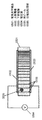
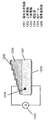
本発明の第一の実施形態を図1を用いて説明する。
図1(a)は本発明に係る電気光学素子を上面から見た図であり、図1(b)は図1(a)のIb−Ib線における電気光学素子の断面図を模式的に示した図である。
電気光学素子は電気光学結晶基板0101の両面(図1(b)の上表面および下表面)にそれぞれ上部電極0102および下部電極0103を形成して成る。また、電気光学結晶基板0101の板厚は電気光学結晶基板0101の幅方向で漸次変化させる。
すなわち電気光学結晶基板0101は楔形状となっている。
Embodiments of an optical deflector using an electro-optic element according to the present invention will be described below.
First Embodiment (
A first embodiment of the present invention will be described with reference to FIG.
FIG. 1A is a top view of an electro-optical element according to the present invention, and FIG. 1B schematically shows a cross-sectional view of the electro-optical element taken along line Ib-Ib in FIG. It is a figure.
The electro-optic element is formed by forming an
That is, the electro-
ここで電気光学結晶の電気光学定数(EO係数)が大きいほど、電気光学素子内を伝搬した後のビーム偏向角を大きくすることができる。電極材料は結晶材料との接触がオーミック接触となるように選択される。具体的には、光学結晶材料としてKIN(KTa1-xNbxO3)結晶やSBN(SrBa1-xNbO3)結晶等が好適であり、オーミック接触を実現するための電極材料としてTiやCr等が好適である。これらの電極材料はスパッタや蒸着等により結晶面上に薄膜として形成できる。
光学結晶材料を楔形状に加工することは例えば高精度な研磨加工技術等によって実現可能である。
図1(a)、(b)では上部電極0102及び下部電極0103の寸法を電気光学結晶0101よりやや小さく形成してある。これは上部電極0102―下部電極0103間に印加した電圧によって電気光学結晶0101の側面に表面電流が発生することを抑制する効果がある。
特に電気光学結晶0101の厚さが薄い時には上部電極0102と下電極0103とが短絡し易くなるため、両電極0102、0103の寸法を電気光学結晶0101より小さくしておくことが好ましい。
具体的には、それぞれ電気光学結晶0101の四方を両電極0102、0103の大きさより数百μm〜1mm程度広くすれば十分である。
Here, the larger the electro-optic constant (EO coefficient) of the electro-optic crystal, the larger the beam deflection angle after propagating in the electro-optic element. The electrode material is selected such that the contact with the crystal material is an ohmic contact. Specifically, KIN (KTa 1-x Nb x O 3 ) crystal, SBN (SrBa 1-x NbO 3 ) crystal or the like is suitable as the optical crystal material, and Ti or the like is used as the electrode material for realizing ohmic contact. Cr or the like is preferred. These electrode materials can be formed as a thin film on the crystal plane by sputtering or vapor deposition.
Processing the optical crystal material into a wedge shape can be realized by, for example, a highly accurate polishing technique.
In FIGS. 1A and 1B, the
In particular, when the electro-
Specifically, it is sufficient to make the four sides of the electro-
上部電極0102および下部電極0103の間に電圧を印加することにより、電気光学結晶0101の内部に電子が注入される。空間電荷効果と電気光学効果とが組み合わさり、電圧印加により電気光学結晶0101の屈折率が変化する。
ここで正の電圧を電気光学結晶0101に印加することで、負の屈折率変化が生じる。上部電極0102と下部電極0103との間の距離が狭いほど電気光学結晶0101の内部に形成される電界が大きくなるため屈折率変化量も大きくなる。
By applying a voltage between the
Here, applying a positive voltage to the electro-
電気光学結晶0101の厚さを図1(b)に示すように変化させ、楔型の断面形状となるようにすると、Ib−Ib線上で電気光学結晶0101の厚さが異なるから、電気光学結晶0101内に形成される屈折率変化量もIb−Ib線上で異なる。
図13(a)は図1(b)に示した電気光学素子をxy座標の第一象限に表示した図であり、図13(b)は図1(b)のVII−VII線における屈折率変化量を表した図である。図13(b)において横軸はy座標における位置を示し、縦軸は屈折率変化を示す。
ここで電気光学結晶0101の内部への電界形成によって生じる電気光学効果として2次のカー効果を想定し、カー定数sij=1.0×10⁻¹⁴m2/V2を仮定した。
When the thickness of the electro-
FIG. 13A is a diagram in which the electro-optic element shown in FIG. 1B is displayed in the first quadrant of the xy coordinates, and FIG. 13B is a refractive index along the line VII-VII in FIG. It is a figure showing the amount of change. In FIG. 13B, the horizontal axis indicates the position in the y coordinate, and the vertical axis indicates the refractive index change.
Here, a second-order Kerr effect is assumed as an electro-optic effect generated by forming an electric field inside the electro-
以降では、電気光学結晶の厚さ方向にx軸をとり、電気光学結晶の幅方向にy軸をとり、光ビームの入射光軸に平行にz軸をとって説明する。
電気光学結晶の下面での座標をx=0とし、電気光学結晶に電界が形成される左端の座標をy=0とする。電気光学結晶の厚さが最も小さいところで100μm(dmin)、最も厚いところで500μm(dmax)とした。電気光学結晶の幅をw=500μmとし、y=0〜wの範囲においてdminとdmaxとの間は線形に変化するものとした。
図13はx=80μmの線上における屈折率変化量を示したものである。電圧印加量をパラメータとして5〜20Vまで変化させた。電圧印加量を大きくするほど屈折率変化量の絶対値も大きくなり、またy座標が小さいほど電気光学結晶の厚さが相対的に小さいため、屈折率変化量の絶対値も大きくなることがわかる。
In the following description, the x-axis is taken in the thickness direction of the electro-optic crystal, the y-axis is taken in the width direction of the electro-optic crystal, and the z-axis is taken parallel to the incident optical axis of the light beam.
The coordinate on the lower surface of the electro-optic crystal is x = 0, and the leftmost coordinate at which an electric field is formed on the electro-optic crystal is y = 0. The thickness of the electro-optic crystal was the smallest at 100 μm (d min ) and the thickest at 500 μm (d max ). The width of the electro-optic crystal was w = 500 μm, and the range between d min and d max was linearly changed in the range of y = 0 to w.
FIG. 13 shows the amount of change in the refractive index on the line of x = 80 μm. The voltage application amount was varied from 5 to 20 V as a parameter. It can be seen that the absolute value of the refractive index change amount increases as the voltage application amount increases, and the thickness of the electro-optic crystal is relatively small as the y coordinate decreases, so that the absolute value of the refractive index change amount also increases. .
図13のような屈折率分布を持つ媒質に光ビームを入力することを考える。y座標が大きくなるほど、屈折率が大きくなるから、y座標が小さいすなわち、電気光学結晶0101の厚さが薄いところに光ビームを入力すると、相対的に屈折率の大きい方向(y座標が大きくなる方向)に光ビームは偏向しながら伝搬する。すなわち電気光学結晶0101の基板の幅方向に水平な方向に光ビームが偏向する。Δnがy座標に依存して変化するとき、ビームの横方向への偏向角は式(6)で与えられる。
Consider inputting a light beam into a medium having a refractive index distribution as shown in FIG. As the y coordinate increases, the refractive index increases. Therefore, when the y coordinate is small, that is, when a light beam is input to a place where the thickness of the electro-
式(6)においてLは相互作用長である。 In equation (6), L is the interaction length.
従来の空間電荷効果を利用した偏向素子においては、光ビームは電気光学結晶基板の厚さ方向に偏向するため、電気光学結晶の厚さが制限され、低電圧駆動が難しい。これに対して、上述のような横方向のビーム偏向では電気光学結晶厚さに対する制限が緩和され、低電圧駆動が可能になる。 In a conventional deflection element using the space charge effect, the light beam is deflected in the thickness direction of the electro-optic crystal substrate, so that the thickness of the electro-optic crystal is limited and low voltage driving is difficult. On the other hand, in the lateral beam deflection as described above, the restriction on the thickness of the electro-optic crystal is relaxed, and low voltage driving becomes possible.
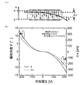
図14(a)は図1(a)に示した電気光学素子をzy座標の第一象限に表示した図であり、図14(b)は上記の構造パラメータについて、印加電圧量に対する素子からビームが出射する時の偏向角を表した図である。
また図14(a)には、偏向に伴うビーム位置の差Δyも合わせて示してある。
ここでビーム入射座標(xin、yin)は(80μm、0μm)、すなわちy軸上では光ビームは電界が印加される領域において最も結晶の厚さが薄いところから入射した。
また相互作用長Lは4mmとした。図14より、20V程度の比較的低い印加電圧によって8°程度の大きなビーム偏向角が得られることが分かる。またこのときビーム位置変移量Δyは200μmであり、基板の幅であるwより十分小さいことが確認できる。
FIG. 14A is a diagram in which the electro-optic element shown in FIG. 1A is displayed in the first quadrant of the zy coordinates, and FIG. 14B shows the above structural parameters from the element to the beam with respect to the applied voltage amount. It is a figure showing the deflection angle when radiate | emits.
FIG. 14A also shows the beam position difference Δy accompanying the deflection.
Here, the beam incident coordinates (x in , y in ) are (80 μm, 0 μm), that is, the light beam is incident on the y axis from the thinnest crystal in the region where the electric field is applied.
The interaction length L was 4 mm. FIG. 14 shows that a large beam deflection angle of about 8 ° can be obtained with a relatively low applied voltage of about 20V. At this time, the beam position shift amount Δy is 200 μm, and it can be confirmed that it is sufficiently smaller than w which is the width of the substrate.
光ビームの電気光学素子通過によるビーム偏向角をさらに大きくすることは、楔形の電気光学結晶の厚さの差、すなわちdmaxとdminとの差を大きくし、さらに電気光学結晶の幅wを小さくすることで可能となる。
そこでもう一つの電気光学素子の寸法の例として、dmax=500μm、dmin=40μm、w=500μm、L=2.5mmを仮定する。
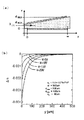
図15は本発明に係る電気光学素子の印加電圧とビーム偏向角およびビーム位置の変位量を表す図である。
同図において横軸は印加電圧を示し、縦軸は偏向角度及び変位量を示す。
25V程度の電圧印加により20°程度の大きなビーム偏向が可能となる。また広角にビーム光を走査した時であってもビーム変移量は電気光学結晶の幅より十分小さい。
Increasing the beam deflection angle due to the passage of the light beam through the electro-optic element increases the thickness difference of the wedge-shaped electro-optic crystal, that is, the difference between d max and d min, and further increases the width w of the electro-optic crystal. This is possible by making it smaller.
Accordingly, as another example of the dimensions of the electro-optical element, it is assumed that d max = 500 μm, d min = 40 μm, w = 500 μm, and L = 2.5 mm.
FIG. 15 is a diagram illustrating the applied voltage, the beam deflection angle, and the displacement amount of the beam position of the electro-optic element according to the present invention.
In the figure, the horizontal axis represents the applied voltage, and the vertical axis represents the deflection angle and the amount of displacement.
By applying a voltage of about 25V, a large beam deflection of about 20 ° is possible. Even when beam light is scanned at a wide angle, the beam displacement is sufficiently smaller than the width of the electro-optic crystal.
上記の例ではカー効果と空間電荷効果との組み合わせによるビーム偏向素子を示したが、ポッケルス効果と空間電荷効果とを組み合わせても同様に横方向(電気光学素子の両電極に平行な方向)に光ビームを走査する光偏向素子を実現することができる。
図16は本発明に係る電気光学素子の印加電圧とビーム偏向角およびビーム位置の変位量を表す図である。
ここで電気光学結晶基板の構造として、dmax=500μm、dmin=40μm、w=500μm、L=4.0mmを仮定した。また電気光学定数の値に関しては、図25における75℃での測定結果よりポッケルス係数rijは4000pm/V程度と見積もられるため、図16での計算でもrij=4000pm/Vを仮定した。図16より25V程度の電圧を印加することにより15°以上の広角のビーム走査が可能となることが分かる。またビーム位置の変移量も電気光学結晶の幅wより小さく出来ることも確認できる。
In the above example, a beam deflecting element based on a combination of the Kerr effect and space charge effect is shown. However, if the Pockels effect and space charge effect are combined, the beam deflection element is also in the horizontal direction (direction parallel to both electrodes of the electro-optic element). An optical deflection element that scans the light beam can be realized.
FIG. 16 is a diagram showing the applied voltage, the beam deflection angle, and the displacement amount of the beam position of the electro-optic element according to the present invention.
Here, as the structure of the electro-optic crystal substrate, d max = 500 μm, d min = 40 μm, w = 500 μm, and L = 4.0 mm were assumed. Regarding the value of the electro-optic constant, the Pockels coefficient r ij is estimated to be about 4000 pm / V from the measurement result at 75 ° C. in FIG. 25, and therefore, r ij = 4000 pm / V was assumed in the calculation in FIG. It can be seen from FIG. 16 that wide-angle beam scanning of 15 ° or more is possible by applying a voltage of about 25V. It can also be confirmed that the beam position shift amount can be made smaller than the width w of the electro-optic crystal.
〔第二の実施の形態(請求項1、3:楔形結晶の膜厚変化を曲線状にする)〕
図2を参照して本発明の第二の実施形態について述べる。
図2は本発明に係る電気光学素子の断面図を模式的に示した図であり、電気光学結晶0201の両面(図では上表面および下表面)にそれぞれ上部電極0202および下部電極0203を形成して成ることは図1に示した第一の実施形態と同様である。
ただし図1(b)においては電気光学結晶0101の厚さが直線状に変化しているのに対し、図2では電気光学結晶0201の厚さが曲線(例えば、指数関数曲線)状に変化させている点が異なる。言い換えると、本発明第一の実施形態では、電気光学結晶0101の厚さの変化率が一定であるのに対して、第二の実施形態では電気光学結晶0201の厚さの変化率が場所によって異なっていることに特徴がある。
[Second Embodiment (
A second embodiment of the present invention will be described with reference to FIG.
FIG. 2 is a diagram schematically showing a cross-sectional view of the electro-optic element according to the present invention, in which an
However, in FIG. 1B, the thickness of the electro-
本発明に係る第一の実施形態により、低電圧印加によって広角のビーム走査が可能であることを示したが、以下に示す課題も存在する。すなわち、光ビームの入射位置(y座標)が異なると、出射位置におけるビーム偏向角も異なるという問題点がある。
図17(a)は図2に示した電気光学素子の平面図をxy座標の第一象限に表示した図であり、図17(b)は光ビームの入射y座標を変化させたときの出射位置におけるビーム偏向角を比較した結果を示す図である。図17(b)において横軸は印加電圧を示し、縦軸は偏向角度を示す。
Although it has been shown that wide-angle beam scanning is possible by applying a low voltage according to the first embodiment of the present invention, the following problems also exist. That is, if the incident position (y coordinate) of the light beam is different, the beam deflection angle at the emission position is also different.
FIG. 17A is a diagram in which the plan view of the electro-optic element shown in FIG. 2 is displayed in the first quadrant of the xy coordinates, and FIG. 17B is the emission when the incident y coordinate of the light beam is changed. It is a figure which shows the result of having compared the beam deflection angle in a position. In FIG. 17B, the horizontal axis represents the applied voltage, and the vertical axis represents the deflection angle.
ここで光偏向素子の構造は図15の特性を得た際に用いた構造と同じであり、dmax=500μm、dmin=40μm、w=500μm、L=2.5mmである。ここで光ビームの入射y座標が0μm、10μm、20μmであるときの偏向角を比較すると入射y座標が大きいほど偏向角が小さい。すなわち素子の偏向性能が光ビームの入射位置に依存する。 Here, the structure of the optical deflection element is the same as that used when obtaining the characteristics shown in FIG. 15, and d max = 500 μm, d min = 40 μm, w = 500 μm, and L = 2.5 mm. Here, when the deflection angle when the incident y coordinate of the light beam is 0 μm, 10 μm, and 20 μm is compared, the larger the incident y coordinate, the smaller the deflection angle. That is, the deflection performance of the element depends on the incident position of the light beam.
この原因は以下の理由による。
ビームが出射する際の偏向角は、結晶内部に発生する屈折率変化量に依存する。より厳密には式(6)に示されるように、偏向角は屈折率変化量のy軸方向の微分の値に依存する。
The reason is as follows.
The deflection angle when the beam is emitted depends on the amount of change in the refractive index generated inside the crystal. More precisely, as shown in Expression (6), the deflection angle depends on the value of the derivative of the refractive index change amount in the y-axis direction.
ここで楔形光学結晶内部における屈折率変化を計算した結果である図13(b)を見ると、y座標が小さい領域での屈折率変化量が大きいことが分かる。したがって、ビーム偏向の多くはy座標の値が小さい領域を光が伝搬することによって発生する。すなわち、出来るだけy座標の小さい部分から光を入力することが、大きな偏向角を得るためには望ましい。
またy座標が小さい領域では屈折率変化量の微分量も座標に大きく依存するから、入射位置のずれに対して出射位置における偏向角の違いも大きくなる。
Here, looking at FIG. 13B, which is the result of calculating the refractive index change inside the wedge-shaped optical crystal, it can be seen that the amount of change in the refractive index in the region where the y coordinate is small is large. Therefore, most of the beam deflection is caused by light propagating through a region having a small y-coordinate value. That is, in order to obtain a large deflection angle, it is desirable to input light from a portion having as small a y coordinate as possible.
In the region where the y coordinate is small, the differential amount of the refractive index change greatly depends on the coordinate, so that the difference in the deflection angle at the exit position becomes large with respect to the deviation of the incident position.
y軸方向の入射位置のずれに対してビーム偏向角が変化しないようにするためには、y方向の変化に対して屈折率変化量Δnが線形に変化する必要がある。すなわち、dΔn/dyが一定の値になればよい。
図2に示すように、電気光学結晶の厚さを曲線状に変化させることで、上記のようなΔnの変化率の制御が可能になる。
図18(a)、(b)はその一例を示したものである。
図18(a)は図2に示した電気光学結晶の側面図をxy座標の第一象限に表示した図であり、図18(b)はy軸方向すなわち電気光学結晶の幅方向の変化に対する電気光学結晶内部での屈折率変化量を示した図であり、印加電圧をパラメータにしてある。また図18(b)にはy軸方向の変化に対する電気光学結晶の厚さも示してある。図18(b)において横軸はy座標における位置を示し、縦軸は屈折率変化及び厚さを示す。
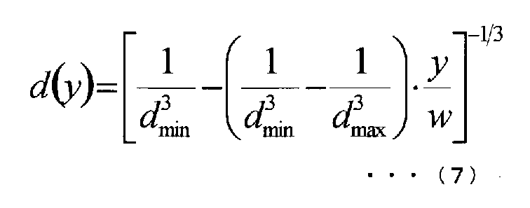
ここで電気光学結晶の厚さはy=0において最も薄い値(=dmin)をとり、y=wにおいて最も厚い値(=dmax)となるが、その間の厚さは式(7)の関係で変化させた。
In order to prevent the beam deflection angle from changing with respect to the deviation of the incident position in the y-axis direction, the refractive index change amount Δn needs to change linearly with respect to the change in the y-direction. That is, dΔn / dy may be a constant value.
As shown in FIG. 2, the rate of change of Δn as described above can be controlled by changing the thickness of the electro-optic crystal in a curved line.
FIGS. 18A and 18B show an example.
18A is a diagram in which the side view of the electro-optic crystal shown in FIG. 2 is displayed in the first quadrant of the xy coordinates, and FIG. 18B is a graph corresponding to a change in the y-axis direction, that is, the width direction of the electro-optic crystal. It is the figure which showed the refractive index variation | change_quantity inside an electro-optic crystal, and applied voltage is made into the parameter. FIG. 18B also shows the thickness of the electro-optic crystal with respect to the change in the y-axis direction. In FIG. 18B, the horizontal axis indicates the position in the y coordinate, and the vertical axis indicates the refractive index change and the thickness.
Here, the thickness of the electro-optic crystal takes the thinnest value (= d min ) at y = 0 and becomes the thickest value (= d max ) at y = w. Changed in relationship.
またここではカー効果と空間電荷効果とによって電気光学結晶内部に屈折変化が発した場合を考え、カー定数sij=1.0×10⁻¹⁴m2/V2を仮定した。その他の電気光学結晶の寸法はdmax=500μm、dmin=40μm、w=500μmを仮定した。また光ビームの入射x座標は20μmとした。
図18(b)より、印加電圧量の増加に対して屈折率変化量も増加し、またy軸方向の変化に対して電気光学結晶の屈折率も線形に変化していることがわかる。したがってこのときはy軸方向の入射位置のずれに対してビーム偏向角が変化せず、入射位置のトレランスが拡大することになる。
Here, a case where a refractive change occurs inside the electro-optic crystal due to the Kerr effect and the space charge effect, the Kerr constant s ij = 1.0 × 10 −14 m 2 / V 2 was assumed. The dimensions of other electro-optic crystals were assumed to be d max = 500 μm, d min = 40 μm, and w = 500 μm. The incident x coordinate of the light beam was 20 μm.
FIG. 18B shows that the amount of change in the refractive index increases as the amount of applied voltage increases, and the refractive index of the electro-optic crystal also changes linearly with respect to the change in the y-axis direction. Accordingly, at this time, the beam deflection angle does not change with respect to the deviation of the incident position in the y-axis direction, and the tolerance of the incident position is increased.
図19は本発明に係る電気光学素子の印加電圧とビーム偏向角およびビーム位置の変移量との関係を示す図であり、上記で仮定したパラメータの値に加えて相互作用長Lを6mmとした。図19において横軸は印加電圧を示し、縦軸は偏向角度を示す。
25V程度の電圧印加量で15°程度の広角なビーム走査が可能であり、そのときのビーム変移量Δyも結晶幅wと比べて小さくできる。この結果より本発明の第二の実施形態により、入射ビーム位置のずれに対してトレランスが広く、また低電圧駆動で広角にビーム走査が可能な光偏向素子が可能であることが示された。
また、図2では光学結晶の上面のみを曲線状にして結晶厚を変化させているが、結晶の下面のみや上下面両方に曲面を与えて結晶厚を変化させてもよい。
FIG. 19 is a diagram showing the relationship between the applied voltage of the electro-optic element according to the present invention, the deflection amount of the beam deflection, and the shift amount of the beam position. In addition to the parameter values assumed above, the interaction length L is set to 6 mm. . In FIG. 19, the horizontal axis indicates the applied voltage, and the vertical axis indicates the deflection angle.
Wide-angle beam scanning of about 15 ° is possible with a voltage application amount of about 25 V, and the beam shift amount Δy at that time can also be made smaller than the crystal width w. From this result, it was shown that the second embodiment of the present invention can provide an optical deflection element that has a wide tolerance with respect to the deviation of the incident beam position and can scan the beam at a wide angle with low voltage driving.
In FIG. 2, only the upper surface of the optical crystal is curved to change the crystal thickness. However, the crystal thickness may be changed by giving curved surfaces only to the lower surface or both the upper and lower surfaces of the crystal.
〔第三の実施の形態(請求項4:楔形結晶の膜厚変化を階段状にする)〕
図3に本発明の第三の実施形態を示す。
図3は本発明に係る電気光学素子を用いた光偏向器の断面図を模式的に示したものである。
同図に示す光偏向器は、電気光学結晶0301の両面(図では上表面および下表面)にそれぞれ上部電極0302および下部電極0303を形成して成る。さらに、光学結晶0301の厚さが電気光学結晶0301の幅方向に対して階段状に変化している。
[Third Embodiment (Claim 4: Wedge-shaped crystal thickness change is stepped)]
FIG. 3 shows a third embodiment of the present invention.
FIG. 3 schematically shows a cross-sectional view of an optical deflector using the electro-optic element according to the present invention.
The optical deflector shown in the figure is formed by forming an
図2に示した電気光学結晶0201の板厚を曲線状に変化させる構造を実現するためには高精度な加工技術が必要となる。そこでより加工を単純化するために、図3に示すような階段状に電気光学結晶0301の厚さを変化させることが有効である。
個々の段の幅を狭くすることで、局所的に見れば電気光学結晶0301は一定の厚さを持つものの、電気光学素子全体で見れば電気光学結晶0301の厚が曲線状に変化していることと等価になる。すなわち曲線状に電気光学結晶0301の厚さを変化させるのと同様の効果を得ることができる。
In order to realize a structure in which the thickness of the electro-
By narrowing the width of each step, the electro-
電気光学結晶0301の加工法の一例としては、基板厚が最も厚いところまでは、研磨等で一様に電気光学結晶を薄板化加工した後、ドライエッチング技術により所望の厚さまで電気光学結晶をエッチングする。エッチング時のマスクとして、フォトリソグラフィ等でパターニングを施したレジストを用いることができ、さらにレジストの厚さを段階的に変化させることでエッチング後の電気光学結晶0301の厚を変化させることができる。
As an example of a processing method of the electro-
〔第四の実施の形態(請求項5:光学結晶の密度を変える(微小パターンを施す))〕
図4(a)、(b)に本発明の第四の実施形態を示す。
図4(a)は本発明に係る電気光学素子の断面図を模式的に示したものであり、図4(b)は図4(a)に示した第四の実施形態の変形例を示す断面図である。
電気光学素子は、電気光学結晶0401の両面(図の上表面および下表面)にそれぞれ上部電極402および下部電極0403を形成して成る。また電気光学結晶0401の中に、電気光学結晶0401を厚さ方向に貫くように絶縁層0406を形成している。またここでは絶縁層0406の密度すなわち電気光学結晶0401の内部に含まれる絶縁層0406の割合は電気光学素子の断面の電圧源0404側(図の左側)ほど大きく、電圧源0404から離れるほど(図の右側に行くほど)小さくしている。
[Fourth Embodiment (Claim 5: Changing the density of an optical crystal (applying a minute pattern))]
4 (a) and 4 (b) show a fourth embodiment of the present invention.
FIG. 4A schematically shows a cross-sectional view of the electro-optical element according to the present invention, and FIG. 4B shows a modification of the fourth embodiment shown in FIG. 4A. It is sectional drawing.
The electro-optic element is formed by forming an upper electrode 402 and a
絶縁層0406は絶縁層0406の内部に電界を形成したときの屈折率変化量が電気光学結晶0401の屈折率変化量よりも小さい材料からなる。さらに絶縁層0406の屈折率は電気光学結晶0401と比較的近いことが好ましく、具体的には五酸化二タンタル(Ta2O5)を高濃度にドープした石英ガラスや、窒化シリコン(SiN)等の高屈折率ガラスや高屈折率ポリマー等が好適である。
The insulating
図4(a)に示した構造において、上部電極0402−下部電極0403間に電圧源0404から電圧を印加すると、電気光学結晶0401には電荷が注入され電界が形成されることにより、屈折率変化が生じる。これに対して、絶縁層0406には電圧が印加されても屈折率変化は生じない。
この原因として、一つには電気光学結晶0401と比べて絶縁層0406の材料内部に電荷が注入されにくくなることが考えられる。さらには仮に電荷が注入され、絶縁層0406内部に電界が形成されたとしても、そのことによる屈折率変化量は電気光学結晶0401の屈折率変化量と比べて極端に小さい。このため電気光学素子に電圧を印加した際、絶縁層0406の割合が大きい領域では、絶縁層0406の割合が小さい領域に比べて相対的に屈折率変化量が小さい。
In the structure shown in FIG. 4A, when a voltage is applied from the
One possible reason for this is that charges are less likely to be injected into the material of the insulating
図4(a)では電気光学素子の電圧源0404から離れるほど(図の右側の領域ほど)絶縁層0406が多く含まれるから、電気光学結晶0401に負の屈折率変化を与えるように正の電圧を印加したときには、相対的に右側の領域の方が等価的な屈折率変化量の絶対値が小さい。
したがって電気光学素子の等価的な屈折率は図の左側の領域ほど小さく、図の右側に行くほど大きくなる。
ここで光ビームを等価的な屈折率の低い電気光学素子の断面の左側から入力すると、等価的な屈折率の大きい右側の領域に向かって偏向しながら伝搬する。
In FIG. 4A, the farther away from the
Therefore, the equivalent refractive index of the electro-optic element is smaller in the region on the left side of the figure and larger as it goes to the right side of the figure.
When the light beam is input from the left side of the cross section of the electro-optic element having a low equivalent refractive index, the light beam propagates while being deflected toward the right region having a high equivalent refractive index.
電気光学素子内部に作り出される屈折率分布は絶縁層0406の密度を調整することで制御可能である。したがって、本発明の第二の実施の形態に示したような、電気光学結晶の曲面に電圧を印加したときと同様な屈折率の分布も作り出すことができる。
The refractive index distribution created inside the electro-optic element can be controlled by adjusting the density of the insulating
図4(a)に示した構成を実現する製作プロセスの一例を以下に述べる。
始めに電気光学結晶0401の材料を研磨技術等により所望の厚さに加工する。低電圧での駆動のためには、電気光学結晶0401の材料を薄くすることが好ましく、具体的には数十μm程度の結晶厚が好適である。その後RIE(Reactive Ion Etching)、ICP(Inductivity Coupled Plasma)エッチング、NLD(Neutral Loop Discharge)プラズマエッチング、集束イオン(FIB(Focused Ion Beam))エッチング等のドライエッチング技術により結晶材料の一部を掘り抜く。次に掘り抜いた箇所を埋めるように絶縁層を成膜する。絶縁膜の成膜には、高屈折率ガラス材料の場合にはスパッタやCVD(Chemical Vapor Deposition)等を用いることが好適であり、ポリマー材料の場合にディップコート等の成膜が簡便である。最後に光学結晶材料の表面に成膜された絶縁材料を取り除く。これば素子表面全体を研磨すればよい。以上のプロセスで製作した光学結晶と絶縁材料の混合基板の上下表面に電極を成膜する。
An example of a manufacturing process for realizing the configuration shown in FIG.
First, the material of the electro-
電気光学結晶0401の両面(図4(b)の上表面および下表面)にそれぞれ上部電極0402および下部電極0403を形成して成る。また、電気光学結晶0401の上表面から一定の厚さまで微細な孔を設けてあり、その孔を電極材料で埋め込む。ここで必ずしも孔の深さ全てを電極材料で埋め込む必要はなく、孔の表面を覆う程度の膜厚を成膜するのみでも十分である。電気光学結晶0401の材料に微細孔を施す方法は図4(a)の構造を製作する際と同様に、ドライエッチング技術により形成でき、電極材料の成膜には蒸着やスパッタ、電解めっき等の成膜技術を用いることができる。
An
図4(b)に示した電気光学素子に電圧を印加すると、微小孔を形成した部分においては、相対的に電気光学結晶0401の厚さが薄いため、形成される電界の強度が大きくなる。したがってその箇所の屈折率変化量は大きい。図4(b)では図の左側の領域ほど孔の密度を大きくしているため、電気光学結晶0401に負の屈折率変化を与えるように正の電圧を印加したときには、電気光学素子の等価的な屈折率は図の左側の領域ほど小さく、右側に行くほど大きくなる。
ここで光ビームを等価的な屈折率の低い電気光学素子断面の左側から入力すると、等価的な屈折率の大きい右側の領域に向かって偏向しながら伝搬する。
When a voltage is applied to the electro-optic element shown in FIG. 4B, the strength of the electric field formed is increased because the electro-
If the light beam is input from the left side of the cross section of the electro-optic element having a low equivalent refractive index, the light beam propagates while being deflected toward the right region having a high equivalent refractive index.
電気光学素子内部に作り出される屈折率分布は絶縁層0406の密度を調整することで制御可能である。したがって、本発明の第二の実施形態に示したような、電気光学結晶の曲面に電圧を印加したときと同様な屈折率の分布も作り出すことができる。
図4(b)では電気光学結晶0401の上面にのみパターンを施してあるが、電気光学結晶0401の下面のみや上下面両方にパターンを施してもよい。
The refractive index distribution created inside the electro-optic element can be controlled by adjusting the density of the insulating
In FIG. 4B, the pattern is applied only to the upper surface of the electro-
〔第五の実施の形態(請求項6:光学結晶に分極反転パターンを施す)〕
図5に本発明の第五の実施形態を示す。
図5は本発明に係る電気光学素子の断面図を模式的に示した図である。
電気光学素子は、電気光学結晶0501の両面(図5の上表面および下表面)にそれぞれ上部電極502および下部電極0503を形成して成る。また電気光学結晶0501の中に、電気光学結晶0501の分極の方向が他の領域の逆である分極反転領域0506が設けられている。また分極反転領域のデューティ比、すなわち電気光学結晶0501の内部に含まれる分極反転領域の割合は電気光学素子の断面の電圧源0504側(図の左側)ほど小さく、右側に行くほど大きい。
[Fifth Embodiment (Claim 6: A polarization inversion pattern is applied to an optical crystal)]
FIG. 5 shows a fifth embodiment of the present invention.
FIG. 5 is a diagram schematically showing a cross-sectional view of the electro-optic element according to the present invention.
The electro-optic element is formed by forming an upper electrode 502 and a
分極反転を施した領域では、電圧印加に対する屈折率変化の符号が逆転する。すなわち、正の電圧を印加したとき、通常は負の屈折率変化が生じるのに対して、分極反転領域においては正の屈折率変化が生じる。また印加電圧が等しい時、その屈折率変化量の絶対値は等しい。
したがって分極反転領域をデューティ比1:1で形成すると、正負の屈折率変化がキャンセルされるため等価的な屈折率変化量はゼロになる。図5に示した電気光学素子では、図の左側の領域では分極反転領域が少なく、したがって正の電圧印加に対して負の屈折率変化が生じる。これに対して図の右側の領域ほど、分極反転の領域が多いため、屈折率変化量は小さく、右端では等価的な屈折率変化量はゼロになる。
In the region where the polarization is reversed, the sign of the refractive index change with respect to the voltage application is reversed. That is, when a positive voltage is applied, a negative refractive index change usually occurs, whereas a positive refractive index change occurs in the domain-inverted region. When the applied voltages are equal, the absolute values of the refractive index change amounts are equal.
Therefore, when the domain-inverted region is formed with a duty ratio of 1: 1, the change in the positive and negative refractive indexes is canceled, and the equivalent amount of change in the refractive index becomes zero. In the electro-optic element shown in FIG. 5, there are few domain-inverted regions in the region on the left side of the diagram, and therefore a negative refractive index change occurs when a positive voltage is applied. On the other hand, since the region on the right side of the figure has more polarization inversion regions, the refractive index change amount is small, and the equivalent refractive index change amount is zero at the right end.
ここで光ビームを等価的な屈折率の低い電気光学素子断面の左側から入力すると、等価的な屈折率の大きい右側の領域に向かって偏向しながら伝搬する。電圧を印加したときの電気光学結晶0501の内部の等価的な屈折率は分極反転領域のデューティ比を調整することで制御でき、したがって複雑な電気光学結晶0501の曲面に電圧を印加したときと同様な屈折率の分布も作り出すことも可能である。
If the light beam is input from the left side of the cross section of the electro-optic element having a low equivalent refractive index, the light beam propagates while being deflected toward the right region having a high equivalent refractive index. The equivalent refractive index inside the electro-
具体的な分極反転領域の形成方法としては、LNやLTを用いた擬似位相整合デバイスにおいて広く適用されている電界印加法を応用し、電圧印加用の電極幅を微細化して電界を形成する方法の他、結晶表面に細く絞った電子ビームを直接照射することにより微細な電極を形成する必要なくマイクロドメイン反転が可能となる電子ビーム分極反転法や、フェムト秒レーザパルス照射によって局所的な分極反転領域を結晶に形成する方法等が考えられる。 As a specific method for forming a domain-inverted region, a method of applying an electric field application method widely applied in a quasi phase matching device using LN or LT, and forming an electric field by reducing the electrode width for voltage application In addition, the electron beam polarization reversal method that enables micro domain reversal without the need to form fine electrodes by directly irradiating a finely focused electron beam on the crystal surface, and local polarization reversal by femtosecond laser pulse irradiation A method of forming a region in a crystal can be considered.
〔変形例(請求項7:電極材料の抵抗率が変化する)〕
上述した本発明の第一の実施の形態から第五の実施の形態までの例では、いずれも電気光学結晶基板に何らかの加工を施して、電気光学結晶内部に発生する屈折率変化を制御し、電圧源に近い方の領域(各図の左側の領域)では相対的に屈折率が低く、電圧源から遠い領域(右側の領域)では相対的に屈折率が大きい状態を作り出した。言い換えると電気光学結晶の板厚や等価的な電気光学効果を制御することで屈折率分布を生じさせていた。
ここで、電気光学結晶内部の屈折率分布を制御する方法として、上述の方法とは異なり、印加電圧を電気光学結晶の場所に応じて変化させることが考えられる。例えば、屈折率変化量を大きくしたい領域においては印加電圧を大きくし、逆に屈折率変化量を小さくしたい領域においては印加電圧の印加量を小さくすればよい。
[Modification (Claim 7: Resistivity of electrode material changes)]
In the examples from the first embodiment to the fifth embodiment of the present invention described above, any processing is performed on the electro-optic crystal substrate to control the refractive index change generated inside the electro-optic crystal, In the region closer to the voltage source (the left region in each figure), the refractive index was relatively low, and in the region far from the voltage source (the right region), a relatively high refractive index was created. In other words, the refractive index distribution is generated by controlling the thickness of the electro-optic crystal and the equivalent electro-optic effect.
Here, as a method for controlling the refractive index distribution inside the electro-optic crystal, unlike the above-described method, it is conceivable to change the applied voltage in accordance with the location of the electro-optic crystal. For example, the applied voltage may be increased in a region where the refractive index change amount is desired to be increased, and conversely, the applied voltage may be reduced in a region where the refractive index change amount is desired to be reduced.
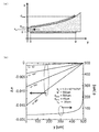
図19は電気光学結晶の幅方向に対して電気光学結晶内部の屈折率変化量を計算した一例である。
横軸に基板の幅方向の座標をy座標としてとり、縦軸として電気光学結晶内部に引き起こされる屈折率変化量を左軸にとっている。また、右軸にはあるy座標における電圧印加量を電気光学結晶に印加される最大の電圧Vmaxで規格化して取っている。ここでy座標に依存して変化する印加電圧V(y)は式(8)とした。
FIG. 19 shows an example in which the amount of change in the refractive index inside the electro-optic crystal is calculated with respect to the width direction of the electro-optic crystal.
The horizontal axis is the coordinate in the width direction of the substrate as the y coordinate, and the vertical axis is the amount of change in the refractive index caused inside the electro-optic crystal on the left axis. On the right axis, the voltage application amount at a certain y coordinate is standardized by the maximum voltage V max applied to the electro-optic crystal. Here, the applied voltage V (y) that changes depending on the y-coordinate is expressed by equation (8).
また、ここではカー効果と空間電荷効果とによって電気光学結晶内部に屈折変化が発した場合を考え、カー定数sij=1.0×10⁻¹⁴m2/V2を仮定した。その他の電気光学結晶の寸法は結晶厚をd=40μm、結晶幅w=500μmを仮定した。また光ビームの入射x座標は20μmとした。図19より、印加電圧量の増加に対して屈折率変化量も増加し、またy軸方向の変化に対して電気光学結晶の屈折率も線形に変化していることがわかる。したがってこのときはy軸方向の入射位置のずれに対してビーム偏向角が変化せず、入射位置のトレランスを拡大することができる。 Here, a case where a refractive change occurs inside the electro-optic crystal due to the Kerr effect and the space charge effect is assumed, and a Kerr constant s ij = 1.0 × 10 −14 m 2 / V 2 is assumed. As for the dimensions of the other electro-optic crystals, the crystal thickness was assumed to be d = 40 μm and the crystal width w = 500 μm. The incident x coordinate of the light beam was 20 μm. From FIG. 19, it can be seen that the amount of change in refractive index increases as the amount of applied voltage increases, and the refractive index of the electro-optic crystal also changes linearly with respect to the change in the y-axis direction. Therefore, at this time, the beam deflection angle does not change with respect to the deviation of the incident position in the y-axis direction, and the tolerance of the incident position can be increased.
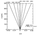
図20は図2に示した電気光学素子の電気光学結晶の幅方向の屈折率変化及び印加電圧との関係を示す図である。図20において横軸はy座標の位置を示し、縦軸は屈折率変化及び印加電圧を示す。
最大印加電圧を10V、20V、30Vと変化させることにより屈折率の変化率が急峻になることが分かる。
FIG. 20 is a diagram showing the relationship between the refractive index change in the width direction of the electro-optic crystal of the electro-optic element shown in FIG. 2 and the applied voltage. In FIG. 20, the horizontal axis indicates the y-coordinate position, and the vertical axis indicates the refractive index change and the applied voltage.
It can be seen that by changing the maximum applied voltage to 10V, 20V, and 30V, the refractive index change rate becomes steep.
図21は図2に示した電気光学素子の印加電圧とビーム偏向角およびビーム位置の変移量の関係を示す図であり、上記で仮定したパラメータの値に加えて相互作用長Lを8mmとした。20V程度の電圧印加量で15°程度の広角なビーム走査が可能であり、そのときのビーム変移量Δyも結晶幅wと比べて小さくできる。
以上のように、電圧印加量を電気光学結晶の幅方向で変化させることにより、入射ビーム位置のずれに対してトレランスが広く、また低電圧駆動で広角にビーム走査が可能な電気光学素子が可能であることが示された。
以下に、電気光学結晶内部に印加する電圧量を変化させる方法について述べる。
FIG. 21 is a diagram showing the relationship between the applied voltage of the electro-optic element shown in FIG. 2, the beam deflection angle, and the beam position shift amount. In addition to the parameter values assumed above, the interaction length L is 8 mm. . Wide-angle beam scanning of about 15 ° is possible with a voltage application amount of about 20 V, and the beam shift amount Δy at that time can also be made smaller than the crystal width w.
As described above, by changing the voltage application amount in the width direction of the electro-optic crystal, an electro-optic element that has a wide tolerance against the deviation of the incident beam position and can scan the beam at a wide angle by driving at a low voltage is possible. It was shown that.
A method for changing the amount of voltage applied to the inside of the electro-optic crystal will be described below.
〔第六の実施の形態〕
図6に本発明の第六の実施形態を示す。
図6は本発明に係る電気光学素子の断面図を模式的に示した図である。
電気光学素子は、電気光学結晶0601の両面(図の上表面および下表面)にそれぞれ上部電極0602および下部電極0603を形成して成る。
ここで、上部電極0602を形成する電極材料はある程度の電気抵抗値を有し、かつその抵抗値が電気光学結晶0601の幅方向に変化している。電気抵抗の大きな部分では電極内部を電流が通過する際に電圧が降下するため、例えば図6に示した電気光学素子において、電圧源0604から離れた領域(より右側の領域)ほど電気抵抗が大きくなるような電極材料を形成すれば、電気光学結晶0601に印加される電圧はより右側の領域ほど小さくなる。電気光学結晶0601に正の電圧を印加した場合、負の屈折率変化が発生するから、このときは右側の領域ほど相対的に屈折率が大きくなる。
ここで光ビームを等価的に屈折率の低い電気光学素子の断面の左側から入力すると、等価的に屈折率の大きい右側の領域に向かって偏向しながら伝搬する。
[Sixth embodiment]
FIG. 6 shows a sixth embodiment of the present invention.
FIG. 6 is a diagram schematically showing a cross-sectional view of the electro-optic element according to the present invention.
The electro-optic element is formed by forming an
Here, the electrode material forming the
Here, when the light beam is input from the left side of the cross section of the electro-optic element having an equivalent low refractive index, the light beam propagates while being deflected toward the right region having an equivalent high refractive index.
電気抵抗の大小を制御する一例として、電極材料中に異種の材料をドープする方法がある。例えば、電気抵抗の小さい材料(抵抗率1Ωcm以下、例えば、銅)で電極を形成した後、高い電気抵抗値を有する材料(抵抗率1GΩcm以上、例えば、Si)を右側の領域ほど高濃度になるようにドープすることで、電極全体では右側の領域ほど電気抵抗が大きくなる。または電気抵抗値の大きさは同程度であっても、その温度依存性が異なる2種類の電極材料を組み合わせてもよい。例えば温度依存性の小さな材料で電極を形成した後、温度依存性の大きな材料を右側の領域ほど高濃度になるようにドープする。電気光学素子の動作時には電極を一定の温度に加熱あるいは冷却することにより、電極の電気抵抗に分布を持たせることが可能となる。
As an example of controlling the magnitude of electric resistance, there is a method of doping a different material into an electrode material. For example, after an electrode is formed of a material having a low electrical resistance (
〔第七の実施の形態(請求項8:電極に微細パターンを施して等価的な電界形成量を制御する)〕
電気抵抗が場所によって異なることと同様の状態は一種類の電極材料によっても作り出すことが可能である。
図7(a)〜(c)は本発明に係る電気光学素子の第七の実施形態を示したものである。図7(a)および図7(b)は電気光学素子を上面からみたときの様子を示し、図7(c)は図7(a)および図7(b)におけるVIIc−VIIc線での電気光学素子断面の様子を模式的に表した図である。
電気光学素子は電気光学結晶0701の両面(図7(c)の上表面および下表面)にそれぞれ上部電極0702および下部電極0703を形成して成る。
ここで上部電極0702には微細なパターンが形成され、そのパターンにおいては電気光学結晶0701の表面に電極材料が存在しない。また微細パターンにおいて電気光学結晶0701の表面に電極材料が存在しない領域の密度は電圧源0704から離れるほど(図の右側の領域になるほど)大きい。この密度を変化させる例として、図7(a)では微細な円孔パターンの配置密度を変化させ、図7(b)ではパターンを形成する孔の径を変化させている。図7(a)および図7(b)では円孔パターンの例を示したが、電気光学素子の領域に応じて電極材料が存在する領域の面密度が変化する限りにおいてパターンの形状は任意である。
[Seventh Embodiment (Claim 8: An equivalent electric field formation amount is controlled by applying a fine pattern to an electrode)]
A state similar to the fact that the electrical resistance varies from place to place can also be created with one kind of electrode material.
7A to 7C show a seventh embodiment of the electro-optic element according to the present invention. FIGS. 7A and 7B show the state of the electro-optic element when viewed from the top, and FIG. 7C shows the electricity at the line VIIc-VIIc in FIGS. 7A and 7B. It is the figure which represented the mode of the optical element cross section typically.
The electro-optic element is formed by forming an
Here, a fine pattern is formed on the
ビーム偏向が発生する原因は、電極から電気光学結晶0701の内部に電荷が注入されることである。したがって、電気光学結晶0701の表面に電極が存在しない微細パターンにおいては電荷が注入されず、そのような領域では同じ電圧を印加した場合であっても電気光学結晶0701の内部に形成される電界強度は小さくなる。
したがって図7に示した電気光学素子においてはより右側の領域になるほど電荷の注入量が減少し、電圧印加によって引き起こされる屈折率変化量は小さくなる。正の電圧を印加した場合、負の屈折率変化が発生するから、右側の領域ほど相対的に屈折率が大きくなり、ここで光ビームを等価的に屈折率の低い電気光学素子の断面の左側から入力すると、等価的に屈折率の大きい右側の領域に向かって偏向しながら伝搬する。
The cause of the beam deflection is that electric charges are injected from the electrodes into the electro-
Therefore, in the electro-optical element shown in FIG. 7, the amount of charge injection decreases as the region is on the right side, and the amount of change in refractive index caused by voltage application decreases. When a positive voltage is applied, a negative refractive index change occurs. Therefore, the refractive index increases relatively in the right region, and the light beam is equivalent to the left side of the cross section of the electro-optic element whose refractive index is low. Is input while being deflected toward the right region having a large refractive index equivalently.
〔第八の実施の形態(請求項9:電極にストライプパターンを施して等価的な電界形成量を制御する)〕
図8は本発明に係る電気光学素子の第八の実施形態を示したものである。
図8は電気光学素子を上面からみた様子を模式的に表した図である。また、ここでは図示しないが、電気光学素子の断面構造は図7(c)に等しい。図7(a)〜(c)に示した第七の実施形態では電極に微細なパターンを付与したが、電極のパターンとして図8に示すようなストライプ形状のものも有効である。このとき電極の幅が広いほど電荷の注入量が多くなり、結果として電圧印加によって生じる屈折率変化量が大きくなる。
したがって図8に示すように、ストライプ線幅の狭い右側の領域ほど屈折率変化量が小さくなるため、正の電圧を印加したとき、右側の領域ほど屈折率が大きくなる。
ここで光ビームを等価的に屈折率の低い電気光学素子の断面のストライプ間隔の短い側(図の左側)から入力すると、等価的に屈折率の大きい右側の領域に向かって偏向しながら伝搬する。
[Eighth Embodiment (Claim 9: An equivalent electric field formation amount is controlled by applying a stripe pattern to an electrode)]
FIG. 8 shows an eighth embodiment of an electro-optic element according to the present invention.
FIG. 8 is a diagram schematically showing a state in which the electro-optic element is viewed from above. Although not shown here, the cross-sectional structure of the electro-optic element is equal to that shown in FIG. In the seventh embodiment shown in FIGS. 7A to 7C, a fine pattern is given to the electrode. However, a stripe shape as shown in FIG. 8 is also effective as the electrode pattern. At this time, the wider the width of the electrode, the larger the amount of injected charge, resulting in a larger amount of refractive index change caused by voltage application.
Therefore, as shown in FIG. 8, since the amount of change in the refractive index is smaller in the right region having a narrower stripe line width, the refractive index is larger in the right region when a positive voltage is applied.
Here, if the light beam is input from the side of the cross section of the electro-optic element having an equivalently low refractive index with a short stripe interval (the left side in the figure), it propagates while being deflected toward the right region having an equivalently large refractive index. .
〔第九の実施の形態(請求項10:電極材料が2種類以上の材料から成る)〕
図9(a)、(b)は本発明の第九の実施形態を示す。
本発明に係る電気光学素子を上面からみた様子を図9(a)に表し、またIXb−Ixb線における断面構造を図9(b)に模式的に表す。
電気光学素子は電気光学結晶0901の一方の面(図9(a)の上表面)に第1の上部電極0902および第2の上部電極0904が形成され、また電気光学結晶0901の他方の面(図9(a)の下表面)に下部電極0905が形成されて成る。
ここで第1の上部電極0902には微細なパターンが施され、さらに電気光学結晶0901と第1の上部電極0902とを同時に覆うように第2の上部電極層0903が形成される。
[Ninth Embodiment (Claim 10: Electrode material comprises two or more kinds of materials)]
9 (a) and 9 (b) show a ninth embodiment of the present invention.
FIG. 9A shows a state of the electro-optic element according to the present invention as viewed from above, and FIG. 9B schematically shows a cross-sectional structure taken along line IXb-Ixb.
In the electro-optic element, the first
Here, a fine pattern is applied to the first
第七の実施形態で示したように、電極に微細なパターンを形成することにより、電気光学結晶0901の内部に形成される電界の制御が可能となるが、微細パターンの形状によっては電極パターン同士が分断されてしまい、互いに等しい電圧を印加することが困難となる場合がある。例えば、微細パターンが円孔ではなく、円ドットとなる場合などが考えられる。この場合、微細パターンを第2の上部電極0903で埋め込むことで、第2の上部電極0903に電圧を印加すれば第1の上部電極0902を形成する微細パターン全体に等しい電圧を印加させることができる。
As shown in the seventh embodiment, it is possible to control the electric field formed in the electro-
空間電荷効果を発生させるためには、電気光学結晶0901と電極材料とがオーミック接触により接触していることが必要である。そのため、第1の上部電極0902と第2の上部電極0903とで互いの仕事関数が異なるような電極材料を選択すれば、オーミック接触となる領域がより多くの電荷が注入され、結果的にその領域の屈折率変化量が大きくなる。例えば、図9(a)、(b)において、第1の上部電極0902の材料として、電気光学結晶0901とのオーミック接触を実現するようにTiやCrなどの仕事関数の大きな電極材料を用い、かつ第2の上部電極0903の材料としてAuやPt等の仕事関数の小さな電極材料を用いる。このとき第2の上部電極0902の材料と電気光学結晶0901とが接触する部分の大きな領域(図9(b)の右側の領域)は、相対的に電荷の注入量が小さいため屈折率変化量が小さくなる。
したがって正の電圧を印加したとき、右側の領域ほど屈折率が大きくなる。
ここで光ビームを等価的に屈折率の低い電気光学素子の断面の左側から入力すると、等価的に屈折率の大きい右側の領域に向かって偏向しながら伝搬する。
In order to generate the space charge effect, it is necessary that the electro-
Therefore, when a positive voltage is applied, the refractive index increases in the right region.
Here, when the light beam is input from the left side of the cross section of the electro-optic element having an equivalent low refractive index, the light beam propagates while being deflected toward the right region having an equivalent high refractive index.
以上に示した図6から図9(a)、(b)では全て上部電極にのみパターンを施してあるが、下部電極のみや上部電極及び下部電極の両電極にパターンを施してもよい。 In FIGS. 6 to 9A and 9B described above, the pattern is applied only to the upper electrode, but the pattern may be applied only to the lower electrode or both the upper electrode and the lower electrode.
〔第十の実施の形態(請求項11:電極と光学結晶の間に抵抗体を挿入する)〕
電気光学結晶の幅方向に異なる電圧量を印加する方法として、上部電極及び下部電極の材料と電気光学結晶との間に電気抵抗体層を挿入することも有効である。
図10は本発明の第十の実施形態を示したものである。
図10は本発明に係る電気光学素子の断面構造を模式的に表した図である。
電気光学素子は電気光学結晶1001の一方の面(図の下表面)に下部電極1003が形成され、電気光学素子1001の他方の面(図の上表面)には電気抵抗体1006および上部電極1002が順次積層されて成る。
ここで電気抵抗体1006は電気光学結晶1001の幅方向(図の横方向)にその電気抵抗値が変化するものである。
[Tenth embodiment (Claim 11: Inserting a resistor between an electrode and an optical crystal)]
As a method of applying different voltage amounts in the width direction of the electro-optic crystal, it is also effective to insert an electric resistor layer between the material of the upper electrode and the lower electrode and the electro-optic crystal.
FIG. 10 shows a tenth embodiment of the present invention.
FIG. 10 is a diagram schematically showing a cross-sectional structure of the electro-optic element according to the present invention.
In the electro-optic element, a
Here, the electric resistance value of the
上部電極1002−下部電極1003間に電圧を印加したとき、電気光学結晶1001には電気抵抗体1006を介して電圧が印加されるが、電気抵抗体1006を電流が流れる際にその抵抗値に応じた電圧低下が生じる。
例えば図10において、電圧源1004から離れるほど(図の右側の領域ほど)電気抵抗が大きいとすると、右側の領域ほど電気光学結晶1001に印加される電圧は低くなる。すなわち電気光学結晶1001の内部に形成される電界は小さくなる。したがって電気光学素子の右側の領域ほど相対的に電荷の注入量が小さいため屈折率変化量が小さくなる。したがって電気光学素子に正の電圧を印加したとき、右側の領域ほど屈折率が大きくなる。
ここで光ビームを等価的に屈折率の低い電気光学素子の断面の左側から入力すると、等価的に屈折率の大きい右側の領域に向かって偏向しながら伝搬する。
When a voltage is applied between the
For example, in FIG. 10, assuming that the electric resistance increases as the distance from the
Here, when the light beam is input from the left side of the cross section of the electro-optic element having an equivalent low refractive index, the light beam propagates while being deflected toward the right region having an equivalent high refractive index.
〔第十一の実施の形態(請求項12:電極と光学結晶の間に挿入した抵抗体の厚さを変化させる。)〕
電気抵抗体を構成する材料が全ての領域で同一の抵抗率を有している場合でも上記と同様の効果を得ることは可能である。
図11は本発明の第十一の実施形態を示す。
図11は本発明に係る電気光学素子の断面構造を模式的に表した図である。
電気光学素子は電気光学結晶1101の一方の面(図の下表面)に下部電極1103が形成され、電気光学結晶1101の他方の面(図の上表面)には電気抵抗体1106および上部電極1102が順次積層されて成る。
ここで電気抵抗体1106は電気光学結晶1101の幅方向(図の横方向)にその膜厚が変化する。
[Eleventh embodiment (Claim 12: The thickness of the resistor inserted between the electrode and the optical crystal is changed)]
Even when the material constituting the electric resistor has the same resistivity in all regions, the same effect as described above can be obtained.
FIG. 11 shows an eleventh embodiment of the present invention.
FIG. 11 is a diagram schematically showing a cross-sectional structure of the electro-optic element according to the present invention.
In the electro-optic element, a
Here, the thickness of the
電気抵抗体1106の材料の電気抵抗率が一定であれば、その厚さが厚い部分ほど電気抵抗が大きくなり、したがって電気光学結晶1101に印加される電圧は低くなり、電気光学結晶1101内部に形成される電界は小さくなる。図11では電圧源1104から離れるほど(右側の領域ほど)電気抵抗体1106の層の厚さが厚くなっているため、右側の領域ほど相対的に電荷の注入量が小さいため屈折率変化量が小さくなる。したがって、電気光学素子に正の電圧を印加したとき、右側の領域ほど屈折率が大きくなる。ここで光ビームを等価的に屈折率の低い電気光学素子の断面の左側から入力すると、等価的に屈折率の大きい右側の領域に向かって偏向しながら伝搬する。
If the electrical resistivity of the material of the
〔第十二の実施の形態(請求項13:電極と光学結晶の間に挿入した抵抗体の厚さを階段状に変化させる。)〕
図12は本発明の第十二の実施形態を示したものである。
図12は本発明に係る電気光学素子の断面構造を模式的に表した図である。
電気光学素子は電気光学結晶1201の一方の面(図の下表面)に下部電極1203が形成され、電気光学結晶1201の他方の面(図の上表面)には電気抵抗体1206および上部電極1202が順次積層されて成る。
ここで電気抵抗体1206は電気光学結晶1201の幅方向(図の横方向)にその膜厚が階段状に変化する。
[Twelfth embodiment (Claim 13: The thickness of the resistor inserted between the electrode and the optical crystal is changed stepwise)]
FIG. 12 shows a twelfth embodiment of the present invention.
FIG. 12 is a diagram schematically showing a cross-sectional structure of the electro-optic element according to the present invention.
In the electro-optic element, a
Here, the thickness of the
第十一の実施形態において、電気光学結晶内部に形成される電界分布を高精度に制御するためには、電気抵抗体1206の膜厚を、図11に示すような線形にではなく、より複雑な曲線状に変化させることが必要になる。図12に示すように電気抵抗体1206の層の膜厚を細かく段階的に変化させることにより、等価的に曲線状に膜厚が変化する電気抵抗体1106と同様の効果が期待できる。
In the eleventh embodiment, in order to control the electric field distribution formed in the electro-optic crystal with high accuracy, the film thickness of the
なお、上述した実施の形態は、本発明の好適な実施の形態の一例を示すものであり、本発明はそれに限定されることなく、その要旨を逸脱しない範囲内において、種々変形実施が可能である。
例えば、上述した実施の形態では電気光学素子の場合について説明したが、電気光学素子に光ビームを出射する光源(例えば、レーザ)を設けた光ビーム偏向器に適用してもよい。
The above-described embodiment shows an example of a preferred embodiment of the present invention, and the present invention is not limited thereto, and various modifications can be made without departing from the scope of the invention. is there.
For example, although the case of the electro-optic element has been described in the above-described embodiment, the present invention may be applied to a light beam deflector provided with a light source (for example, a laser) that emits a light beam to the electro-optic element.
0101 電気光学結晶
0102 上部電極
0103 下部電極
0104 電圧源
0105 光ビーム
0101 Electro-
Claims (14)
前記光伝搬領域の屈折率が可変であることを特徴とする電気光学素子。 In an electro-optic element in which an electrode region is formed on both surfaces of the substrate made of an electro-optic material, and light propagates in the electro-optic material between the electrode regions,
An electro-optical element, wherein a refractive index of the light propagation region is variable.
Priority Applications (1)
| Application Number | Priority Date | Filing Date | Title |
|---|---|---|---|
| JP2007264426A JP5006748B2 (en) | 2007-10-10 | 2007-10-10 | Electro-optic element and light beam deflector |
Applications Claiming Priority (1)
| Application Number | Priority Date | Filing Date | Title |
|---|---|---|---|
| JP2007264426A JP5006748B2 (en) | 2007-10-10 | 2007-10-10 | Electro-optic element and light beam deflector |
Publications (2)
| Publication Number | Publication Date |
|---|---|
| JP2009092995A true JP2009092995A (en) | 2009-04-30 |
| JP5006748B2 JP5006748B2 (en) | 2012-08-22 |
Family
ID=40665028
Family Applications (1)
| Application Number | Title | Priority Date | Filing Date |
|---|---|---|---|
| JP2007264426A Expired - Fee Related JP5006748B2 (en) | 2007-10-10 | 2007-10-10 | Electro-optic element and light beam deflector |
Country Status (1)
| Country | Link |
|---|---|
| JP (1) | JP5006748B2 (en) |
Cited By (4)
| Publication number | Priority date | Publication date | Assignee | Title |
|---|---|---|---|---|
| JP2010222240A (en) * | 2009-02-27 | 2010-10-07 | Nagaoka Univ Of Technology | Light modulation material and method for producing the same |
| JP2013104419A (en) * | 2011-11-17 | 2013-05-30 | Mitsubishi Electric Corp | Screw compressor |
| CN119828392A (en) * | 2025-02-18 | 2025-04-15 | 杭州芯河光电科技有限公司 | Scanning device and imaging system |
| CN119902401A (en) * | 2025-01-21 | 2025-04-29 | 山东省科学院新材料研究所 | A light deflection method and device based on barium strontium niobate crystal with gradient composition |
Citations (9)
| Publication number | Priority date | Publication date | Assignee | Title |
|---|---|---|---|---|
| JPS626230A (en) * | 1985-07-02 | 1987-01-13 | Brother Ind Ltd | Optical deflecting device |
| JPH01293324A (en) * | 1988-05-20 | 1989-11-27 | Minolta Camera Co Ltd | Optical modulator |
| JPH10282531A (en) * | 1997-04-08 | 1998-10-23 | Tdk Corp | Optical deflector |
| JP2002365676A (en) * | 2001-06-11 | 2002-12-18 | Mitsui Chemicals Inc | Optical deflecting element |
| JP2004118049A (en) * | 2002-09-27 | 2004-04-15 | Sharp Corp | Optical path conversion device |
| JP2004258169A (en) * | 2003-02-25 | 2004-09-16 | Alps Electric Co Ltd | Optical deflection element and optical switch using the same |
| JP2005024679A (en) * | 2003-06-30 | 2005-01-27 | Asahi Glass Co Ltd | Optical deflector and optical scanning device |
| JP2006267906A (en) * | 2005-03-25 | 2006-10-05 | Ricoh Co Ltd | Optical deflection element / image display device |
| WO2006137408A1 (en) * | 2005-06-20 | 2006-12-28 | Nippon Telegraph And Telephone Corporation | Electro-optical element |
-
2007
- 2007-10-10 JP JP2007264426A patent/JP5006748B2/en not_active Expired - Fee Related
Patent Citations (9)
| Publication number | Priority date | Publication date | Assignee | Title |
|---|---|---|---|---|
| JPS626230A (en) * | 1985-07-02 | 1987-01-13 | Brother Ind Ltd | Optical deflecting device |
| JPH01293324A (en) * | 1988-05-20 | 1989-11-27 | Minolta Camera Co Ltd | Optical modulator |
| JPH10282531A (en) * | 1997-04-08 | 1998-10-23 | Tdk Corp | Optical deflector |
| JP2002365676A (en) * | 2001-06-11 | 2002-12-18 | Mitsui Chemicals Inc | Optical deflecting element |
| JP2004118049A (en) * | 2002-09-27 | 2004-04-15 | Sharp Corp | Optical path conversion device |
| JP2004258169A (en) * | 2003-02-25 | 2004-09-16 | Alps Electric Co Ltd | Optical deflection element and optical switch using the same |
| JP2005024679A (en) * | 2003-06-30 | 2005-01-27 | Asahi Glass Co Ltd | Optical deflector and optical scanning device |
| JP2006267906A (en) * | 2005-03-25 | 2006-10-05 | Ricoh Co Ltd | Optical deflection element / image display device |
| WO2006137408A1 (en) * | 2005-06-20 | 2006-12-28 | Nippon Telegraph And Telephone Corporation | Electro-optical element |
Cited By (4)
| Publication number | Priority date | Publication date | Assignee | Title |
|---|---|---|---|---|
| JP2010222240A (en) * | 2009-02-27 | 2010-10-07 | Nagaoka Univ Of Technology | Light modulation material and method for producing the same |
| JP2013104419A (en) * | 2011-11-17 | 2013-05-30 | Mitsubishi Electric Corp | Screw compressor |
| CN119902401A (en) * | 2025-01-21 | 2025-04-29 | 山东省科学院新材料研究所 | A light deflection method and device based on barium strontium niobate crystal with gradient composition |
| CN119828392A (en) * | 2025-02-18 | 2025-04-15 | 杭州芯河光电科技有限公司 | Scanning device and imaging system |
Also Published As
| Publication number | Publication date |
|---|---|
| JP5006748B2 (en) | 2012-08-22 |
Similar Documents
| Publication | Publication Date | Title |
|---|---|---|
| KR101363125B1 (en) | Electro-optical element | |
| JP4751389B2 (en) | Beam deflector | |
| JP5130810B2 (en) | Optical deflector | |
| US8483523B2 (en) | Optical waveguide electro-optic device and process of manufacturing optical waveguide electro-optic device | |
| JP5006748B2 (en) | Electro-optic element and light beam deflector | |
| JP2013140328A (en) | Optical device, optical deflector, and optical modulator | |
| US9291874B2 (en) | Optical deflection element and optical deflection device | |
| JP2010026079A (en) | Optical device | |
| US7580594B2 (en) | Optical modulation element and optical modulation device having the same | |
| JP4672331B2 (en) | Optical deflection element and optical switch | |
| US8400703B2 (en) | Optical switch | |
| US7976717B2 (en) | Method of forming polarization reversal area, apparatus thereof and device using it | |
| JP2012159584A (en) | Electro-optical element | |
| JP2013044762A (en) | Electro-optical element and manufacturing method thereof, and optical deflection device using electro-optical element | |
| KR20240032837A (en) | High-speed active beam-steering devices and devices operating in transmission mode | |
| JP5416022B2 (en) | Frequency independent optical deflector | |
| US12265311B2 (en) | Electro-optical device | |
| JP2012155045A (en) | Electro-optic element and production method of the same | |
| US20260126700A1 (en) | Waveguide arrangement and method for deflecting at least one light beam or light beam pair | |
| JP7514131B2 (en) | Optical control device and driving method thereof | |
| JP2006154145A (en) | Optical element and optical switch | |
| Kutteeri et al. | Two-dimensional beam steering by cascaded domain engineering in lithium niobate | |
| JP6322883B2 (en) | Optical deflection element | |
| JP4663604B2 (en) | Electro-optic element | |
| JP2012108377A (en) | Light deflector |
Legal Events
| Date | Code | Title | Description |
|---|---|---|---|
| A621 | Written request for application examination |
Free format text: JAPANESE INTERMEDIATE CODE: A621 Effective date: 20100803 |
|
| A131 | Notification of reasons for refusal |
Free format text: JAPANESE INTERMEDIATE CODE: A131 Effective date: 20111004 |
|
| A521 | Written amendment |
Free format text: JAPANESE INTERMEDIATE CODE: A523 Effective date: 20111201 |
|
| TRDD | Decision of grant or rejection written | ||
| A01 | Written decision to grant a patent or to grant a registration (utility model) |
Free format text: JAPANESE INTERMEDIATE CODE: A01 Effective date: 20120522 |
|
| A01 | Written decision to grant a patent or to grant a registration (utility model) |
Free format text: JAPANESE INTERMEDIATE CODE: A01 |
|
| A61 | First payment of annual fees (during grant procedure) |
Free format text: JAPANESE INTERMEDIATE CODE: A61 Effective date: 20120525 |
|
| FPAY | Renewal fee payment (event date is renewal date of database) |
Free format text: PAYMENT UNTIL: 20150601 Year of fee payment: 3 |
|
| R150 | Certificate of patent or registration of utility model |
Ref document number: 5006748 Country of ref document: JP Free format text: JAPANESE INTERMEDIATE CODE: R150 Free format text: JAPANESE INTERMEDIATE CODE: R150 |
|
| LAPS | Cancellation because of no payment of annual fees |