JP2009093105A - マイクロミラー装置、およびミラー部形成方法 - Google Patents
マイクロミラー装置、およびミラー部形成方法 Download PDFInfo
- Publication number
- JP2009093105A JP2009093105A JP2007266190A JP2007266190A JP2009093105A JP 2009093105 A JP2009093105 A JP 2009093105A JP 2007266190 A JP2007266190 A JP 2007266190A JP 2007266190 A JP2007266190 A JP 2007266190A JP 2009093105 A JP2009093105 A JP 2009093105A
- Authority
- JP
- Japan
- Prior art keywords
- mirror
- micromirror device
- film thickness
- forming
- mask pattern
- Prior art date
- Legal status (The legal status is an assumption and is not a legal conclusion. Google has not performed a legal analysis and makes no representation as to the accuracy of the status listed.)
- Withdrawn
Links
- 238000000034 method Methods 0.000 title claims description 22
- 230000002093 peripheral effect Effects 0.000 claims abstract description 13
- 239000010408 film Substances 0.000 description 25
- 229910021421 monocrystalline silicon Inorganic materials 0.000 description 18
- VYPSYNLAJGMNEJ-UHFFFAOYSA-N Silicium dioxide Chemical compound O=[Si]=O VYPSYNLAJGMNEJ-UHFFFAOYSA-N 0.000 description 14
- 239000000758 substrate Substances 0.000 description 13
- KWYUFKZDYYNOTN-UHFFFAOYSA-M Potassium hydroxide Chemical compound [OH-].[K+] KWYUFKZDYYNOTN-UHFFFAOYSA-M 0.000 description 12
- 238000005530 etching Methods 0.000 description 11
- 229910004298 SiO 2 Inorganic materials 0.000 description 10
- 230000008569 process Effects 0.000 description 10
- 238000004519 manufacturing process Methods 0.000 description 9
- 229910052681 coesite Inorganic materials 0.000 description 7
- 229910052906 cristobalite Inorganic materials 0.000 description 7
- 239000000377 silicon dioxide Substances 0.000 description 7
- 235000012239 silicon dioxide Nutrition 0.000 description 7
- 229910052682 stishovite Inorganic materials 0.000 description 7
- 229910052905 tridymite Inorganic materials 0.000 description 7
- 230000015572 biosynthetic process Effects 0.000 description 4
- 229910052751 metal Inorganic materials 0.000 description 4
- 239000002184 metal Substances 0.000 description 4
- 230000004044 response Effects 0.000 description 4
- 238000001020 plasma etching Methods 0.000 description 3
- 230000000694 effects Effects 0.000 description 2
- 230000003287 optical effect Effects 0.000 description 2
- 238000000059 patterning Methods 0.000 description 2
- 125000006850 spacer group Chemical group 0.000 description 2
- XUIMIQQOPSSXEZ-UHFFFAOYSA-N Silicon Chemical compound [Si] XUIMIQQOPSSXEZ-UHFFFAOYSA-N 0.000 description 1
- 238000005452 bending Methods 0.000 description 1
- 230000008901 benefit Effects 0.000 description 1
- 238000005516 engineering process Methods 0.000 description 1
- 238000005755 formation reaction Methods 0.000 description 1
- 239000011521 glass Substances 0.000 description 1
- 238000001465 metallisation Methods 0.000 description 1
- 239000000203 mixture Substances 0.000 description 1
- 230000003647 oxidation Effects 0.000 description 1
- 238000007254 oxidation reaction Methods 0.000 description 1
- 230000009467 reduction Effects 0.000 description 1
- 239000004065 semiconductor Substances 0.000 description 1
- 229910052710 silicon Inorganic materials 0.000 description 1
- 239000010703 silicon Substances 0.000 description 1
- 239000010409 thin film Substances 0.000 description 1
- 239000013585 weight reducing agent Substances 0.000 description 1
Images

Landscapes
- Facsimile Heads (AREA)
- Mechanical Optical Scanning Systems (AREA)
Abstract
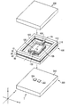
【解決手段】光源からの光を走査光として反射するミラー部を備え、当該ミラー部の中央部の膜厚が当該ミラー部の周辺部の膜厚よりも薄くなるよう形成されたマイクロミラー装置を提供する。
【選択図】図1
Description
100 マイクロミラーデバイス部
110 枠部
120 ミラー部
122 ミラー面
124 ミラー裏面
126 リブ
130 トーションバー
200 蓋部
300 下部基板
Claims (5)
- 光を走査するマイクロミラー装置において、
光源からの光を走査光として反射するミラー部を備え、
前記ミラー部の中央部の膜厚が当該ミラー部の周辺部の膜厚よりも薄くなるよう形成されたこと、を特徴とするマイクロミラー装置。 - 前記ミラー部において、該光源からの光を反射するミラー面と、前記ミラー面の裏面の少なくとも一方の面上で、該周辺部の少なくとも一部分が前記ミラー部の中央部よりも突出して形成されたこと、を特徴とする請求項1に記載のマイクロミラー装置。
- 前記ミラー部の中央部は、前記ミラー面上の光学的な有効領域を含むこと、を特徴とする請求項1又は請求項2の何れかに記載のマイクロミラー装置。
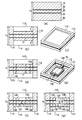
- 基台に対して揺動可能に支持されるミラー部を形成するミラー部形成方法において、
該基台表面の所定領域に第1のマスクパターンを形成する第1のマスクパターン形成ステップと、
前記第1のマスクパターンから露出した領域を除去して前記ミラー部に対応したミラー形状を形成するミラー形状形成ステップと、
前記ミラー形状に対応する領域のうち当該ミラー形状の周辺領域のみに第2のマスクパターンを形成する第2のマスクパターン形成ステップと、
前記第2のマスクパターンから露出した前記ミラー形状の中央領域を所定の深さだけ除去して、当該中央領域の膜厚を該ミラー形状の周辺領域の膜厚よりも薄肉に形成する薄肉形成ステップと、を含むミラー部形成方法。 - 該基台はエッチストップ層を含み、
前記薄肉形成ステップにおいて、該中央領域の膜厚がエッチストップ層で規定される、ミラー部形成方法。
Priority Applications (1)
| Application Number | Priority Date | Filing Date | Title |
|---|---|---|---|
| JP2007266190A JP2009093105A (ja) | 2007-10-12 | 2007-10-12 | マイクロミラー装置、およびミラー部形成方法 |
Applications Claiming Priority (1)
| Application Number | Priority Date | Filing Date | Title |
|---|---|---|---|
| JP2007266190A JP2009093105A (ja) | 2007-10-12 | 2007-10-12 | マイクロミラー装置、およびミラー部形成方法 |
Publications (1)
| Publication Number | Publication Date |
|---|---|
| JP2009093105A true JP2009093105A (ja) | 2009-04-30 |
Family
ID=40665123
Family Applications (1)
| Application Number | Title | Priority Date | Filing Date |
|---|---|---|---|
| JP2007266190A Withdrawn JP2009093105A (ja) | 2007-10-12 | 2007-10-12 | マイクロミラー装置、およびミラー部形成方法 |
Country Status (1)
| Country | Link |
|---|---|
| JP (1) | JP2009093105A (ja) |
Cited By (9)
| Publication number | Priority date | Publication date | Assignee | Title |
|---|---|---|---|---|
| JP2010128116A (ja) * | 2008-11-27 | 2010-06-10 | Ricoh Co Ltd | 光走査装置 |
| JP2011087421A (ja) * | 2009-10-16 | 2011-04-28 | Nippon Signal Co Ltd:The | プレーナ型アクチュエータおよびその製造方法 |
| JP2014059527A (ja) * | 2012-09-19 | 2014-04-03 | Stanley Electric Co Ltd | 光偏向器の製造方法 |
| JP2016018029A (ja) * | 2014-07-07 | 2016-02-01 | 株式会社Jvcケンウッド | 光偏向器 |
| JP2020129116A (ja) * | 2017-07-06 | 2020-08-27 | 浜松ホトニクス株式会社 | 光学デバイス |
| CN113135547A (zh) * | 2021-03-10 | 2021-07-20 | 苏州深水渔半导体有限公司 | 光学芯片及其生产方法 |
| CN114730073A (zh) * | 2019-11-21 | 2022-07-08 | 浜松光子学株式会社 | 反射镜组件 |
| JP2023511539A (ja) * | 2020-01-16 | 2023-03-20 | マジック リープ, インコーポレイテッド | 走査ミラーシステムおよび製造の方法 |
| US12572004B2 (en) | 2020-01-22 | 2026-03-10 | Magic Leap, Inc. | Two mirror scanning relay optics |
Citations (5)
| Publication number | Priority date | Publication date | Assignee | Title |
|---|---|---|---|---|
| JPH11305162A (ja) * | 1998-04-27 | 1999-11-05 | Olympus Optical Co Ltd | 光スキャナ |
| JP2003315724A (ja) * | 2002-04-26 | 2003-11-06 | Ricoh Co Ltd | 振動ミラーとその製造方法、光走査装置、画像形成装置 |
| JP2004258158A (ja) * | 2003-02-25 | 2004-09-16 | Miyota Kk | プレーナ型電磁アクチュエータ |
| JP2006293176A (ja) * | 2005-04-13 | 2006-10-26 | Sony Corp | 光制御素子およびその製造方法、並びに表示装置 |
| JP2007271787A (ja) * | 2006-03-30 | 2007-10-18 | Brother Ind Ltd | 振動素子、振動素子の製造方法、光走査装置、画像形成装置及び画像表示装置 |
-
2007
- 2007-10-12 JP JP2007266190A patent/JP2009093105A/ja not_active Withdrawn
Patent Citations (5)
| Publication number | Priority date | Publication date | Assignee | Title |
|---|---|---|---|---|
| JPH11305162A (ja) * | 1998-04-27 | 1999-11-05 | Olympus Optical Co Ltd | 光スキャナ |
| JP2003315724A (ja) * | 2002-04-26 | 2003-11-06 | Ricoh Co Ltd | 振動ミラーとその製造方法、光走査装置、画像形成装置 |
| JP2004258158A (ja) * | 2003-02-25 | 2004-09-16 | Miyota Kk | プレーナ型電磁アクチュエータ |
| JP2006293176A (ja) * | 2005-04-13 | 2006-10-26 | Sony Corp | 光制御素子およびその製造方法、並びに表示装置 |
| JP2007271787A (ja) * | 2006-03-30 | 2007-10-18 | Brother Ind Ltd | 振動素子、振動素子の製造方法、光走査装置、画像形成装置及び画像表示装置 |
Cited By (22)
| Publication number | Priority date | Publication date | Assignee | Title |
|---|---|---|---|---|
| JP2010128116A (ja) * | 2008-11-27 | 2010-06-10 | Ricoh Co Ltd | 光走査装置 |
| JP2011087421A (ja) * | 2009-10-16 | 2011-04-28 | Nippon Signal Co Ltd:The | プレーナ型アクチュエータおよびその製造方法 |
| JP2014059527A (ja) * | 2012-09-19 | 2014-04-03 | Stanley Electric Co Ltd | 光偏向器の製造方法 |
| JP2016018029A (ja) * | 2014-07-07 | 2016-02-01 | 株式会社Jvcケンウッド | 光偏向器 |
| US12152878B2 (en) | 2017-07-06 | 2024-11-26 | Hamamatsu Photonics K.K. | Mirror unit and optical module |
| US12298132B2 (en) | 2017-07-06 | 2025-05-13 | Hamamatsu Photonics K.K. | Optical device |
| US11879731B2 (en) | 2017-07-06 | 2024-01-23 | Hamamatsu Photonics K.K. | Mirror unit and optical module |
| JP7153685B2 (ja) | 2017-07-06 | 2022-10-14 | 浜松ホトニクス株式会社 | 光学デバイス |
| JP2020129116A (ja) * | 2017-07-06 | 2020-08-27 | 浜松ホトニクス株式会社 | 光学デバイス |
| US11624605B2 (en) | 2017-07-06 | 2023-04-11 | Hamamatsu Photonics K.K. | Mirror unit and optical module |
| US11629947B2 (en) | 2017-07-06 | 2023-04-18 | Hamamatsu Photonics K.K. | Optical device |
| US11629946B2 (en) | 2017-07-06 | 2023-04-18 | Hamamatsu Photonics K.K. | Mirror unit and optical module |
| US11635290B2 (en) | 2017-07-06 | 2023-04-25 | Hamamatsu Photonics K.K. | Optical module |
| CN114730073B (zh) * | 2019-11-21 | 2024-05-07 | 浜松光子学株式会社 | 反射镜组件 |
| CN114730073A (zh) * | 2019-11-21 | 2022-07-08 | 浜松光子学株式会社 | 反射镜组件 |
| US12345874B2 (en) | 2019-11-21 | 2025-07-01 | Hamamatsu Photonics K.K. | Mirror unit |
| JP2023511539A (ja) * | 2020-01-16 | 2023-03-20 | マジック リープ, インコーポレイテッド | 走査ミラーシステムおよび製造の方法 |
| JP7665631B2 (ja) | 2020-01-16 | 2025-04-21 | マジック リープ, インコーポレイテッド | 走査ミラーシステムおよび製造の方法 |
| US12601906B2 (en) | 2020-01-16 | 2026-04-14 | Magic Leap, Inc. | Scanning mirror systems and methods of manufacture |
| US12572004B2 (en) | 2020-01-22 | 2026-03-10 | Magic Leap, Inc. | Two mirror scanning relay optics |
| CN113135547B (zh) * | 2021-03-10 | 2024-04-19 | 苏州深水渔半导体有限公司 | 光学芯片的生产方法 |
| CN113135547A (zh) * | 2021-03-10 | 2021-07-20 | 苏州深水渔半导体有限公司 | 光学芯片及其生产方法 |
Similar Documents
| Publication | Publication Date | Title |
|---|---|---|
| JP2009093105A (ja) | マイクロミラー装置、およびミラー部形成方法 | |
| KR101306847B1 (ko) | 광주사장치 | |
| JP4409811B2 (ja) | 光走査装置、光書込装置、画像形成装置、振動ミラーチップ及び光走査モジュール | |
| KR101090961B1 (ko) | 광 스캐너 및 광 스캐너 제조 방법 | |
| US7282775B2 (en) | MEMS scanning mirror with trenched surface and tapered comb teeth for reducing intertia and deformation | |
| JP4351586B2 (ja) | 曲面ミラーを具備した光スキャナ及びその製造方法 | |
| JP5876329B2 (ja) | 光スキャナの製造方法 | |
| JP4151959B2 (ja) | 振動ミラー及びその製造方法、光書込装置、画像形成装置 | |
| JP2005266566A (ja) | 偏向ミラー、偏向ミラー製造方法、光書込装置及び画像形成装置 | |
| JP2003005101A (ja) | 光変調装置及びその製造方法 | |
| US20100302609A1 (en) | Mems device having reduced deformations | |
| JP3910333B2 (ja) | ガルバノマイクロミラーとその製造方法 | |
| JP2009122155A (ja) | マイクロデバイス製造方法、およびマイクロデバイス | |
| JP7105934B2 (ja) | Memsミラー装置及びその製造方法 | |
| JP2012163792A (ja) | 光走査素子及び画像表示装置 | |
| JP2005279863A (ja) | アクチュエータの製造方法およびアクチュエータ | |
| JP2014048327A (ja) | 光偏向器及びこれを用いる画像表示装置、光偏向器の製造方法 | |
| JPH0933828A (ja) | 光学システムのための走査型マイクロ素子 | |
| US7046421B1 (en) | MEMS scanning mirror with trenched surface and I-beam like cross-section for reducing inertia and deformation | |
| JP7193719B2 (ja) | 光走査装置 | |
| JP2001264672A (ja) | 光偏光素子および光偏光素子の製造方法 | |
| JP4835024B2 (ja) | 光制御素子およびその製造方法、並びに表示装置 | |
| JP2017068213A (ja) | 光スキャナー、光スキャナーの製造方法、画像表示装置およびヘッドマウントディスプレイ | |
| JP2007121467A (ja) | チルトミラー素子 | |
| JP2007121464A (ja) | チルトミラー素子及びその駆動方法 |
Legal Events
| Date | Code | Title | Description |
|---|---|---|---|
| A621 | Written request for application examination |
Free format text: JAPANESE INTERMEDIATE CODE: A621 Effective date: 20100726 |
|
| A711 | Notification of change in applicant |
Free format text: JAPANESE INTERMEDIATE CODE: A712 Effective date: 20111202 |
|
| A977 | Report on retrieval |
Free format text: JAPANESE INTERMEDIATE CODE: A971007 Effective date: 20111227 |
|
| A131 | Notification of reasons for refusal |
Free format text: JAPANESE INTERMEDIATE CODE: A131 Effective date: 20120118 |
|
| A761 | Written withdrawal of application |
Free format text: JAPANESE INTERMEDIATE CODE: A761 Effective date: 20120306 |