JP2009098343A - 光モジュールおよび光モジュールの製造方法 - Google Patents
光モジュールおよび光モジュールの製造方法 Download PDFInfo
- Publication number
- JP2009098343A JP2009098343A JP2007268924A JP2007268924A JP2009098343A JP 2009098343 A JP2009098343 A JP 2009098343A JP 2007268924 A JP2007268924 A JP 2007268924A JP 2007268924 A JP2007268924 A JP 2007268924A JP 2009098343 A JP2009098343 A JP 2009098343A
- Authority
- JP
- Japan
- Prior art keywords
- optical
- ferrule
- optical fiber
- flexible circuit
- circuit body
- Prior art date
- Legal status (The legal status is an assumption and is not a legal conclusion. Google has not performed a legal analysis and makes no representation as to the accuracy of the status listed.)
- Granted
Links
- 230000003287 optical effect Effects 0.000 title claims abstract description 147
- 238000004519 manufacturing process Methods 0.000 title abstract description 20
- 239000013307 optical fiber Substances 0.000 claims abstract description 77
- 238000003780 insertion Methods 0.000 claims description 16
- 230000037431 insertion Effects 0.000 claims description 16
- 238000000465 moulding Methods 0.000 claims description 8
- 239000000835 fiber Substances 0.000 claims description 3
- 238000005498 polishing Methods 0.000 claims description 3
- 238000000034 method Methods 0.000 description 12
- 229920005989 resin Polymers 0.000 description 7
- 239000011347 resin Substances 0.000 description 7
- 239000000463 material Substances 0.000 description 6
- 230000013011 mating Effects 0.000 description 4
- 230000005540 biological transmission Effects 0.000 description 2
- 230000001965 increasing effect Effects 0.000 description 2
- 238000006243 chemical reaction Methods 0.000 description 1
- 230000008878 coupling Effects 0.000 description 1
- 238000010168 coupling process Methods 0.000 description 1
- 238000005859 coupling reaction Methods 0.000 description 1
- 230000005611 electricity Effects 0.000 description 1
- 230000002708 enhancing effect Effects 0.000 description 1
- 239000003822 epoxy resin Substances 0.000 description 1
- PCHJSUWPFVWCPO-UHFFFAOYSA-N gold Chemical compound [Au] PCHJSUWPFVWCPO-UHFFFAOYSA-N 0.000 description 1
- 239000010931 gold Substances 0.000 description 1
- 229910052737 gold Inorganic materials 0.000 description 1
- 238000002347 injection Methods 0.000 description 1
- 239000007924 injection Substances 0.000 description 1
- 239000002184 metal Substances 0.000 description 1
- 229910052751 metal Inorganic materials 0.000 description 1
- 230000005693 optoelectronics Effects 0.000 description 1
- 230000002093 peripheral effect Effects 0.000 description 1
- 229920000647 polyepoxide Polymers 0.000 description 1
- 230000002250 progressing effect Effects 0.000 description 1
- 229910000679 solder Inorganic materials 0.000 description 1
- 229920001169 thermoplastic Polymers 0.000 description 1
- 229920001187 thermosetting polymer Polymers 0.000 description 1
- 239000004416 thermosoftening plastic Substances 0.000 description 1
Images


Classifications
-
- G—PHYSICS
- G02—OPTICS
- G02B—OPTICAL ELEMENTS, SYSTEMS OR APPARATUS
- G02B6/00—Light guides; Structural details of arrangements comprising light guides and other optical elements, e.g. couplings
- G02B6/24—Coupling light guides
- G02B6/42—Coupling light guides with opto-electronic elements
- G02B6/4201—Packages, e.g. shape, construction, internal or external details
-
- G—PHYSICS
- G02—OPTICS
- G02B—OPTICAL ELEMENTS, SYSTEMS OR APPARATUS
- G02B6/00—Light guides; Structural details of arrangements comprising light guides and other optical elements, e.g. couplings
- G02B6/24—Coupling light guides
- G02B6/42—Coupling light guides with opto-electronic elements
- G02B6/4201—Packages, e.g. shape, construction, internal or external details
- G02B6/4204—Packages, e.g. shape, construction, internal or external details the coupling comprising intermediate optical elements, e.g. lenses, holograms
- G02B6/421—Packages, e.g. shape, construction, internal or external details the coupling comprising intermediate optical elements, e.g. lenses, holograms the intermediate optical component consisting of a short length of fibre, e.g. fibre stub
-
- G—PHYSICS
- G02—OPTICS
- G02B—OPTICAL ELEMENTS, SYSTEMS OR APPARATUS
- G02B6/00—Light guides; Structural details of arrangements comprising light guides and other optical elements, e.g. couplings
- G02B6/24—Coupling light guides
- G02B6/42—Coupling light guides with opto-electronic elements
- G02B6/4201—Packages, e.g. shape, construction, internal or external details
- G02B6/4219—Mechanical fixtures for holding or positioning the elements relative to each other in the couplings; Alignment methods for the elements, e.g. measuring or observing methods especially used therefor
- G02B6/4236—Fixing or mounting methods of the aligned elements
- G02B6/424—Mounting of the optical light guide
-
- G—PHYSICS
- G02—OPTICS
- G02B—OPTICAL ELEMENTS, SYSTEMS OR APPARATUS
- G02B6/00—Light guides; Structural details of arrangements comprising light guides and other optical elements, e.g. couplings
- G02B6/24—Coupling light guides
- G02B6/42—Coupling light guides with opto-electronic elements
- G02B6/4201—Packages, e.g. shape, construction, internal or external details
- G02B6/4219—Mechanical fixtures for holding or positioning the elements relative to each other in the couplings; Alignment methods for the elements, e.g. measuring or observing methods especially used therefor
- G02B6/4236—Fixing or mounting methods of the aligned elements
- G02B6/4245—Mounting of the opto-electronic elements
-
- G—PHYSICS
- G02—OPTICS
- G02B—OPTICAL ELEMENTS, SYSTEMS OR APPARATUS
- G02B6/00—Light guides; Structural details of arrangements comprising light guides and other optical elements, e.g. couplings
- G02B6/24—Coupling light guides
- G02B6/42—Coupling light guides with opto-electronic elements
- G02B6/4201—Packages, e.g. shape, construction, internal or external details
- G02B6/4255—Moulded or casted packages
-
- G—PHYSICS
- G02—OPTICS
- G02B—OPTICAL ELEMENTS, SYSTEMS OR APPARATUS
- G02B6/00—Light guides; Structural details of arrangements comprising light guides and other optical elements, e.g. couplings
- G02B6/24—Coupling light guides
- G02B6/42—Coupling light guides with opto-electronic elements
- G02B6/4201—Packages, e.g. shape, construction, internal or external details
- G02B6/4274—Electrical aspects
-
- G—PHYSICS
- G02—OPTICS
- G02B—OPTICAL ELEMENTS, SYSTEMS OR APPARATUS
- G02B6/00—Light guides; Structural details of arrangements comprising light guides and other optical elements, e.g. couplings
- G02B6/24—Coupling light guides
- G02B6/42—Coupling light guides with opto-electronic elements
- G02B6/4201—Packages, e.g. shape, construction, internal or external details
- G02B6/4274—Electrical aspects
- G02B6/428—Electrical aspects containing printed circuit boards [PCB]
- G02B6/4281—Electrical aspects containing printed circuit boards [PCB] the printed circuit boards being flexible
-
- G—PHYSICS
- G02—OPTICS
- G02B—OPTICAL ELEMENTS, SYSTEMS OR APPARATUS
- G02B6/00—Light guides; Structural details of arrangements comprising light guides and other optical elements, e.g. couplings
- G02B6/24—Coupling light guides
- G02B6/42—Coupling light guides with opto-electronic elements
- G02B6/4201—Packages, e.g. shape, construction, internal or external details
- G02B6/4274—Electrical aspects
- G02B6/4283—Electrical aspects with electrical insulation means
-
- G—PHYSICS
- G02—OPTICS
- G02B—OPTICAL ELEMENTS, SYSTEMS OR APPARATUS
- G02B6/00—Light guides; Structural details of arrangements comprising light guides and other optical elements, e.g. couplings
- G02B6/24—Coupling light guides
- G02B6/42—Coupling light guides with opto-electronic elements
- G02B6/4292—Coupling light guides with opto-electronic elements the light guide being disconnectable from the opto-electronic element, e.g. mutually self aligning arrangements
Landscapes
- Physics & Mathematics (AREA)
- General Physics & Mathematics (AREA)
- Optics & Photonics (AREA)
- Optical Couplings Of Light Guides (AREA)
- Semiconductor Lasers (AREA)
- Light Receiving Elements (AREA)
Abstract
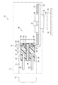
【解決手段】 光ファイバ保持孔20を有する光フェルール12と、光フェルール12の一端に備えた位置決め手段21を介して位置決めされて貼付けされたフレキシブル回路体14と、フレキシブル回路体14上において電子部品15に接続された受発光素子16と、を備え、光フェルール12に同一の端面を有するように研磨されて光ファイバ保持孔20に保持され、光接続可能な短尺光ファイバ13を備える光モジュール10。
【選択図】 図1
Description
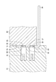
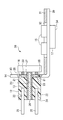
12 光フェルール
13 短尺光ファイバ
14 フレキシブル回路体
15 電子部品
16 受発光素子
20 光ファイバ保持孔
21 突起(位置決め手段)
22 ガイドピン孔
25 ガイドピン
27 光ファイバ挿通孔
28 位置決め孔(位置決め手段)
Claims (5)
- 光ファイバ保持孔を有する光フェルールと、
前記光フェルールの一端に配されたフレキシブル回路体と、
前記フレキシブル回路体上の電気回路に接続された光素子と、
前記光フェルールの他端に同一の端面を有するように前記光ファイバ保持孔に保持され、光接続可能な短尺光ファイバと、を備えることを特徴とする光モジュール。 - 前記短尺光ファイバは、前記光フェルールの一端から突出されて端面が前記光素子と対面するように保持され、
前記フレキシブル回路体は、前記フェルールの一端から突出した前記短尺光ファイバを挿通させる光ファイバ挿通孔を有することを特徴とする請求項1に記載した光モジュール。 - 前記光フェルールは、光接続される他端側に、光接続用のガイドピンを保持するためのガイドピン孔を有することを特徴とする請求項1又は請求項2に記載した光モジュール。
- 前記光フェルールは、突起が設けられ、
前記突起は前記フレキシブル回路体に設けられた位置決め孔と係合されていることを特徴とする請求項1乃至請求項3のいずれか一項に記載した光モジュール。 - 金型内にフレキシブル回路体と位置決めして光フェルールをインサート成形する工程と、
前記フレキシブル回路体上の電気回路に光素子を接続する工程と、
前記光フェルールに設けられているファイバ保持孔に短尺光ファイバを挿入して固定する工程と、
前記光フェルールの他端を前記短尺光ファイバと同一の端面を有するように研磨する工程と、を含むことを特徴とする光モジュールの製造方法。
Priority Applications (3)
| Application Number | Priority Date | Filing Date | Title |
|---|---|---|---|
| JP2007268924A JP4957503B2 (ja) | 2007-10-16 | 2007-10-16 | 光モジュールおよび光モジュールの製造方法 |
| US12/247,648 US7665905B2 (en) | 2007-10-16 | 2008-10-08 | Optical module and method for making the same |
| CN200810170248.7A CN101414032B (zh) | 2007-10-16 | 2008-10-16 | 光学模块及其制造方法 |
Applications Claiming Priority (1)
| Application Number | Priority Date | Filing Date | Title |
|---|---|---|---|
| JP2007268924A JP4957503B2 (ja) | 2007-10-16 | 2007-10-16 | 光モジュールおよび光モジュールの製造方法 |
Publications (2)
| Publication Number | Publication Date |
|---|---|
| JP2009098343A true JP2009098343A (ja) | 2009-05-07 |
| JP4957503B2 JP4957503B2 (ja) | 2012-06-20 |
Family
ID=40534294
Family Applications (1)
| Application Number | Title | Priority Date | Filing Date |
|---|---|---|---|
| JP2007268924A Active JP4957503B2 (ja) | 2007-10-16 | 2007-10-16 | 光モジュールおよび光モジュールの製造方法 |
Country Status (3)
| Country | Link |
|---|---|
| US (1) | US7665905B2 (ja) |
| JP (1) | JP4957503B2 (ja) |
| CN (1) | CN101414032B (ja) |
Cited By (8)
| Publication number | Priority date | Publication date | Assignee | Title |
|---|---|---|---|---|
| JP2012208146A (ja) * | 2011-03-29 | 2012-10-25 | Sumitomo Electric Ind Ltd | 光学モジュールの製造方法 |
| JP2012208305A (ja) * | 2011-03-29 | 2012-10-25 | Nitto Denko Corp | 光電気混載基板およびその製法 |
| WO2013065584A1 (ja) * | 2011-10-31 | 2013-05-10 | 山一電機株式会社 | 光モジュール |
| KR101327989B1 (ko) * | 2012-06-07 | 2013-11-13 | 주식회사 옵토웰 | 광송수신 모듈 제조방법 |
| JP2014089395A (ja) * | 2012-10-31 | 2014-05-15 | Kyocera Corp | 光装置用基板および光装置 |
| WO2014112461A1 (ja) | 2013-01-18 | 2014-07-24 | オリンパス株式会社 | 光伝送モジュールおよび撮像装置 |
| WO2025070309A1 (ja) * | 2023-09-29 | 2025-04-03 | 慶應義塾 | 一括成型マルチ光伝送シートアセンブリの製造方法 |
| WO2025070310A1 (ja) * | 2023-09-29 | 2025-04-03 | 慶應義塾 | 一括成型マルチ光伝送シートアセンブリの製造方法 |
Families Citing this family (21)
| Publication number | Priority date | Publication date | Assignee | Title |
|---|---|---|---|---|
| US8235603B2 (en) * | 2008-03-26 | 2012-08-07 | Sumitomo Electric Industries, Ltd. | Optoelectric conversion module, method for assembling same, and optoelectric information processor using same |
| TW201136077A (en) * | 2010-04-01 | 2011-10-16 | Hon Hai Prec Ind Co Ltd | Device and method for manufacturing optical couple connetor |
| JP5530332B2 (ja) * | 2010-10-27 | 2014-06-25 | 日本航空電子工業株式会社 | 光モジュール |
| US9323014B2 (en) * | 2012-05-28 | 2016-04-26 | Mellanox Technologies Ltd. | High-speed optical module with flexible printed circuit board |
| US9039302B2 (en) | 2012-06-15 | 2015-05-26 | Tyco Electronics Corporation | Interposer |
| US8821040B2 (en) * | 2012-06-15 | 2014-09-02 | Tyco Electronics Corporation | Interposer |
| JP5737254B2 (ja) * | 2012-09-26 | 2015-06-17 | 日立金属株式会社 | 光通信モジュール |
| TWI560481B (en) * | 2012-10-29 | 2016-12-01 | Hon Hai Prec Ind Co Ltd | Photoelectric converting module |
| DE102013101267B4 (de) * | 2013-02-08 | 2020-01-16 | HARTING Electronics GmbH | Gerätebuchse |
| US9804348B2 (en) | 2013-07-04 | 2017-10-31 | Mellanox Technologies, Ltd. | Silicon photonics connector |
| US9682500B2 (en) * | 2013-09-30 | 2017-06-20 | Apple Inc. | Insert molded parts and methods for forming the same |
| DE112016004062B4 (de) * | 2015-09-08 | 2023-11-02 | Vitesco Technologies GmbH | Verfahren zur Herstellung einer elektrooptischen Schnittstelle, elektrooptische Schnittstelle und Steuergerät |
| CN111736278A (zh) * | 2016-04-28 | 2020-10-02 | 苏州旭创科技有限公司 | 光模块 |
| US10608357B2 (en) | 2017-09-25 | 2020-03-31 | Molex, Llc | Electrical connection device |
| CN109560408B (zh) * | 2017-09-25 | 2020-08-25 | 美国莫列斯有限公司 | 电连接装置 |
| US12474529B2 (en) * | 2019-06-24 | 2025-11-18 | Te Connectivity Solutions Gmbh | Interposer |
| US12204149B2 (en) | 2019-06-24 | 2025-01-21 | Te Connectivity Solutions Gmbh | Interposer with feedback |
| EP3901677A1 (en) * | 2020-04-21 | 2021-10-27 | Koninklijke Philips N.V. | Optical transmission of signals to or from an electronic element |
| CN113970815B (zh) * | 2020-07-22 | 2022-11-08 | 青岛海信宽带多媒体技术有限公司 | 一种光模块 |
| US12360323B2 (en) | 2022-10-18 | 2025-07-15 | Mellanox Technologies, Ltd | Mechanical thermal interface for improved heat dissipation in network transceivers |
| US12242116B2 (en) * | 2023-07-10 | 2025-03-04 | Twinstar Technologies Co. Ltd. | Optical fiber connector device and method |
Citations (7)
| Publication number | Priority date | Publication date | Assignee | Title |
|---|---|---|---|---|
| WO2000013053A1 (fr) * | 1998-08-28 | 2000-03-09 | Fujikura Ltd. | Procede de montage d'un module optique et d'un element optique, et module optique avec receptacle |
| JP2000206376A (ja) * | 1999-01-08 | 2000-07-28 | Furukawa Electric Co Ltd:The | 受発光素子モジュ―ルおよびその作製方法 |
| JP2004317926A (ja) * | 2003-04-18 | 2004-11-11 | Nippon Telegr & Teleph Corp <Ntt> | 光コネクタ及びその組立方法 |
| JP2005062842A (ja) * | 2003-07-31 | 2005-03-10 | Toshiba Discrete Technology Kk | 光伝送デバイス |
| WO2005057262A1 (ja) * | 2003-12-15 | 2005-06-23 | Nec Corporation | 光モジュールおよびその製造方法 |
| JP2005340170A (ja) * | 2005-03-04 | 2005-12-08 | Teikoku Tsushin Kogyo Co Ltd | フレキシブル基板内蔵の電子部品用ケース |
| JP2006047682A (ja) * | 2004-08-04 | 2006-02-16 | Fujitsu Ltd | 基板および光素子相互接続用基板 |
Family Cites Families (17)
| Publication number | Priority date | Publication date | Assignee | Title |
|---|---|---|---|---|
| US6203212B1 (en) * | 1998-08-24 | 2001-03-20 | Agilent Technologies, Inc. | Optical subassembly for use in fiber optic data transmission and reception |
| US20010030789A1 (en) * | 1999-05-27 | 2001-10-18 | Wenbin Jiang | Method and apparatus for fiber optic modules |
| US6952532B2 (en) * | 1999-05-27 | 2005-10-04 | Jds Uniphase Corporation | Method and apparatus for multiboard fiber optic modules and fiber optic module arrays |
| US20020030872A1 (en) * | 1999-05-27 | 2002-03-14 | Edwin Dair | Method and apparatus for multiboard fiber optic modules and fiber optic module arrays |
| US20020033979A1 (en) * | 1999-05-27 | 2002-03-21 | Edwin Dair | Method and apparatus for multiboard fiber optic modules and fiber optic module arrays |
| JP2002261265A (ja) * | 2001-03-06 | 2002-09-13 | Sumitomo Electric Ind Ltd | 光通信装置 |
| US6910812B2 (en) * | 2001-05-15 | 2005-06-28 | Peregrine Semiconductor Corporation | Small-scale optoelectronic package |
| US6536957B1 (en) * | 2001-08-14 | 2003-03-25 | Nokia Corporation | Integrated optical transceiver array |
| US6729771B2 (en) * | 2001-12-17 | 2004-05-04 | Stratos Lightwave, Inc. | Parallel optics subassembly having at least twelve lenses |
| JP2004086137A (ja) * | 2002-07-01 | 2004-03-18 | Seiko Epson Corp | 光トランシーバ及びその製造方法 |
| WO2004027482A1 (de) * | 2002-09-23 | 2004-04-01 | Huber+Suhner Ag | Anschlussvorrichtung zum lösbaren verbinden wenigstens eines lichtwellenleiters mit wenigstens einem optoelektronischen bauelement sowie verfahren zum montieren einer solchen anschlussvorrichtung |
| US7129722B1 (en) * | 2002-10-09 | 2006-10-31 | Cypress Semiconductor Corp. | Methods of improving reliability of an electro-optical module |
| US20040252951A1 (en) * | 2003-05-12 | 2004-12-16 | Seiko Epson Corporation | Optical module and manufacturing method of the same |
| JP3795877B2 (ja) * | 2003-07-28 | 2006-07-12 | 株式会社東芝 | 光半導体モジュール及びその製造方法 |
| JP4923402B2 (ja) * | 2004-11-19 | 2012-04-25 | 富士通株式会社 | 光モジュールおよび電気配線基板 |
| JP4631640B2 (ja) | 2005-09-27 | 2011-02-16 | 住友電気工業株式会社 | 光接続部品の製造方法及び光接続部品 |
| JP4763446B2 (ja) * | 2005-12-19 | 2011-08-31 | 住友電気工業株式会社 | 光接続部品の製造方法 |
-
2007
- 2007-10-16 JP JP2007268924A patent/JP4957503B2/ja active Active
-
2008
- 2008-10-08 US US12/247,648 patent/US7665905B2/en not_active Expired - Fee Related
- 2008-10-16 CN CN200810170248.7A patent/CN101414032B/zh not_active Expired - Fee Related
Patent Citations (7)
| Publication number | Priority date | Publication date | Assignee | Title |
|---|---|---|---|---|
| WO2000013053A1 (fr) * | 1998-08-28 | 2000-03-09 | Fujikura Ltd. | Procede de montage d'un module optique et d'un element optique, et module optique avec receptacle |
| JP2000206376A (ja) * | 1999-01-08 | 2000-07-28 | Furukawa Electric Co Ltd:The | 受発光素子モジュ―ルおよびその作製方法 |
| JP2004317926A (ja) * | 2003-04-18 | 2004-11-11 | Nippon Telegr & Teleph Corp <Ntt> | 光コネクタ及びその組立方法 |
| JP2005062842A (ja) * | 2003-07-31 | 2005-03-10 | Toshiba Discrete Technology Kk | 光伝送デバイス |
| WO2005057262A1 (ja) * | 2003-12-15 | 2005-06-23 | Nec Corporation | 光モジュールおよびその製造方法 |
| JP2006047682A (ja) * | 2004-08-04 | 2006-02-16 | Fujitsu Ltd | 基板および光素子相互接続用基板 |
| JP2005340170A (ja) * | 2005-03-04 | 2005-12-08 | Teikoku Tsushin Kogyo Co Ltd | フレキシブル基板内蔵の電子部品用ケース |
Cited By (12)
| Publication number | Priority date | Publication date | Assignee | Title |
|---|---|---|---|---|
| JP2012208146A (ja) * | 2011-03-29 | 2012-10-25 | Sumitomo Electric Ind Ltd | 光学モジュールの製造方法 |
| JP2012208305A (ja) * | 2011-03-29 | 2012-10-25 | Nitto Denko Corp | 光電気混載基板およびその製法 |
| US8837873B2 (en) | 2011-03-29 | 2014-09-16 | Nitto Denko Corporation | Opto-electric hybrid board and manufacturing method therefor |
| WO2013065584A1 (ja) * | 2011-10-31 | 2013-05-10 | 山一電機株式会社 | 光モジュール |
| US9325418B2 (en) | 2011-10-31 | 2016-04-26 | Mellanox Technologies, Ltd. | Optical module with flexible wiring board |
| KR101327989B1 (ko) * | 2012-06-07 | 2013-11-13 | 주식회사 옵토웰 | 광송수신 모듈 제조방법 |
| JP2014089395A (ja) * | 2012-10-31 | 2014-05-15 | Kyocera Corp | 光装置用基板および光装置 |
| WO2014112461A1 (ja) | 2013-01-18 | 2014-07-24 | オリンパス株式会社 | 光伝送モジュールおよび撮像装置 |
| JP2014137584A (ja) * | 2013-01-18 | 2014-07-28 | Olympus Corp | 光伝送モジュールおよび撮像装置 |
| US9762329B2 (en) | 2013-01-18 | 2017-09-12 | Olympus Corporation | Optical transmission module and imaging device |
| WO2025070309A1 (ja) * | 2023-09-29 | 2025-04-03 | 慶應義塾 | 一括成型マルチ光伝送シートアセンブリの製造方法 |
| WO2025070310A1 (ja) * | 2023-09-29 | 2025-04-03 | 慶應義塾 | 一括成型マルチ光伝送シートアセンブリの製造方法 |
Also Published As
| Publication number | Publication date |
|---|---|
| US7665905B2 (en) | 2010-02-23 |
| US20090097802A1 (en) | 2009-04-16 |
| JP4957503B2 (ja) | 2012-06-20 |
| CN101414032B (zh) | 2015-05-13 |
| CN101414032A (zh) | 2009-04-22 |
Similar Documents
| Publication | Publication Date | Title |
|---|---|---|
| JP4957503B2 (ja) | 光モジュールおよび光モジュールの製造方法 | |
| TWI521250B (zh) | 電氣至光學及光學至電氣轉換頭插頭 | |
| JP4690963B2 (ja) | 多チャンネル光モジュールの製造方法 | |
| CA2714696C (en) | Optical path change member and holding member body | |
| CN100566045C (zh) | 光电复合式连接器以及使用它的基板 | |
| KR100833556B1 (ko) | 광 커넥터 | |
| US7563036B2 (en) | Optical element module and method of assembling the optical element module | |
| US8608390B2 (en) | Optical communication module | |
| JP2006301610A (ja) | 光結合装置 | |
| JP2012194481A (ja) | 光コネクタ、光ファイバの実装方法、及び電子情報機器 | |
| JP6528783B2 (ja) | レセプタクル、コネクタセット及びレセプタクルの製造方法 | |
| CN102455469B (zh) | 光模块 | |
| JP2009122354A (ja) | 光学ブロック補強材及び光学ブロック、並びにそれらを用いた光モジュール | |
| EP1909127A2 (en) | Lens and Tube Body Constituting an Element of an Optical Communication Module | |
| JP6460130B2 (ja) | コネクタ及びコネクタセット | |
| JP2009053280A (ja) | 光モジュール | |
| JP3926722B2 (ja) | 一芯双方向光送受信コネクタ | |
| JP2001518636A (ja) | オプトエレクトロニックなプラグ受容エレメントを製作する方法及びオプトエレクトロニックなプラグ | |
| JP2009229601A (ja) | 光モジュール | |
| JP2013218119A (ja) | 光接続部材及び光モジュール | |
| JP5892292B2 (ja) | 光プラグ及び光コネクタ | |
| JP2014178598A (ja) | 光素子モジュール | |
| JP2005233995A (ja) | 光電変換プラグの製造方法 | |
| JP4175288B2 (ja) | 光コネクタの製造方法 | |
| JP2011090148A (ja) | 光電気変換部品及びその製造方法 |
Legal Events
| Date | Code | Title | Description |
|---|---|---|---|
| A621 | Written request for application examination |
Free format text: JAPANESE INTERMEDIATE CODE: A621 Effective date: 20100715 |
|
| A977 | Report on retrieval |
Free format text: JAPANESE INTERMEDIATE CODE: A971007 Effective date: 20110803 |
|
| A131 | Notification of reasons for refusal |
Free format text: JAPANESE INTERMEDIATE CODE: A131 Effective date: 20110816 |
|
| A521 | Request for written amendment filed |
Free format text: JAPANESE INTERMEDIATE CODE: A523 Effective date: 20111012 |
|
| A131 | Notification of reasons for refusal |
Free format text: JAPANESE INTERMEDIATE CODE: A131 Effective date: 20111213 |
|
| A521 | Request for written amendment filed |
Free format text: JAPANESE INTERMEDIATE CODE: A523 Effective date: 20120127 |
|
| TRDD | Decision of grant or rejection written | ||
| A01 | Written decision to grant a patent or to grant a registration (utility model) |
Free format text: JAPANESE INTERMEDIATE CODE: A01 Effective date: 20120221 |
|
| A01 | Written decision to grant a patent or to grant a registration (utility model) |
Free format text: JAPANESE INTERMEDIATE CODE: A01 |
|
| A61 | First payment of annual fees (during grant procedure) |
Free format text: JAPANESE INTERMEDIATE CODE: A61 Effective date: 20120305 |
|
| FPAY | Renewal fee payment (event date is renewal date of database) |
Free format text: PAYMENT UNTIL: 20150330 Year of fee payment: 3 |
|
| R150 | Certificate of patent or registration of utility model |
Ref document number: 4957503 Country of ref document: JP Free format text: JAPANESE INTERMEDIATE CODE: R150 Free format text: JAPANESE INTERMEDIATE CODE: R150 |
|
| R250 | Receipt of annual fees |
Free format text: JAPANESE INTERMEDIATE CODE: R250 |
|
| R250 | Receipt of annual fees |
Free format text: JAPANESE INTERMEDIATE CODE: R250 |
|
| R250 | Receipt of annual fees |
Free format text: JAPANESE INTERMEDIATE CODE: R250 |
|
| R250 | Receipt of annual fees |
Free format text: JAPANESE INTERMEDIATE CODE: R250 |
|
| R250 | Receipt of annual fees |
Free format text: JAPANESE INTERMEDIATE CODE: R250 |
|
| R250 | Receipt of annual fees |
Free format text: JAPANESE INTERMEDIATE CODE: R250 |