JP2009123719A - Device mounting substrate, manufacturing method thereof, semiconductor module, and portable device - Google Patents
Device mounting substrate, manufacturing method thereof, semiconductor module, and portable device Download PDFInfo
- Publication number
- JP2009123719A JP2009123719A JP2007290839A JP2007290839A JP2009123719A JP 2009123719 A JP2009123719 A JP 2009123719A JP 2007290839 A JP2007290839 A JP 2007290839A JP 2007290839 A JP2007290839 A JP 2007290839A JP 2009123719 A JP2009123719 A JP 2009123719A
- Authority
- JP
- Japan
- Prior art keywords
- region
- wiring
- layer
- substrate
- element mounting
- Prior art date
- Legal status (The legal status is an assumption and is not a legal conclusion. Google has not performed a legal analysis and makes no representation as to the accuracy of the status listed.)
- Granted
Links
Images


Classifications
-
- H—ELECTRICITY
- H10—SEMICONDUCTOR DEVICES; ELECTRIC SOLID-STATE DEVICES NOT OTHERWISE PROVIDED FOR
- H10W—GENERIC PACKAGES, INTERCONNECTIONS, CONNECTORS OR OTHER CONSTRUCTIONAL DETAILS OF DEVICES COVERED BY CLASS H10
- H10W70/00—Package substrates; Interposers; Redistribution layers [RDL]
- H10W70/60—Insulating or insulated package substrates; Interposers; Redistribution layers
-
- H—ELECTRICITY
- H10—SEMICONDUCTOR DEVICES; ELECTRIC SOLID-STATE DEVICES NOT OTHERWISE PROVIDED FOR
- H10W—GENERIC PACKAGES, INTERCONNECTIONS, CONNECTORS OR OTHER CONSTRUCTIONAL DETAILS OF DEVICES COVERED BY CLASS H10
- H10W74/00—Encapsulations, e.g. protective coatings
- H10W74/10—Encapsulations, e.g. protective coatings characterised by their shape or disposition
- H10W74/15—Encapsulations, e.g. protective coatings characterised by their shape or disposition on active surfaces of flip-chip devices, e.g. underfills
Landscapes
- Internal Circuitry In Semiconductor Integrated Circuit Devices (AREA)
- Non-Metallic Protective Coatings For Printed Circuits (AREA)
- Structure Of Printed Boards (AREA)
- Manufacturing Of Printed Wiring (AREA)
Abstract
【課題】パッド電極部から浸入する水分が配線パターン表面を拡散するのを抑制し、半導体モジュールの信頼性を向上させる。
【解決手段】半導体モジュールの配線パターン2は、絶縁基板1上に形成され、配線領域4aと、半導体素子との接続を行う電極領域4cと、配線領域4aと電極領域4cとの間に設けた境界領域4bとから構成される。配線パターン2の電極領域4cにはその表面に金めっき層5が設けられる。境界領域4bにおける配線パターン2の上面は配線領域4aにおける配線パターン2の上面よりも窪むように形成され、境界領域4bには段差部2bが設けられる。ソルダーレジスト6は、金めっき層5の一部、及び境界領域4bと配線領域4aの配線パターンを被覆して形成され、半導体素子との接続を行うための所定の開口部6aを有する。電極領域4cにおける金めっき層5には導電部材8が接続され、封止樹脂層12がこれら全体を封止している。
【選択図】図2[PROBLEMS] To suppress the diffusion of moisture entering from a pad electrode portion on the surface of a wiring pattern and improve the reliability of a semiconductor module.
A wiring pattern 2 of a semiconductor module is formed on an insulating substrate 1 and provided between a wiring region 4a, an electrode region 4c for connection with a semiconductor element, and between the wiring region 4a and the electrode region 4c. The boundary region 4b. A gold plating layer 5 is provided on the surface of the electrode region 4 c of the wiring pattern 2. The upper surface of the wiring pattern 2 in the boundary region 4b is formed so as to be recessed from the upper surface of the wiring pattern 2 in the wiring region 4a, and a step 2b is provided in the boundary region 4b. The solder resist 6 is formed so as to cover a part of the gold plating layer 5 and the wiring pattern of the boundary region 4b and the wiring region 4a, and has a predetermined opening 6a for connection with a semiconductor element. A conductive member 8 is connected to the gold plating layer 5 in the electrode region 4c, and a sealing resin layer 12 seals the whole.
[Selection] Figure 2
Description
本発明は、素子搭載用基板に関し、特にパッド電極を備える素子搭載用基板に関する。 The present invention relates to an element mounting substrate, and more particularly to an element mounting substrate including a pad electrode.
携帯電話、PDA、DVC、DSCといったポータブルエレクトロニクス機器の高機能化が加速するなか、こうした製品が市場で受け入れられるためには小型・軽量化が必須となっており、その実現のために高集積のシステムLSIが求められている。一方、これらのエレクトロニクス機器に対しては、より使い易く便利なものが求められており、機器に使用されるLSIに対し、高機能化、高性能化が要求されている。このため、LSIチップの高集積化にともないそのI/O数が増大する一方でパッケージ自体の小型化要求も強く、これらを両立させるために、半導体部品の高密度な基板実装に適合した半導体パッケージの開発が強く求められている。こうした要求に対応するため、CSP(Chip Size Package)と呼ばれるパッケージ技術が種々開発されている。 As portable electronics devices such as mobile phones, PDAs, DVCs, and DSCs are accelerating their functions, miniaturization and weight reduction are essential for these products to be accepted in the market. There is a need for a system LSI. On the other hand, these electronic devices are required to be easier to use and convenient, and higher functionality and higher performance are required for LSIs used in the devices. For this reason, as the number of I / Os increases with higher integration of LSI chips, there is a strong demand for miniaturization of the package itself. In order to achieve both of these, a semiconductor package suitable for high-density board mounting of semiconductor components Development is strongly demanded. In order to meet such demands, various package technologies called CSP (Chip Size Package) have been developed.
こうしたパッケージの例として、BGA(Ball Grid Array)が知られている。BGA
は、パッケージ用基板の上に半導体チップを実装し、それを樹脂モールディングした後、反対側の面に外部端子としてハンダボールをエリア状に形成したものである。
As an example of such a package, BGA (Ball Grid Array) is known. BGA
In this example, a semiconductor chip is mounted on a package substrate, resin-molded, and then solder balls are formed in an area as external terminals on the opposite surface.
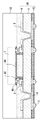
図13は特許文献1に記載されたBGA型の半導体モジュールの概略断面図である。この半導体装置は、回路基板110の一方の面に半導体素子106を搭載し、他方の面に外部接続端子としてはんだボール112を接合したものである。回路基板110の一方の面には半導体素子106と電気的に接続する配線パターン103(パッド電極部103a)が設けられ、回路基板110の他方の面には外部接続端子を接合するランド部103bが設けられている。配線パターン103とランド部103bとの電気的接続は絶縁基板101を貫通する貫通孔111の内壁面に設けた導体部を介してなされる。ソルダーレジスト105は回路基板110の表面を保護している。回路基板110の一方の面は半導体素子106を搭載した後、封止樹脂層108により封止されている。
FIG. 13 is a schematic cross-sectional view of a BGA type semiconductor module described in
図14は図13に示した半導体装置のパッド電極部(図13のXで示した断面部分)を拡大した断面図である。半導体素子106と金線などのワイヤ107によりワイヤ接続されるパッド電極部103aは、銅からなる配線部と、その表面を覆う金めっき層104から構成されている。ソルダーレジスト105は、パッド電極部103aにおける銅配線部を被覆し、さらに金めっき層104の一部を被覆するように設けられている。ソルダーレジスト105の開口部は、半導体素子106の搭載およびワイヤ接続などがなされた後、封止樹脂層108によって半導体素子106とともに封止される。
しかしながら、ソルダーレジスト105や封止樹脂層108は外部からの水分がこれら自体を浸透するのを抑制しているものの、それぞれの界面を経由する水分の浸入を抑制することはできていない。特に金めっき層104の表面は平滑であるため、ソルダーレジスト105との界面を経由して配線パターン103側に水分が入り込みやすい構造となっている。このため、金めっき層104近傍の配線パターン103部分には水分が多く存在する。このように入り込んだ水分がさらに配線パターン103の表面上を拡散していった場合には、半導体モジュールの動作時にプラス電圧に印加されている配線パターン103部分から溶け出した銅イオンが絶縁基板101とソルダーレジスト105との界面を移動して、マイナス電圧が印加されている配線パターン103部分に析出し、いわゆるイオンマイグレーションによるショート(絶縁破壊)が発生するという問題がある。こうした問題は従来の半導体モジュールの信頼性を向上させるのに大きな障害となっている。
However, although the solder resist 105 and the sealing
本発明は上記事情に鑑みなされたものであって、その目的とするところは、パッド電極部から浸入する水分が配線パターン表面を拡散するのを抑制し、素子搭載用基板の信頼性を向上させることにある。 The present invention has been made in view of the above circumstances, and an object of the present invention is to prevent moisture entering from the pad electrode portion from diffusing on the surface of the wiring pattern and to improve the reliability of the element mounting substrate. There is.
本発明のある態様は、素子搭載用基板である。当該素子搭載用基板は、配線領域とこれに接続された電極領域を含み、配線領域と電極領域との境界領域に段差部を有する、銅からなる配線層と、電極領域における配線層の表面に形成された金めっき層と、金めっき層の一部と、境界領域および配線領域の配線層とを被覆して形成され、電極領域に所定の開口部を有する絶縁層と、を備えることを特徴とする。ここで、電極領域の電極とは、たとえば、パッケージ基板もしくはモジュール基板などの回路基板に設けられたパッド電極、あるいはLSIチップに代表される半導体素子に設けられたパッド電極を意味する。この電極により、素子搭載用基板とLSIチップに代表される半導体素子とをワイヤボンディングで接続したり、素子搭載用基板と外部の半導体装置とをワイヤボンディングで接続したりする。 One embodiment of the present invention is an element mounting substrate. The element mounting substrate includes a wiring layer made of copper, including a wiring region and an electrode region connected thereto, and having a step portion at a boundary region between the wiring region and the electrode region, and a surface of the wiring layer in the electrode region. A gold plating layer formed, a part of the gold plating layer, an insulating layer formed so as to cover the boundary region and the wiring layer in the wiring region, and having a predetermined opening in the electrode region, And Here, the electrode in the electrode region means, for example, a pad electrode provided on a circuit board such as a package substrate or a module substrate, or a pad electrode provided on a semiconductor element typified by an LSI chip. With this electrode, the element mounting substrate and a semiconductor element typified by an LSI chip are connected by wire bonding, or the element mounting substrate and an external semiconductor device are connected by wire bonding.
この態様によれば、金めっき層と絶縁層の界面を介して浸入する水分が配線層の表面上を拡散していく距離に関して、その拡散距離が従来のように段差部を設けない場合に比べて長くなる。このため、配線領域における配線層への水分の供給が抑制され、配線層間でイオンマイグレーションが発生しにくくなる。この結果、素子搭載用基板の信頼性を向上させることができる。 According to this aspect, with respect to the distance that moisture that penetrates through the interface between the gold plating layer and the insulating layer diffuses on the surface of the wiring layer, the diffusion distance is smaller than that in the case where the step portion is not provided as in the prior art. Become longer. For this reason, the supply of moisture to the wiring layer in the wiring region is suppressed, and ion migration hardly occurs between the wiring layers. As a result, the reliability of the element mounting substrate can be improved.
上記態様において、段差部は配線領域の配線層の上面よりも窪んで形成されていることが好ましい。このようにすることで、段差部の底部側に水分が留まりやすくなり、段差部が浸入した水分の障壁として作用するため、配線層の境界領域から配線領域への水分の拡散がさらに抑制される。この結果、素子搭載用基板の信頼性をさらに向上させることができる。 In the above aspect, the stepped portion is preferably formed to be recessed from the upper surface of the wiring layer in the wiring region. By doing so, it becomes easier for moisture to stay on the bottom side of the stepped portion, and the stepped portion acts as a barrier to the infiltrated moisture, so that the diffusion of moisture from the boundary region of the wiring layer to the wiring region is further suppressed. . As a result, the reliability of the element mounting substrate can be further improved.
上記態様において、境界領域において絶縁層と接する配線層の表面は粗面加工が施されていることが好ましい。この場合、境界領域における配線層の表面に微細な凹凸が設けられるので、浸入する水分の配線層の表面上の拡散距離が長くなりその拡散が制限される。また、配線層の表面に微細な凹凸が設けられると、その部分では絶縁層との密着性が向上するので、浸入する水分が境界領域における配線層と絶縁層との界面をより拡散しにくくなる。これらの結果、配線層の境界領域から配線領域への水分の拡散がさらに抑制され、素子搭載用基板の信頼性をさらに向上させることができる。 In the above aspect, the surface of the wiring layer in contact with the insulating layer in the boundary region is preferably roughened. In this case, since fine irregularities are provided on the surface of the wiring layer in the boundary region, the diffusion distance on the surface of the wiring layer of the invading moisture becomes long and the diffusion is limited. In addition, when fine irregularities are provided on the surface of the wiring layer, the adhesiveness with the insulating layer is improved at that portion, so that the intruding moisture is less likely to diffuse at the interface between the wiring layer and the insulating layer in the boundary region. . As a result, the diffusion of moisture from the boundary region of the wiring layer to the wiring region is further suppressed, and the reliability of the element mounting substrate can be further improved.
上記態様において、配線層および絶縁層は基板上に設けられ、配線層は基板と接する側の縁部に沿って基板との間に隙間を有し、絶縁層はこの隙間を埋め込むように形成されていてもよい。このようにすることで、隙間に埋め込まれた絶縁層のアンカー効果により配線層と絶縁層との密着性が向上するので、浸入する水分が配線領域における配線層の表面上をより拡散しにくくなる。この結果、素子搭載用基板の信頼性をさらに向上させることができる。 In the above aspect, the wiring layer and the insulating layer are provided on the substrate, the wiring layer has a gap between the substrate and the edge along the side in contact with the substrate, and the insulating layer is formed so as to fill the gap. It may be. By doing so, the anchoring effect of the insulating layer embedded in the gap improves the adhesion between the wiring layer and the insulating layer, so that the intruding moisture is less likely to diffuse on the surface of the wiring layer in the wiring region. . As a result, the reliability of the element mounting substrate can be further improved.
本発明の他の態様は、半導体モジュールである。当該半導体モジュールは、上述したいずれかの態様の素子搭載用基板と、当該素子搭載用基板に実装された半導体素子と、を備えることを特徴とする。この態様において、半導体素子が素子搭載用基板にワイヤボンディング接続されていてもよい。また、半導体素子が素子搭載用基板にフリップチップ接続されていてもよい。 Another embodiment of the present invention is a semiconductor module. The semiconductor module includes the element mounting substrate according to any one of the aspects described above and a semiconductor element mounted on the element mounting substrate. In this aspect, the semiconductor element may be connected to the element mounting substrate by wire bonding. Further, the semiconductor element may be flip-chip connected to the element mounting substrate.
本発明のさらに他の態様は携帯機器である。当該携帯機器は、上述したいずれかの態様の半導体モジュールを搭載したことを特徴とする。 Yet another embodiment of the present invention is a portable device. The portable device is characterized in that the semiconductor module according to any one of the above-described aspects is mounted.
本発明のさらに他の態様は、素子搭載用基板の製造方法である。当該素子搭載用基板の製造方法は、基板の上に第1の金属層を形成する工程と、第1の金属層をパターニングして、電極領域、配線領域、および電極領域と配線領域の間に設けられた境界領域を有する配線を形成する工程と、配線および基板の表面に第2の金属層を形成する工程と、電極領域、境界領域、ならびに電極領域および境界領域の周囲の所定領域において第2の金属層の一部が露出するように、基板の上に第1のマスクを形成する工程と、第1のマスクを用いて、電極領域、境界領域、ならびに電極領域および境界領域の周囲の所定領域の第2の金属層を選択的に除去した後、電極領域および境界領域の配線層を掘り下げて、境界領域の表面を配線領域の表面より低くする工程と、第1のマスクを除去する工程と、電極領域の配線および電極領域の周囲の所定領域の基板が露出するように、基板の上に第2のマスクを形成する工程と、第2の金属層をめっきリードとして用いて電極領域に金めっき層を形成する工程と、第2のマスクおよび第2の金属層を除去する工程と、電極領域の一部、境界領域および配線領域の配線層とを絶縁層で被覆する工程と、を備えることを特徴とする。 Yet another embodiment of the present invention is a method for manufacturing an element mounting substrate. The element mounting substrate manufacturing method includes the steps of forming a first metal layer on the substrate, patterning the first metal layer, and interposing the electrode region, the wiring region, and the electrode region and the wiring region. A step of forming a wiring having the provided boundary region, a step of forming a second metal layer on the surface of the wiring and the substrate, and the electrode region, the boundary region, and the electrode region and the predetermined region around the boundary region. Forming a first mask on the substrate so that a part of the metal layer of the two is exposed, and using the first mask, the electrode region, the boundary region, and the periphery of the electrode region and the boundary region After selectively removing the second metal layer in the predetermined region, the step of digging down the electrode layer and the wiring layer in the boundary region to lower the surface of the boundary region below the surface of the wiring region, and removing the first mask Process and electrode area wiring And forming a second mask on the substrate so that the substrate in a predetermined region around the electrode region is exposed, and forming a gold plating layer in the electrode region using the second metal layer as a plating lead And a step of removing the second mask and the second metal layer, and a step of covering a part of the electrode region, the boundary region, and the wiring layer of the wiring region with an insulating layer. .
上記態様の素子搭載用基板製造方法において、第1の金属層を無電解めっき、および電解めっきを用いて形成してもよい。また、第2の金属層を無電解めっきを用いて形成してもよい。また、金めっき層がAu/Ni層、またはAu/Pd/Ni層であってもよい。 In the element mounting substrate manufacturing method of the above aspect, the first metal layer may be formed using electroless plating and electrolytic plating. Further, the second metal layer may be formed using electroless plating. Further, the gold plating layer may be an Au / Ni layer or an Au / Pd / Ni layer.
また、上記態様の素子搭載用基板製造方法において、配線を形成した後、配線の表面を粗化させる工程を、さらに備えてもよい。 The element mounting substrate manufacturing method of the above aspect may further include a step of roughening the surface of the wiring after the wiring is formed.
また、上記態様の素子搭載用基板製造方法において、絶縁層が被覆される領域にある配線の底部の縁部に沿って、当該配線と基板との間に隙間を設けた後、絶縁層を形成してもよい。 Further, in the element mounting substrate manufacturing method according to the above aspect, the insulating layer is formed after providing a gap between the wiring and the substrate along the edge of the bottom of the wiring in the region covered with the insulating layer. May be.
本発明によれば、パッド電極部から浸入する水分が配線パターン表面を拡散するのを抑制し、素子搭載用基板の信頼性を向上させることができる。 ADVANTAGE OF THE INVENTION According to this invention, it can suppress that the water | moisture content permeate | transmitted from a pad electrode part diffuses the wiring pattern surface, and can improve the reliability of an element mounting board | substrate.
以下、本発明を具現化した実施形態について図面に基づいて説明する。なお、すべての図面において、同様な構成要素には同様の符号を付し、適宜説明を省略する。 DESCRIPTION OF EXEMPLARY EMBODIMENTS Hereinafter, embodiments of the invention will be described with reference to the drawings. In all the drawings, the same reference numerals are given to the same components, and the description will be omitted as appropriate.
(第1実施形態)
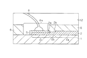
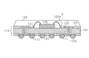
図1は第1実施形態に係るパッド電極を備えた半導体モジュールの概略断面図である。また、図2は図1に示した半導体モジュールのパッド電極部(図1のXで示した断面部分)を拡大した断面図であり、図3は図1に示した半導体モジュールのパッド電極部を上面側からみた概略平面図である。なお、図2は図3中のA−A線に沿った断面図である。
(First embodiment)
FIG. 1 is a schematic cross-sectional view of a semiconductor module including a pad electrode according to the first embodiment. 2 is an enlarged cross-sectional view of the pad electrode portion (cross-sectional portion indicated by X in FIG. 1) of the semiconductor module shown in FIG. 1, and FIG. 3 shows the pad electrode portion of the semiconductor module shown in FIG. It is the schematic plan view seen from the upper surface side. 2 is a cross-sectional view taken along the line AA in FIG.
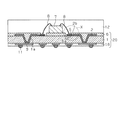
第1実施形態の半導体モジュールは、素子搭載用基板20の上面に半導体素子7を搭載し、下面に外部接続端子としてはんだボール11を接合したものである。素子搭載用基板20の上面には半導体素子7と電気的に接続する銅からなる配線パターン2が設けられ、素子搭載用基板20の下面には外部接続端子を接合する銅からなる配線パターン9が設けられている。配線パターン2と配線パターン9との電気的接続は絶縁基板1を貫通するビアホール1aの内壁面に設けた導体部を介してなされる。配線パターン2はその表面に金めっき層5が設けられた電極領域4cと段差部2bを有し、電極領域4cにおいて導電部材8を介して半導体素子7と接続されている。ソルダーレジスト6およびソルダーレジスト10は配線パターン2および配線パターン9の表面をそれぞれ保護している。さらに、素子搭載用基板20の上面、および素子搭載用基板20に搭載された半導体素子7は、封止樹脂層12により封止されている。
In the semiconductor module of the first embodiment, the
具体的には、図2に示すように、配線パターン2は、コア基材として機能する絶縁基板1上に形成され、回路配線の引き回しや上下配線間の接続などを行う配線領域4aと、半導体素子7との接続を行う電極領域(パッド電極部)4cと、配線領域4aと電極領域4cとの間に設けられた境界領域4bとから構成されている。配線パターン2の電極領域4cにはその表面に金めっき層5が設けられている。境界領域4bにおける配線パターンの上面は配線領域4aにおける配線パターンの上面よりも窪むように形成され、境界領域4bには段差部2bが設けられている。この段差部2bは、図3に示すように、配線パターン2を横断するように設けられている。ソルダーレジスト6は、金めっき層5の一部、及び境界領域4bと配線領域4aの配線パターンを被覆して形成され、半導体素子7との接続を行うための所定の開口部6aを有している。電極領域4cにおける金めっき層5には導電部材8が接続され、封止樹脂層12がこれら全体を封止している。
Specifically, as shown in FIG. 2, the
なお、配線パターン2は「配線層」、配線領域4aは「配線領域」、境界領域4bは「境界領域」、電極領域4cは「電極領域」、金めっき層5は「金めっき層」、ソルダーレジスト6は「絶縁層」、及び段差部2bは「段差部」の一例である。
The
(製造方法)
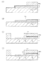
図4〜図6は、図2に示した素子搭載用基板に係るパッド電極部の製造プロセスを説明するための概略断面図である。次に、図2、図4〜図6を参照して、第1実施形態による素子搭載用基板のパッド電極部の製造プロセスについて説明する。
(Production method)
4 to 6 are schematic cross-sectional views for explaining the manufacturing process of the pad electrode portion according to the element mounting substrate shown in FIG. Next, with reference to FIGS. 2 and 4 to 6, a process for manufacturing the pad electrode portion of the element mounting substrate according to the first embodiment will be described.
まず、図4(A)に示すように、コア基材として機能する絶縁基板1上に、無電界めっき法および電界めっき法を用いて銅からなる配線層2zを約20μmの厚みで形成する。
First, as shown in FIG. 4A, a
絶縁基板1にはエポキシ樹脂を主成分とする膜が採用され、その厚さは、たとえば、約100μmである。素子搭載用基板の放熱性向上の観点から、絶縁基板1は高熱伝導性を有することが望ましい。このため、絶縁基板1は、銀、ビスマス、銅、アルミニウム、マグネシウム、錫、亜鉛およびこれらの合金などやシリカ、アルミナ、窒化ケイ素、窒化アルミニウムなどを高熱伝導性フィラーとして含有することが好ましい。なお、本実施形態では、図1に示したように、絶縁基板1にはビアホール1aを設けているが、本製造方法での説明では省略する。
The insulating
図4(B)に示すように、フォトリソグラフィ技術を用いて配線層2z上に所定のパターンを有するレジストマスクPR1を形成する。
As shown in FIG. 4B, a resist mask PR1 having a predetermined pattern is formed on the
図4(C)に示すように、塩化第二鉄を使用したウェットエッチング技術を用いて配線層2zをパターニングした後、ウェット処理によりレジストマスクPR1を除去する。その後、薬液による洗浄処理を行うことでアッシング時に発生する残渣などを剥離する。これにより、所定の回路配線を有する配線パターン2が形成される。
As shown in FIG. 4C, after patterning the
図4(D)に示すように、無電解めっき法を用いて配線パターン2を含む絶縁基板1上の全面に銅薄膜3zを約1μmの厚みでめっきする。
As shown in FIG. 4D, a copper
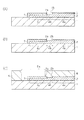
次に、図5(A)に示すように、フォトリソグラフィ技術を用いて銅薄膜3z上に所定のパターンを有するレジストマスクPR2を形成する。この際、レジストマスクPR2は電極領域4cおよび境界領域4bにおける銅薄膜3z上には形成しないようにする。
Next, as shown in FIG. 5A, a resist mask PR2 having a predetermined pattern is formed on the copper
図5(B)に示すように、エッチング技術を用いて銅薄膜3zをパターニングした後、ウェット処理によりレジストマスクPR2を剥離する。この際、境界領域4bにおける配線パターン2の表面も同時にエッチングされるため、境界領域4bにおける配線パターン2の上面は配線領域4aにおける配線パターン2の上面よりも窪み、境界領域4bには銅薄膜3の厚さに対応した段差部2b(段差約1μm)が形成される。これにより、後の工程で金めっき層5をめっき形成する際に、配線パターン2に対して一括して給電するための銅薄膜3が形成される。言い換えると、銅薄膜3は、金めっき層5を形成する際のめっきリードとして用いられる。
As shown in FIG. 5B, after patterning the copper
図5(C)に示すように、フォトリソグラフィ技術を用いて配線パターン2における電極領域4cを含む部分に開口部を有する耐金レジストマスクPR3を形成する。この際、境界領域4bは耐金レジストマスクPR3によって覆われている。
As shown in FIG. 5C, a gold-resistant resist mask PR3 having an opening in a portion including the
図5(D)に示すように、エッチング技術を用いて銅薄膜3の表面を約5μm程度ソフトエッチングし、段差部2aを形成する。これにより、後の工程で金めっき層5を形成した際に、パッド電極部(電極領域4c)における配線の厚み(高さ)を低減することが可能になる。
As shown in FIG. 5D, the surface of the copper
次に、図6(A)に示すように、選択めっき法を用いて、所定領域(電極領域4c)における配線パターン2の表面に金めっき層(電解Au/Niめっき膜)5を約5.5μm(約0.5μm/約5μm)の厚みで形成する。その後、ウェット処理により耐金レジストマスクPR3を剥離する。これにより、配線パターン2の電極領域4cの表面に金めっき層5が選択的に形成される。なお、金めっき層5は、Au/Ni層に限られず、たとえば、金めっき層5としてAu/Pb/Ni層を用いてもよい。
Next, as shown in FIG. 6A, a gold plating layer (electrolytic Au / Ni plating film) 5 is formed on the surface of the
図6(B)に示すように、エッチング技術を用いて全面エッチングすることにより銅薄膜3を除去する。
As shown in FIG. 6B, the copper
図6(C)に示すように、所定の開口部6aを有し、金めっき層5の一部と、境界領域4bおよび配線領域4aの配線パターン2とを被覆するようにソルダーレジスト6を形成する。ソルダーレジスト6は配線パターン2の保護膜として機能する。
As shown in FIG. 6C, a solder resist 6 is formed so as to have a
最後に、図1に示したように、配線パターン2の電極領域4cにおける金めっき層5に
導電部材8をワイヤボンディング接続する。ここで、導電部材8には金線などが採用される。その後、これら全体を封止するための封止樹脂層12を形成する。封止樹脂層12は、ソルダーレジスト6の上に形成され、半導体素子7(図1参照)および配線パターン2の電極領域4c(金めっき層5)を覆うように全面に形成される。この封止樹脂層12は、半導体素子7を外界からの影響から保護している。封止樹脂層12の材料は、たとえば、エポキシ樹脂などの熱硬化性の絶縁性の樹脂である。なお、封止樹脂層12中には熱伝導性を高めるためのフィラーが添加されていてもよい。
Finally, as shown in FIG. 1, the
これらの工程により、第1実施形態の素子搭載用基板(素子搭載用基板のパッド電極部)を得ることができる。 Through these steps, the element mounting substrate of the first embodiment (pad electrode portion of the element mounting substrate) can be obtained.
以上説明した第1実施形態の素子搭載用基板および半導体モジュールによれば、以下のような効果を得ることができるようになる。
(1)金めっき層5との境界領域4bに段差部2bを設けたことで、金めっき層5とソルダーレジスト6の界面を介して浸入する水分が配線パターン2の表面上を拡散していく距離に関して、その拡散距離が従来のように段差部を設けない場合に比べて長くなる。このため、配線領域4aにおける配線パターン2への水分の供給(拡散)が抑制され、配線パターン間でイオンマイグレーションが発生しにくくなる。この結果、素子搭載用基板ひいては半導体モジュールの信頼性を向上させることができる。
(2)境界領域4bにおける配線パターン2の上面が配線領域4aにおける配線パターン2の上面よりも窪むように段差部2bを形成したことで、段差部2bの底部側に水分が留まりやすくなり、段差部2bが浸入した水分の障壁として作用するため、配線パターン2の境界領域4bから配線領域4aへの水分の拡散がさらに抑制される。この結果、素子搭載用基板ひいては半導体モジュールの信頼性をさらに向上させることができる。
(3)配線パターン2の表面に境界領域4bの段差部2bを含む凹状の窪みを設けたことで、ソルダーレジスト6との間にアンカー効果が生じ、配線パターン2とソルダーレジスト6との間の密着性が向上する。このため、浸入する水分が境界領域4bにおける配線パターン2の表面上をより拡散しにくくなる。この結果、素子搭載用基板ひいては半導体モジュールの信頼性をさらに向上させることができる。
(4)金めっき層5との境界領域4bに段差部2bを設けたことで、段差部2bが水分の浸入源に隣接して確実に水分の拡散を抑制するので、配線領域4a内に段差部が設けられている場合に比べて、素子搭載用基板ひいては半導体モジュールの信頼性をより効果的に向上させることができる。
According to the element mounting substrate and the semiconductor module of the first embodiment described above, the following effects can be obtained.
(1) By providing the
(2) Since the stepped
(3) By providing a concave depression including the stepped
(4) Since the stepped
(第2実施形態)
図7は図3中のB−B線に沿った断面図に相当し、図7(A)は第1実施形態に係る半導体モジュールの断面図であり、図7(B)は第2実施形態に係る半導体モジュールの断面図である。
(Second Embodiment)
7 corresponds to a cross-sectional view taken along line BB in FIG. 3, FIG. 7 (A) is a cross-sectional view of the semiconductor module according to the first embodiment, and FIG. 7 (B) is a second embodiment. It is sectional drawing of the semiconductor module which concerns on.
第1実施形態の半導体モジュールにおける配線パターン2は、図7(A)に示すように、絶縁基板1上に矩形の配線パターン2が形成され、これをソルダーレジスト6が被覆形成している。これに対して、第2実施形態の半導体モジュールにおける配線パターン2は、その底部が裾引き状態2cに広がり、さらにその部分の縁部に沿って絶縁基板1との間に隙間1bを有している。それ以外については、先の第1実施形態と同様である。
In the
このような半導体モジュールは、図4(C)に示した工程でのエッチング条件を制御して配線パターン2の形状をその底部が裾引き状態2cになるよう加工した上で、図4(C)、図5(B)、及び図6(A)に示した工程での薬液処理を制御して絶縁基板1を等方的にエッチングすることで、配線パターン2の底部の縁部に沿って絶縁基板1との間に隙間1bを形成することができる。なお、隙間1bは配線パターン2上にソルダーレジスト6を形成する際に、ソルダーレジスト6により容易に埋め込まれる。
In such a semiconductor module, the etching conditions in the step shown in FIG. 4C are controlled to process the shape of the
この第2実施形態の半導体モジュールによれば、上記(1)〜(4)の効果に加え、以下のよう
な効果を得ることができるようになる。
(5)配線パターン2に絶縁基板1と接する側の縁部に沿って絶縁基板1との間に隙間1bを設け、ソルダーレジスト6がこの隙間1bを埋め込むように形成したことで、隙間1bに埋め込まれたソルダーレジスト6のアンカー効果により配線パターン2とソルダーレジスト6との密着性が向上するので、浸入する水分が配線領域4aにおける配線パターン2の表面上をより拡散しにくくなる。この結果、半導体モジュールの信頼性をさらに向上させることができる。
(6)配線パターン2の底部を裾引き状態にし、その下部に隙間1bを設けたことで、配線パターン2の側面を絶縁基板1側に移動していく水分の拡散距離が、それらが設けられていない場合に比べて長くなるので、水分の供給が抑制され、その分、配線パターン間でイオンマイグレーションが発生しにくくなる。この結果、半導体モジュールの信頼性を向上する。
According to the semiconductor module of the second embodiment, the following effects can be obtained in addition to the effects (1) to (4).
(5) The gap 1b is provided between the
(6) Since the bottom portion of the
(第3実施形態)
図8は第3実施形態に係る半導体モジュールのパッド電極部の断面図である。第1実施形態と異なる箇所は、境界領域4bおよび配線領域4aにおける配線パターン2の表面が粗面加工が施されていることである。それ以外については、先の第1実施形態と同様である。
(Third embodiment)
FIG. 8 is a cross-sectional view of the pad electrode portion of the semiconductor module according to the third embodiment. The difference from the first embodiment is that the surface of the
このような半導体モジュールは、図6(B)に示した工程の後、銅からなる配線パターン2の表面をウェット処理などにより粗化することで容易に形成することができる。たとえば、酸系薬液を用いた表面処理を行うと、その表面は微小な凹凸を有する粗面となる。これにより、配線パターン2の表面が微小な凹凸を有して粗面化される。この粗面化による配線パターン2の算術平均粗さRaは約0.38μmである。配線パターン2の表面のRaは、触針式表面形状測定器で計測することができる。なお、この酸系薬液によるウェット処理では、金めっき層5の表面は粗面化されない。金めっき層5のRaは約0.11μmである。
Such a semiconductor module can be easily formed by roughening the surface of the
この第3実施形態の半導体モジュールによれば、上記(1)〜(4)の効果に加え、以下のような効果を得ることができるようになる。
(7)境界領域4bにおいてソルダーレジスト6と接する配線パターン2の表面を粗面加工したことで、境界領域4bにおける配線パターン2の表面に微細な凹凸が設けられるので、浸入する水分の配線パターン2の表面上の拡散距離が長くなりその拡散が制限される。また、配線パターン2の表面に微細な凹凸が設けられると、その部分ではソルダーレジスト6との密着性が向上するので、浸入する水分が境界領域4bにおける配線パターン2とソルダーレジスト6との界面をより拡散しにくくなる。これらの結果、配線パターン2の境界領域4bから配線領域4aへの水分の拡散がさらに抑制され、半導体モジュールの信頼性をさらに向上させることができる。
According to the semiconductor module of the third embodiment, the following effects can be obtained in addition to the effects (1) to (4).
(7) Since the surface of the
なお、上記実施形態では、銅薄膜3の形成・除去を利用して段差部2bを形成する例を示したが、本発明はこれに限らず、たとえば、フォトリソグラフィ技術を用いて境界領域4bにおいて段差部を形成するためのレジストマスクを別途設け、エッチング技術を用いて所望の段差部を形成するようにしてもよい。この場合にも上記効果を享受することができる。
In the above-described embodiment, an example in which the stepped
上記実施形態では、素子搭載用基板20上に設けたパッド電極部(電極領域4c)での例を示したが、本発明はこれに限らず、たとえば、LSIチップに代表される半導体素子に設けられたパッド電極部であってもよい。この場合にも上記効果を享受することができる。
In the above embodiment, an example of the pad electrode portion (
上記第3実施形態では、ウェット処理による粗化の例を示したが、本発明はこれに限らず、たとえば、配線パターン2の表面をプラズマ処理などにより粗化してもよい。この場合、たとえば、アルゴンガスを用いたプラズマ照射による表面処理を行うと、その表面は微小な凹凸を有する粗面となる。なお、このプラズマ処理では金めっき層5の表面は粗面化されない。
In the third embodiment, an example of roughening by wet processing is shown. However, the present invention is not limited to this, and the surface of the
上記実施形態では、境界領域4bにおける配線パターン2の表面に段差部2bを設けた例を示したが、たとえば、配線領域4aにおける配線パターン2の表面に段差部を設けるようにしてもよい。この場合には、電極領域4cから浸入する水分がその段差部より先の配線領域に拡散しにくくなり、段差部より先の配線パターン間でイオンマイグレーションの発生が抑制される。
In the above embodiment, an example in which the stepped
(第4実施形態)
図9は、第4実施形態に係るパッド電極を備えた半導体モジュールの構成を示す概略断面図である。図10は、図9に示した半導体モジュールのパッド電極部を拡大した断面図である。第1実施形態に係る半導体モジュールでは、半導体素子7が配線パターン2の電極領域4cにおける金めっき層5に導電部材8がワイヤボンディング接続されている。これに対して、第4実施形態に係る半導体モジュールでは、半導体素子7が素子搭載用基板20にフリップチップ接続されている。具体的には、バンプ90が形成された半導体素子7の電極形成面がフェイスダウンされ、バンプ90がはんだ92を介して配線パターン2の電極領域4cにおける金めっき層5に接続されている。また、半導体素子7とソルダーレジスト6との間には、アンダーフィル94が充填されている。
(Fourth embodiment)
FIG. 9 is a schematic cross-sectional view illustrating a configuration of a semiconductor module including a pad electrode according to the fourth embodiment. FIG. 10 is an enlarged cross-sectional view of the pad electrode portion of the semiconductor module shown in FIG. In the semiconductor module according to the first embodiment, the
以上説明した第4実施形態の素子搭載用基板および半導体モジュールによれば、第1実施形態の素子搭載用基板および半導体モジュールと同様な効果を得ることができるようになる。
(8)アンダーフィル94により、バンプ90、はんだ92および金めっき層5が保護されるため、バンプ90と金めっき層5との接続信頼性が向上する。また、アンダーフィル94により、配線領域4aにおける配線パターン2への水分の供給(拡散)がさらに抑制され、配線パターン間でイオンマイグレーションがより一層発生しにくくなる。
According to the element mounting substrate and the semiconductor module of the fourth embodiment described above, the same effects as those of the element mounting substrate and the semiconductor module of the first embodiment can be obtained.
(8) Since the
(第5実施形態)
次に、上述したの半導体モジュールを備えた携帯機器について説明する。なお、携帯機器として携帯電話に搭載する例を示すが、たとえば、個人用携帯情報端末(PDA)、デジタルビデオカメラ(DVC)、及びデジタルスチルカメラ(DSC)といった電子機器であってもよい。
(Fifth embodiment)
Next, a portable device provided with the above-described semiconductor module will be described. In addition, although the example mounted in a mobile telephone is shown as a portable apparatus, electronic devices, such as a personal digital assistant (PDA), a digital video camera (DVC), and a digital still camera (DSC), may be sufficient, for example.
図11は第5実施形態に係る半導体モジュールを備えた携帯電話の構成を示す図である。携帯電話211は、第1の筐体212と第2の筐体214が可動部220によって連結される構造になっている。第1の筐体212と第2の筐体214は可動部220を軸として回動可能である。第1の筐体212には文字や画像等の情報を表示する表示部218やスピーカ部224が設けられている。第2の筐体214には操作用ボタンなどの操作部222やマイク部226が設けられている。なお、各実施形態に係る半導体モジュールはこうした携帯電話211の内部に搭載されている。
FIG. 11 is a diagram illustrating a configuration of a mobile phone including the semiconductor module according to the fifth embodiment. The
図12は図11に示した携帯電話の部分断面図(第1の筐体212の断面図)である。本発明の各実施形態に係る半導体モジュール130は、外部接続電極290を介してプリント基板228に搭載され、こうしたプリント基板228を介して表示部218などと電気的に接続されている。また、半導体モジュール130の裏面側(外部接続電極290とは反対側の面)には金属基板などの放熱基板216が設けられ、たとえば、半導体モジュール130から発生する熱を第1の筐体212内部に篭もらせることなく、効率的に第1の筐体212の外部に放熱することができるようになっている。
12 is a partial cross-sectional view (cross-sectional view of the first housing 212) of the mobile phone shown in FIG. The
本実施形態に係る半導体モジュールを備えた携帯機器によれば、以下の効果を得ることができる。
(10)パッド電極部において、配線パターン2への水分の供給(拡散)が抑制され、配線パターン間でイオンマイグレーションが発生しにくくなり、半導体モジュール130の接続信頼性が向上するので、こうした半導体モジュール130を搭載した携帯機器の信頼性が向上する。
(11)上記実施形態で示したウエハレベルCSP(Chip Size Package)プロセスにより製造された半導体モジュール130は薄型化・小型化されるので、こうした半導体モジュール130を搭載した携帯機器の薄型化・小型化を図ることができる。
According to the portable device including the semiconductor module according to the present embodiment, the following effects can be obtained.
(10) In the pad electrode portion, supply (diffusion) of moisture to the
(11) Since the
1・・・絶縁基板、2・・・配線パターン、2b・・・段差部、4a・・・配線領域、4b・・・境界領域、4c・・・電極領域、5・・・金めっき層、6・・・ソルダーレジスト、8・・・導電部材、12・・・封止樹脂層
DESCRIPTION OF
Claims (14)
前記電極領域における配線層の表面に形成された金めっき層と、
前記金めっき層の一部と、前記境界領域および前記配線領域の配線層とを被覆して形成され、前記電極領域に所定の開口部を有する絶縁層と、
を備える、素子搭載用基板。 A wiring layer made of copper, including a wiring region and an electrode region connected thereto, and having a step portion in a boundary region between the wiring region and the electrode region;
A gold plating layer formed on the surface of the wiring layer in the electrode region;
An insulating layer formed by covering a part of the gold plating layer, the boundary region and the wiring layer of the wiring region, and having a predetermined opening in the electrode region;
A device mounting board.
前記配線層は前記基板と接する側の縁部に沿って前記基板との間に隙間を有し、前記絶縁層はこの隙間を埋め込むように形成されていることを特徴とした請求項1〜3のいずれか一項に記載の素子搭載用基板。 The wiring layer and the insulating layer are provided on a substrate,
The wiring layer has a gap with the substrate along an edge portion in contact with the substrate, and the insulating layer is formed so as to fill the gap. The element mounting substrate according to any one of the above.
前記素子搭載用基板に実装された半導体素子と、
を備えることを特徴とする半導体モジュール。 The element mounting substrate according to any one of claims 1 to 4,
A semiconductor element mounted on the element mounting substrate;
A semiconductor module comprising:
前記第1の金属層をパターニングして、電極領域、配線領域、および前記電極領域と前記配線領域の間に設けられた境界領域を有する配線を形成する工程と、
前記配線および前記基板の表面に第2の金属層を形成する工程と、
前記電極領域、前記境界領域、ならびに前記電極領域および前記境界領域の周囲の所定領域において前記第2の金属層の一部が露出するように、前記基板の上に第1のマスクを形成する工程と、
前記第1のマスクを用いて、前記電極領域、前記境界領域、ならびに前記電極領域および前記境界領域の周囲の所定領域の前記第2の金属層を選択的に除去した後、前記電極領域および前記境界領域の前記配線層を掘り下げて、前記境界領域の表面を前記配線領域の表面より低くする工程と、
前記第1のマスクを除去する工程と、
前記電極領域の前記配線および前記電極領域の周囲の所定領域の前記基板が露出するように、前記基板の上に第2のマスクを形成する工程と、
前記第2の金属層をめっきリードとして用いて前記電極領域に金めっき層を形成する工程と、
前記第2のマスクおよび前記第2の金属層を除去する工程と、
前記電極領域の一部、前記境界領域および前記配線領域の配線層とを絶縁層で被覆する工程と、
を備えることを特徴とする素子搭載用基板の製造方法。 Forming a first metal layer on the substrate;
Patterning the first metal layer to form a wiring having an electrode region, a wiring region, and a boundary region provided between the electrode region and the wiring region;
Forming a second metal layer on the wiring and the surface of the substrate;
Forming a first mask on the substrate such that a part of the second metal layer is exposed in the electrode region, the boundary region, and a predetermined region around the electrode region and the boundary region; When,
After selectively removing the second metal layer in the electrode region, the boundary region, and the electrode region and a predetermined region around the boundary region using the first mask, the electrode region and the electrode region Digging down the wiring layer in the boundary region to lower the surface of the boundary region lower than the surface of the wiring region;
Removing the first mask;
Forming a second mask on the substrate such that the wiring in the electrode region and the substrate in a predetermined region around the electrode region are exposed;
Forming a gold plating layer in the electrode region using the second metal layer as a plating lead;
Removing the second mask and the second metal layer;
Covering a part of the electrode region, the boundary region and the wiring layer of the wiring region with an insulating layer;
A method for manufacturing an element mounting board, comprising:
さらに備えることを特徴とする請求項9乃至12のいずれか1項に記載の素子搭載用基板。 After forming the wiring, the step of roughening the surface of the wiring,
The device mounting board according to claim 9, further comprising:
Priority Applications (4)
| Application Number | Priority Date | Filing Date | Title |
|---|---|---|---|
| CN200710185791XA CN101345228B (en) | 2006-11-08 | 2007-11-08 | Substrate for mounting device, manufacturing method thereof, semiconductor module and portable equipment |
| US11/937,208 US7595553B2 (en) | 2006-11-08 | 2007-11-08 | Packaging board and manufacturing method therefor, semiconductor module and mobile apparatus |
| JP2007290839A JP4498404B2 (en) | 2006-11-08 | 2007-11-08 | Device mounting substrate, manufacturing method thereof, semiconductor module, and portable device |
| US12/541,407 US8153186B2 (en) | 2006-11-08 | 2009-08-14 | Packaging board and manufacturing method therefor, semiconductor module and mobile apparatus |
Applications Claiming Priority (3)
| Application Number | Priority Date | Filing Date | Title |
|---|---|---|---|
| JP2006302443 | 2006-11-08 | ||
| JP2007275739 | 2007-10-23 | ||
| JP2007290839A JP4498404B2 (en) | 2006-11-08 | 2007-11-08 | Device mounting substrate, manufacturing method thereof, semiconductor module, and portable device |
Related Child Applications (1)
| Application Number | Title | Priority Date | Filing Date |
|---|---|---|---|
| JP2010034192A Division JP5062600B2 (en) | 2006-11-08 | 2010-02-19 | Device mounting substrate, semiconductor module, and portable device |
Publications (2)
| Publication Number | Publication Date |
|---|---|
| JP2009123719A true JP2009123719A (en) | 2009-06-04 |
| JP4498404B2 JP4498404B2 (en) | 2010-07-07 |
Family
ID=39648919
Family Applications (2)
| Application Number | Title | Priority Date | Filing Date |
|---|---|---|---|
| JP2007290839A Expired - Fee Related JP4498404B2 (en) | 2006-11-08 | 2007-11-08 | Device mounting substrate, manufacturing method thereof, semiconductor module, and portable device |
| JP2010034192A Expired - Fee Related JP5062600B2 (en) | 2006-11-08 | 2010-02-19 | Device mounting substrate, semiconductor module, and portable device |
Family Applications After (1)
| Application Number | Title | Priority Date | Filing Date |
|---|---|---|---|
| JP2010034192A Expired - Fee Related JP5062600B2 (en) | 2006-11-08 | 2010-02-19 | Device mounting substrate, semiconductor module, and portable device |
Country Status (3)
| Country | Link |
|---|---|
| JP (2) | JP4498404B2 (en) |
| KR (1) | KR20080042012A (en) |
| CN (1) | CN101345228B (en) |
Cited By (3)
| Publication number | Priority date | Publication date | Assignee | Title |
|---|---|---|---|---|
| JP2012004210A (en) * | 2010-06-15 | 2012-01-05 | Renesas Electronics Corp | Semiconductor integrated circuit device and method of manufacturing the same |
| JP2017112199A (en) * | 2015-12-16 | 2017-06-22 | 新光電気工業株式会社 | Wiring board, semiconductor device |
| JP2022010969A (en) * | 2020-06-29 | 2022-01-17 | 京セラ株式会社 | Printed circuit board and method for manufacturing the same |
Families Citing this family (13)
| Publication number | Priority date | Publication date | Assignee | Title |
|---|---|---|---|---|
| KR101289796B1 (en) * | 2008-07-01 | 2013-07-26 | 삼성테크윈 주식회사 | Curcuit board and method of manufacturing the same |
| TWI373836B (en) | 2008-09-23 | 2012-10-01 | Advanced Semiconductor Eng | Circuit board and process thereof |
| CN101783332B (en) * | 2009-01-16 | 2012-01-25 | 日月光半导体制造股份有限公司 | Circuit board and preparation process thereof |
| KR101774004B1 (en) * | 2011-03-17 | 2017-09-01 | 해성디에스 주식회사 | Manufacturing method of semiconductor package |
| JP5915743B2 (en) * | 2012-06-26 | 2016-05-11 | 株式会社村田製作所 | Mounting board and light emitting device |
| CN105657976A (en) * | 2016-01-19 | 2016-06-08 | 深圳崇达多层线路板有限公司 | Manufacturing method of entire-board nickel gold plating stepped board |
| JP6485777B2 (en) * | 2016-05-31 | 2019-03-20 | 大口マテリアル株式会社 | Wiring member for multi-row type semiconductor device and manufacturing method thereof |
| JP6485776B2 (en) * | 2016-05-31 | 2019-03-20 | 大口マテリアル株式会社 | Wiring member for multi-row type semiconductor device and manufacturing method thereof |
| DE102017206992A1 (en) * | 2017-04-26 | 2018-10-31 | Infineon Technologies Ag | Substrate and manufacturing process for it |
| JP7064324B2 (en) * | 2017-12-18 | 2022-05-10 | スタンレー電気株式会社 | A semiconductor light emitting device and a method for manufacturing a semiconductor light emitting device using the semiconductor light emitting device. |
| CN108322999B (en) * | 2018-03-30 | 2020-09-04 | 成都奕斯伟芯片设计有限公司 | Circuit board, method for forming solder mask layer of circuit board and chip |
| JP2021125643A (en) * | 2020-02-07 | 2021-08-30 | キオクシア株式会社 | Semiconductor device and manufacturing method thereof |
| TWI756786B (en) * | 2020-08-20 | 2022-03-01 | 矽品精密工業股份有限公司 | Substrate structure and the manufacture thereof |
Citations (6)
| Publication number | Priority date | Publication date | Assignee | Title |
|---|---|---|---|---|
| JPH05191021A (en) * | 1992-01-14 | 1993-07-30 | Matsushita Electric Works Ltd | Printed wiring board |
| JP2000114412A (en) * | 1998-10-06 | 2000-04-21 | Shinko Electric Ind Co Ltd | Circuit board manufacturing method |
| JP2002016183A (en) * | 2000-06-19 | 2002-01-18 | Amkor Technology Korea Inc | Circuit board for semiconductor package and method of manufacturing the same |
| JP2004165238A (en) * | 2002-11-11 | 2004-06-10 | Sumitomo Metal Electronics Devices Inc | Plastic package and its manufacturing method |
| JP2006073761A (en) * | 2004-09-01 | 2006-03-16 | Nitto Denko Corp | Printed circuit board |
| JP2006114706A (en) * | 2004-10-14 | 2006-04-27 | Ibiden Co Ltd | Multilayer printed wiring board and method for manufacturing multilayer printed wiring board |
Family Cites Families (4)
| Publication number | Priority date | Publication date | Assignee | Title |
|---|---|---|---|---|
| JP3400535B2 (en) * | 1993-04-28 | 2003-04-28 | 大日本印刷株式会社 | Master for electrodeposition transfer and method for producing the same |
| JP2891665B2 (en) * | 1996-03-22 | 1999-05-17 | 株式会社日立製作所 | Semiconductor integrated circuit device and method of manufacturing the same |
| JP3891838B2 (en) * | 2001-12-26 | 2007-03-14 | 株式会社ルネサステクノロジ | Semiconductor device and manufacturing method thereof |
| EP1619719B1 (en) * | 2004-07-23 | 2012-04-25 | Shinko Electric Industries Co., Ltd. | Method of manufacturing a wiring board including electroplating |
-
2007
- 2007-11-07 KR KR1020070113204A patent/KR20080042012A/en not_active Ceased
- 2007-11-08 JP JP2007290839A patent/JP4498404B2/en not_active Expired - Fee Related
- 2007-11-08 CN CN200710185791XA patent/CN101345228B/en not_active Expired - Fee Related
-
2010
- 2010-02-19 JP JP2010034192A patent/JP5062600B2/en not_active Expired - Fee Related
Patent Citations (6)
| Publication number | Priority date | Publication date | Assignee | Title |
|---|---|---|---|---|
| JPH05191021A (en) * | 1992-01-14 | 1993-07-30 | Matsushita Electric Works Ltd | Printed wiring board |
| JP2000114412A (en) * | 1998-10-06 | 2000-04-21 | Shinko Electric Ind Co Ltd | Circuit board manufacturing method |
| JP2002016183A (en) * | 2000-06-19 | 2002-01-18 | Amkor Technology Korea Inc | Circuit board for semiconductor package and method of manufacturing the same |
| JP2004165238A (en) * | 2002-11-11 | 2004-06-10 | Sumitomo Metal Electronics Devices Inc | Plastic package and its manufacturing method |
| JP2006073761A (en) * | 2004-09-01 | 2006-03-16 | Nitto Denko Corp | Printed circuit board |
| JP2006114706A (en) * | 2004-10-14 | 2006-04-27 | Ibiden Co Ltd | Multilayer printed wiring board and method for manufacturing multilayer printed wiring board |
Cited By (4)
| Publication number | Priority date | Publication date | Assignee | Title |
|---|---|---|---|---|
| JP2012004210A (en) * | 2010-06-15 | 2012-01-05 | Renesas Electronics Corp | Semiconductor integrated circuit device and method of manufacturing the same |
| JP2017112199A (en) * | 2015-12-16 | 2017-06-22 | 新光電気工業株式会社 | Wiring board, semiconductor device |
| JP2022010969A (en) * | 2020-06-29 | 2022-01-17 | 京セラ株式会社 | Printed circuit board and method for manufacturing the same |
| JP7555206B2 (en) | 2020-06-29 | 2024-09-24 | 京セラ株式会社 | Manufacturing method for printed wiring board |
Also Published As
| Publication number | Publication date |
|---|---|
| CN101345228A (en) | 2009-01-14 |
| CN101345228B (en) | 2011-02-09 |
| KR20080042012A (en) | 2008-05-14 |
| JP4498404B2 (en) | 2010-07-07 |
| JP2010157757A (en) | 2010-07-15 |
| JP5062600B2 (en) | 2012-10-31 |
Similar Documents
| Publication | Publication Date | Title |
|---|---|---|
| JP4498404B2 (en) | Device mounting substrate, manufacturing method thereof, semiconductor module, and portable device | |
| US8153186B2 (en) | Packaging board and manufacturing method therefor, semiconductor module and mobile apparatus | |
| CN101064294B (en) | Circuit device and method for manufacturing circuit device | |
| US9165878B2 (en) | Semiconductor packages and methods of packaging semiconductor devices | |
| US20100071950A1 (en) | Wiring Board and Manufacturing Method Thereof | |
| JP2010141055A (en) | Semiconductor module, method of manufacturing semiconductor module, and portable equipment | |
| JP2001217337A (en) | Semiconductor device and manufacturing method thereof | |
| US8373281B2 (en) | Semiconductor module and portable apparatus provided with semiconductor module | |
| US20090119915A1 (en) | Method for Manufacturing Circuit Device | |
| JP2011054670A (en) | Semiconductor module, method of manufacturing the same, and portable device | |
| JP2014078658A (en) | Substrate for semiconductor package and manufacturing method of the same | |
| JP2009224581A (en) | Element mounting substrate and method of manufacturing the same, semiconductor module and method of manufacturing the same, electrode structure, and portable device | |
| JP5484705B2 (en) | Semiconductor module and portable device equipped with semiconductor module | |
| JP4084737B2 (en) | Semiconductor device | |
| JP2004153260A (en) | Semiconductor device and manufacturing method thereof | |
| JP2006351767A (en) | Semiconductor device and manufacturing method thereof | |
| JP4845986B2 (en) | Semiconductor device | |
| JP2008294415A (en) | Device mounting substrate and manufacturing method thereof, semiconductor module and manufacturing method thereof, and portable device | |
| JP2000332155A (en) | Semiconductor device and manufacturing method thereof | |
| JP2000091496A (en) | Semiconductor device and manufacturing method thereof | |
| JP4670213B2 (en) | Semiconductor package | |
| JP2008172213A (en) | Semiconductor module, semiconductor module manufacturing method, and portable device | |
| JP2009238900A (en) | Structure of bump electrode, element mounting board and method of manufacturing the same, semiconductor module, and portable equipment | |
| JP2010157777A (en) | Circuit device and method of manufacturing the same | |
| JP2009212114A (en) | Structure of protruding electrode, substrate for mounting element and its manufacturing method, semiconductor module, and portable device |
Legal Events
| Date | Code | Title | Description |
|---|---|---|---|
| A621 | Written request for application examination |
Free format text: JAPANESE INTERMEDIATE CODE: A621 Effective date: 20090930 |
|
| A871 | Explanation of circumstances concerning accelerated examination |
Free format text: JAPANESE INTERMEDIATE CODE: A871 Effective date: 20091002 |
|
| A975 | Report on accelerated examination |
Free format text: JAPANESE INTERMEDIATE CODE: A971005 Effective date: 20091015 |
|
| A977 | Report on retrieval |
Free format text: JAPANESE INTERMEDIATE CODE: A971007 Effective date: 20091215 |
|
| A131 | Notification of reasons for refusal |
Free format text: JAPANESE INTERMEDIATE CODE: A131 Effective date: 20091222 |
|
| A521 | Request for written amendment filed |
Free format text: JAPANESE INTERMEDIATE CODE: A523 Effective date: 20100219 |
|
| TRDD | Decision of grant or rejection written | ||
| A01 | Written decision to grant a patent or to grant a registration (utility model) |
Free format text: JAPANESE INTERMEDIATE CODE: A01 Effective date: 20100316 |
|
| A01 | Written decision to grant a patent or to grant a registration (utility model) |
Free format text: JAPANESE INTERMEDIATE CODE: A01 |
|
| A61 | First payment of annual fees (during grant procedure) |
Free format text: JAPANESE INTERMEDIATE CODE: A61 Effective date: 20100413 |
|
| FPAY | Renewal fee payment (event date is renewal date of database) |
Free format text: PAYMENT UNTIL: 20130423 Year of fee payment: 3 |
|
| FPAY | Renewal fee payment (event date is renewal date of database) |
Free format text: PAYMENT UNTIL: 20140423 Year of fee payment: 4 |
|
| LAPS | Cancellation because of no payment of annual fees |