JP2009123744A - Measurement board and temperature measurement board - Google Patents
Measurement board and temperature measurement board Download PDFInfo
- Publication number
- JP2009123744A JP2009123744A JP2007293147A JP2007293147A JP2009123744A JP 2009123744 A JP2009123744 A JP 2009123744A JP 2007293147 A JP2007293147 A JP 2007293147A JP 2007293147 A JP2007293147 A JP 2007293147A JP 2009123744 A JP2009123744 A JP 2009123744A
- Authority
- JP
- Japan
- Prior art keywords
- substrate
- wiring
- layer
- adhesion layer
- protective layer
- Prior art date
- Legal status (The legal status is an assumption and is not a legal conclusion. Google has not performed a legal analysis and makes no representation as to the accuracy of the status listed.)
- Granted
Links
Images
Landscapes
- Measuring Temperature Or Quantity Of Heat (AREA)
- Testing Or Measuring Of Semiconductors Or The Like (AREA)
Abstract
【課題】
接着剤や溶着剤を用いることなく基板に配線を固定し、低反り測定用基板を作製する。
【解決手段】
測定用基板及び温度測定用基板は、基板に拡散防止層と第1の密着層と配線と第2の密着層と保護層とが積層されてなる。基板は半導体ウェーハと同じ材料で製造される。拡散防止層は配線の成分が基板内に拡散することを防止する機能を有する。第1の密着層は拡散防止層を介して基板に配線を密着させる機能を有する。配線は導電性を有する線材や箔材からなる。第2の密着層は配線と保護層とを密着させる機能を有する。保護層は配線を覆うことによって配線の酸化防止効果、外部との絶縁効果、傷防止効果を有する。
【選択図】 図2【Task】
A wiring is fixed to the substrate without using an adhesive or a welding agent, and a low warpage measurement substrate is manufactured.
[Solution]
The measurement substrate and the temperature measurement substrate are formed by laminating a diffusion prevention layer, a first adhesion layer, a wiring, a second adhesion layer, and a protective layer on the substrate. The substrate is manufactured from the same material as the semiconductor wafer. The diffusion prevention layer has a function of preventing the wiring components from diffusing into the substrate. The first adhesion layer has a function of bringing the wiring into close contact with the substrate via the diffusion preventing layer. The wiring is made of a conductive wire or foil. The second adhesion layer has a function of bringing the wiring and the protective layer into close contact. The protective layer has an effect of preventing the wiring from being oxidized, insulating from the outside, and preventing scratches by covering the wiring.
[Selection] Figure 2
Description
本発明は、配線を備えた測定用基板、例えば半導体ウェーハの製造工程で用いられる温度調節ステージに載置され、半導体ウェーハに対する温度調整ステージの温度調整具合を基板に設けられた配線にて測る温度測定用基板に関し、特に配線の設け方に関する。 The present invention is a temperature measurement device mounted on a temperature adjustment stage used in a manufacturing process of a measurement substrate having a wiring, for example, a semiconductor wafer, and measuring the temperature adjustment level of the temperature adjustment stage with respect to the semiconductor wafer by the wiring provided on the substrate. The present invention relates to a measurement substrate, and more particularly to a method of providing wiring.
半導体ウェーハの基板は、例えば薄膜形成、エッチング等の複数の処理工程を経て製品となる。こうした処理工程では厳密な温度管理を要する。そのため基板を温度調整ステージに載置し、温度調整ステージによって基板を温度調整しつつ各処理を行うようにしている。この際、即時に基板の温度を測定して温度調整ステージの温度調整具合を調節することはできない。そこで予め温度測定用基板を用いて温度調整ステージの動作と基板の温度分布との関係を測定しておき、実際の工程ではその関係に基づき温度調整ステージを調節するようにしている。 A substrate of a semiconductor wafer becomes a product through a plurality of processing steps such as thin film formation and etching. Such a process requires strict temperature control. Therefore, the substrate is placed on the temperature adjustment stage, and each process is performed while adjusting the temperature of the substrate by the temperature adjustment stage. At this time, it is not possible to immediately measure the temperature of the substrate and adjust the temperature adjustment level of the temperature adjustment stage. Therefore, a relationship between the operation of the temperature adjustment stage and the temperature distribution of the substrate is measured in advance using a temperature measurement substrate, and the temperature adjustment stage is adjusted based on the relationship in an actual process.
一般に温度測定用基板は製品とされる半導体ウェーハの基板と同じ素材からなり、基板表面又は表層の温度を測定したい箇所に感熱部を有する配線が設けられる。配線には、抵抗素子を感熱部に配する測温抵抗体や、異種金属の接続点を感熱部に配する熱電対などが使用される。基板に対する配線の設け方としては、例えば特許文献1〜3が開示されている。 In general, a temperature measurement substrate is made of the same material as that of a semiconductor wafer substrate, and a wiring having a heat sensitive portion is provided at a location where the temperature of the substrate surface or surface layer is desired to be measured. For the wiring, a resistance thermometer that places a resistive element in the heat sensitive part, a thermocouple that places a connection point of dissimilar metal in the heat sensitive part, or the like is used. For example, Patent Documents 1 to 3 are disclosed as methods of providing wiring on a substrate.
特許文献1には基板に対する測温抵抗体の設け方として、基板表面に冷間溶着剤で抵抗素子を固定し、抵抗素子からリード線を引き出すことが開示されている。特許文献2には基板に対する熱電対の設け方として、基板に穿削された貫通孔に熱電対の感熱部を埋設し、その貫通孔に接着剤を充填し、熱電対の素線を基板表面に沿って引き出すことが開示されている。特許文献3には基板に対する測温抵抗体の設け方として、感熱部及び感熱部から引き出されるリード線をフィルムに成膜し、フィルムと基板とを接着剤にて接着することが開示されている。
特許文献1〜3に示される発明では接着剤や溶着剤を用いて基板に配線を固定しているが、接着剤や溶着剤は受熱や時間経過に応じて形状や性質が変化し劣化する。こうした劣化は測定値に誤差を生じさせる。また接着材や溶着剤の熱分解に伴い気泡が発生し、基板から配線を剥離させる虞もある。また感熱部から引き出された熱電対の素線が外部に引掛かり熱電対を破損させる虞もある。このように接着剤や溶着剤を用いて基板に配線を固定することには問題がある。 In the inventions shown in Patent Documents 1 to 3, the wiring is fixed to the substrate using an adhesive or a welding agent. However, the shape and properties of the adhesive and the welding agent change and deteriorate according to heat reception and the passage of time. Such deterioration causes an error in the measured value. Further, bubbles are generated with the thermal decomposition of the adhesive and the welding agent, and the wiring may be peeled off from the substrate. Moreover, there is a possibility that the strand of the thermocouple drawn out from the heat sensitive part is caught outside and damages the thermocouple. Thus, there is a problem in fixing the wiring to the substrate using an adhesive or a welding agent.
また接着剤が熱膨張して基板自体に反りが発生しやすくなるという問題もある。
部材同士を接着した場合の反りの一次モデルは概ね、
応力=厚さ差×接着力発現温度差×ヤング率差×線膨張差
で表される。例えば基板に接着剤を塗布した場合は両者の厚さ差、接着力発現温度、ヤング率差、線膨張差によって基板に生ずる応力が決まる。特に基板に対して配線を備えたフィルムを接着剤で貼り付ける場合には接着剤の厚さは配線の厚さの2倍程度必要となるが、上記式より接着剤の厚さが厚いほど基板に生ずる応力が大きくなる。つまり接着剤を用いると基板の反りの原因となる。
There is also a problem that the adhesive is likely to be warped easily due to thermal expansion.
The primary model of warping when members are bonded together is roughly
Stress = Thickness difference × Adhesive force development temperature difference × Young's modulus difference × Linear expansion difference For example, when an adhesive is applied to the substrate, the stress generated on the substrate is determined by the thickness difference, adhesive force expression temperature, Young's modulus difference, and linear expansion difference. In particular, when a film provided with wiring is attached to the substrate with an adhesive, the thickness of the adhesive is required to be about twice that of the wiring. The stress generated in In other words, using an adhesive causes warping of the substrate.
本発明はこうした実状に鑑みてなされたものであり、接着剤や溶着剤を用いることなく基板に配線を固定し、低反り測定用基板を作製することを解決課題とするものである。 The present invention has been made in view of such a situation, and an object of the present invention is to fix a wiring to a substrate without using an adhesive or a welding agent to produce a low warpage measurement substrate.
そこで本発明は、
半導体の基板に生ずる物理量を基板に設けられた配線を介して測定するようにした測定用基板において、
配線の成分が基板内に拡散することを防止する拡散防止層と、
配線の酸化及び硫化を防止する保護層と、
拡散防止層を介して基板に配線を密着させる金属製の第1の密着層と、
配線と保護層を密着させる金属製の第2の密着層と、
を備え、基板側から、拡散防止層、第1の密着層、配線、第2の密着層、保護層の順に積層したこと
を特徴とする。
Therefore, the present invention
In a measurement substrate in which a physical quantity generated in a semiconductor substrate is measured through wiring provided on the substrate,
A diffusion preventing layer for preventing the wiring components from diffusing into the substrate;
A protective layer to prevent wiring oxidation and sulfuration;
A metal first adhesion layer that adheres the wiring to the substrate through the diffusion prevention layer;
A second adhesive layer made of metal that adheres the wiring and the protective layer;
The diffusion prevention layer, the first adhesion layer, the wiring, the second adhesion layer, and the protective layer are laminated in this order from the substrate side.
また本発明は、測定用基板において、
基板上面に溝を有し、この溝に拡散防止層、第1の密着層、配線、第2の密着層、保護層の順に埋設したこと
を特徴とする。
Further, the present invention provides a measurement substrate,
A groove is formed on the upper surface of the substrate, and a diffusion prevention layer, a first adhesion layer, a wiring, a second adhesion layer, and a protective layer are embedded in this groove in this order.
また本発明は、測定用基板において、
基板上面に拡散防止層、第1の密着層、配線、第2の密着層の順に積層し、さらに基板上面と第2の密着層上面に保護層を積層したこと
を特徴とする。
Further, the present invention provides a measurement substrate,
The diffusion prevention layer, the first adhesion layer, the wiring, and the second adhesion layer are sequentially laminated on the upper surface of the substrate, and a protective layer is further laminated on the upper surface of the substrate and the upper surface of the second adhesion layer.
また本発明は、
感熱部を有する配線を半導体の基板に備えた温度測定用基板において、
配線の成分が基板内に拡散することを防止する拡散防止層と、
配線の酸化及び硫化を防止する保護層と、
拡散防止層を介して基板に配線を密着させる金属製の第1の密着層と、
配線と保護層を密着させる金属製の第2の密着層と、
を備え、基板側から、拡散防止層、第1の密着層、配線、第2の密着層、保護層の順に積層したこと
を特徴とする。
The present invention also provides
In a temperature measurement substrate provided with a wiring having a heat sensitive part on a semiconductor substrate,
A diffusion preventing layer for preventing the wiring components from diffusing into the substrate;
A protective layer to prevent wiring oxidation and sulfuration;
A metal first adhesion layer that adheres the wiring to the substrate through the diffusion prevention layer;
A second adhesive layer made of metal that adheres the wiring and the protective layer;
The diffusion prevention layer, the first adhesion layer, the wiring, the second adhesion layer, and the protective layer are laminated in this order from the substrate side.
また本発明は、温度測定用基板において、
基板上面に溝を有し、この溝に拡散防止層、第1の密着層、配線、第2の密着層、保護層の順に埋設したこと
を特徴とする。
Further, the present invention provides a temperature measurement substrate,
A groove is formed on the upper surface of the substrate, and a diffusion prevention layer, a first adhesion layer, a wiring, a second adhesion layer, and a protective layer are embedded in this groove in this order.
また本発明は、温度測定用基板において、
基板上面に拡散防止層、第1の密着層、配線、第2の密着層の順に積層し、さらに基板上面と第2の密着層上面に保護層を積層したこと
を特徴とする。
Further, the present invention provides a temperature measurement substrate,
The diffusion prevention layer, the first adhesion layer, the wiring, and the second adhesion layer are sequentially laminated on the upper surface of the substrate, and a protective layer is further laminated on the upper surface of the substrate and the upper surface of the second adhesion layer.
本発明に係る測定用基板及び温度測定用基板は、基板に拡散防止層と第1の密着層と配線と第2の密着層と保護層とが積層されてなる。基板は半導体ウェーハと同じ材料で製造されており、例えばSiで形成される。拡散防止層は配線の成分が基板内に拡散することを防止する機能を有し、例えばSiO2、Cr2O3、Al2O3、AlN等の酸化膜や窒化膜で形成される。第1の密着層は拡散防止層を介して基板に配線を密着させる機能を有し、例えばTi、Cr、Al等の金属で形成される。配線は導電性を有する線材や箔材からなり、例えばCu、Pt、Au、Ag等の純金属や合金で形成される。第2の密着層は配線と保護層とを密着させる機能を有し、例えばTi、Cr、Al等の金属で形成される。保護層は配線を覆うことによって配線の酸化及び硫化防止効果、外部との絶縁効果、傷防止効果を有し、例えばCr2O3、Al2O3、AlN等の酸化膜や窒化膜で形成される。 The measurement substrate and the temperature measurement substrate according to the present invention are formed by laminating a diffusion prevention layer, a first adhesion layer, a wiring, a second adhesion layer, and a protection layer on the substrate. The substrate is made of the same material as the semiconductor wafer and is made of, for example, Si. The diffusion prevention layer has a function of preventing the wiring components from diffusing into the substrate, and is formed of, for example, an oxide film or a nitride film such as SiO2, Cr2O3, Al2O3, AlN. The first adhesion layer has a function of bringing the wiring into close contact with the substrate through the diffusion prevention layer, and is formed of, for example, a metal such as Ti, Cr, or Al. The wiring is made of a conductive wire or foil, and is formed of a pure metal or alloy such as Cu, Pt, Au, or Ag. The second adhesion layer has a function of bringing the wiring and the protective layer into close contact, and is formed of a metal such as Ti, Cr, or Al. The protective layer covers the wiring and has an effect of preventing the wiring from being oxidized and sulfurized, insulating from the outside, and preventing scratches. For example, the protective layer is formed of an oxide film or a nitride film such as Cr2O3, Al2O3, or AlN.
基板に対する各層の積層形態としては、基板上面に形成された溝に拡散防止層と第1の密着層と配線と第2の密着層と保護層が埋設されていてもよいし、平坦な基板上面に拡散防止層と第1の密着層と配線と第2の密着層が積層され、基板上面と第2の密着層に保護層が積層されていてもよい。 As a lamination form of each layer with respect to the substrate, a diffusion prevention layer, a first adhesion layer, a wiring, a second adhesion layer, and a protection layer may be embedded in a groove formed on the substrate upper surface, or a flat substrate upper surface. The diffusion preventing layer, the first adhesion layer, the wiring, and the second adhesion layer may be laminated, and a protective layer may be laminated on the upper surface of the substrate and the second adhesion layer.
本発明によれば、接着剤や溶着剤を用いることなく基板に配線を固定することが可能になる。温度測定用基板には時間経過と共に形状や性質が変化する部材が用いられないため、部材の形状変化や性質変化に伴い温度測定値に誤差が生じることがなくなる。またそうした部材が用いられないため、基板から配線が剥離することもなくなる。 According to the present invention, it is possible to fix the wiring to the substrate without using an adhesive or a welding agent. Since a member whose shape and properties change with the passage of time is not used for the temperature measurement substrate, an error does not occur in the temperature measurement value due to the shape change or property change of the member. Further, since such a member is not used, the wiring does not peel off from the substrate.
また本発明によれば、接着剤が用いられないため接着層に起因する基板の反りが発生しなくなる。また各層の厚さ差を小さくすることができるため低反り測定用基板を実現できる。 Further, according to the present invention, since no adhesive is used, the warpage of the substrate due to the adhesive layer does not occur. In addition, since the thickness difference between the layers can be reduced, a low warpage measurement substrate can be realized.
また接着剤を用いる場合は材料の厚さ制限があり、また成膜時の成膜速度をコントロールして低反り対応することができないが、本発明によれば、材料の厚さ制限がなく自由度が大きいため、成膜速度をコントロールして低反り対応することができる。 In addition, when an adhesive is used, there is a limitation on the thickness of the material, and it is impossible to cope with low warpage by controlling the deposition rate during deposition. Since the degree is high, it is possible to cope with low warpage by controlling the film formation rate.
以下に、本発明の実施形態について図面を参照して説明する。 Embodiments of the present invention will be described below with reference to the drawings.
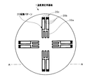
図1は温度測定用基板の平面図である。 FIG. 1 is a plan view of a temperature measurement substrate.
温度測定用基板1は基板10に配線パターン20が所望数だけ形成されてなる。配線パターン20は、ミアンダ状の配線からなる感熱部20aと、感熱部20aから引き出される4本のリード線20bと、リード線20bの端部に位置する端子20cと、からなる。端子20cは一対が電流端子とされ、一対が電圧端子とされる。端子20cは図示しない温度計測装置の端子に電気的に接続される。感熱部20aの配線には基板10の物理量すなわち温度やひずみ等に応じた電気信号が発生するが、その信号は温度計測装置で測定される。配線パターン20に設けられる配線を測温抵抗体として使用する場合には、温度計測装置は端子20cのうちの電流端子に通電し、感熱部20aにおける電圧降下を端子20cのうちの電圧端子で測定し、抵抗値を求めてその抵抗値に基づき温度を演算する。配線パターン20に設けられる配線を熱電対として使用する場合には、温度計測装置は端子20cのうちの電圧端子に生ずる熱起電力を測定し、温度を演算する。
The substrate for temperature measurement 1 is formed by forming a desired number of wiring patterns 20 on the substrate 10. The wiring pattern 20 includes a heat
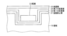
図2は第1の実施形態を示す図であって、図1のA−A断面のうち1本の配線パターン周辺の断面図に相当する。なお第1の実施形態において配線パターン20の断面構造はA−A断面に限らず図2のような構造である。 FIG. 2 is a diagram showing the first embodiment, and corresponds to a cross-sectional view around one wiring pattern in the AA cross section of FIG. 1. In the first embodiment, the cross-sectional structure of the wiring pattern 20 is not limited to the AA cross section, but is a structure as shown in FIG.
基板10の上面には配線パターン20に応じて溝11が形成される。そして溝11の内面及び基板10の上面に沿って薄膜状の拡散防止層21が積層される。この拡散防止層21の上面に沿って薄膜状の第1の密着層22が積層される。さらに溝11の内部では第1の密着層22の上面に沿って配線23が積層される。また配線23の上面に沿って薄膜状の第2の密着層24が積層される。そして第2の密着層24の上面には保護層25が積層される。このように基板10に形成された溝11には拡散防止層21、第1の密着層22、配線23、第2の密着層24、保護層25の順に埋設される。配線23は基板10に対して第1の密着層22で固定されており、接着剤や溶着剤は使用されていない。
A groove 11 is formed on the upper surface of the substrate 10 according to the wiring pattern 20. A thin-film
基板10は一般の半導体ウェーハと同じ材料で製造されており、例えばSiで形成される。ところで仮に基板10に配線23が直接接触すると、基板10の内部に配線23の成分が拡散する虞がある。そうした場合には基板10が変質して正確な温度を測定できなくなる。そこで第1の実施形態では基板10と配線23との間に拡散防止層21を介在させている。拡散防止層21は配線23の成分が基板10内に拡散することを防止する機能を有し、例えばSiO2、Cr2O3、Al2O3、AlN等の酸化膜や窒化膜で形成される。
The substrate 10 is made of the same material as a general semiconductor wafer, and is made of, for example, Si. However, if the
第1の実施形態では、基板10に配線23を固定するために、基板10と配線23との間に接着材や溶着剤の代わりに第1の密着層22を介在させており、また配線23に保護層25を固定するために、配線23と保護層25との間に第2の密着層24を介在させている。第1の密着層22は拡散防止層21を介して基板10に配線23を密着させる機能を有し、例えばTi、Cr、Al等の金属で形成される。第2の密着層24も第1の密着層22と同様に、例えばTi、Cr、Al等の金属で形成される。
In the first embodiment, in order to fix the
配線23は導電性を有する線材や箔材からなり、例えばCu、Pt、Au、Ag等の純金属や合金で形成される。配線23を測温抵抗体として使用する場合は、感熱部20aにおける長さを長くすることが望ましい。抵抗値が大きくなり測定しやすくなるためである。本実施形態ではその一例として感熱部20aの配線パターンをミアンダにしているが、他の形態、例えば円状にしてもよい。また配線23を熱電対として使用する場合は、異種金属を接合して配線23を形成する。この場合は感熱部20aに異種金属の接合点を配すればよく、測温抵抗体のように感熱部20aにおける長さを長くする必要はなく、配線パターンがミアンダである必要もない。
The
保護層25は配線23を覆うことによって、配線23の酸化や硫化を防止し、配線23を外部から絶縁し、配線23が外力を受けて損傷することを防止するものであり、また配線23を封止することによって配線23を基板20から剥離しにくくするものである。保護層25は、例えばエリンガムダイアグラムより選択したCr2O3、Al2O3、AlN等の酸化膜や窒化膜で形成される。
The
拡散防止層21、第1の密着層22、配線23、第2の密着層24、保護層25の材料の一例を示したが、各層の材料は他の層の材料に応じて最適なものを選択することが望ましい。同様に各層の厚さも最適な厚さを選択することが望ましい。各層間での材料の組み合わせには相性があり、その相性や層の厚み次第では各層の機能を高めることが可能であり、熱負荷時の反りを低減することが可能だからである。
Although an example of the material of the
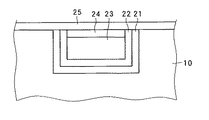
なお第1の実施形態では、少なくとも溝11の内部に拡散防止層21と第1の密着層22を介して配線23が埋設されていればよく、図3に示すように基板10の表面には必ずしも拡散防止層21や第1の密着層22や第2の密着層24や保護層25が積層されてなくてもよい。また保護層25が溝11に埋設されなくてもよい。つまり溝11の内部に拡散防止層21と第1の密着層22を介して配線23が埋設され、その配線23を第2の密着層24を介して保護層25が被覆しているのであれば、どのような形態であってもよい。
In the first embodiment, it is only necessary that the
第1の実施形態における温度測定用基板1は例えば次のようにして製造できる。先ず所望の配線パターン20に従って基板10の上面に溝11を形成し、形成した溝11及び基板10の上面に拡散防止層21と第1の密着層22と配線23と第2の密着層24を順に積層していき、化学機械研磨で余分な部分を研磨し、最後に被研磨面に保護層25を成膜することによって、溝11の内部に配線23を封止する。一例としては、デュアルダマシンプロセスのビアフィリングめっき技術を用いることができる。
The temperature measurement substrate 1 in the first embodiment can be manufactured, for example, as follows. First, the groove 11 is formed on the upper surface of the substrate 10 according to the desired wiring pattern 20, and the
第1の実施形態によれば、金属製の密着層で基板に配線を密着させ、また溝に配線を埋設しているため、接着剤や溶着剤を用いることなく基板に配線を固定することが可能になる。温度測定用基板には時間経過と共に形状や性質が変化する部材が用いられないため、部材の形状変化や性質変化に伴い温度測定値に誤差が生じることがなくなる。またそうした部材が用いられないため、基板から配線が剥離することもなくなる。 According to the first embodiment, since the wiring is in close contact with the substrate with the metal adhesion layer and the wiring is embedded in the groove, the wiring can be fixed to the substrate without using an adhesive or a welding agent. It becomes possible. Since a member whose shape and properties change with the passage of time is not used for the temperature measurement substrate, an error does not occur in the temperature measurement value due to the shape change or property change of the member. Further, since such a member is not used, the wiring does not peel off from the substrate.
また第1の実施形態によれば、接着剤が用いられないため接着層に起因する基板の反りが発生しなくなる。また各層の厚さ差を小さくすることができるため。したがって低反り測定用基板を実現できる。 Further, according to the first embodiment, since no adhesive is used, the warpage of the substrate due to the adhesive layer does not occur. Moreover, since the thickness difference of each layer can be made small. Therefore, a low warpage measurement substrate can be realized.
また接着剤を用いる場合は材料の厚さ制限があり、また成膜時の成膜速度をコントロールして低反り対応することができないが、第1の実施形態によれば、材料の厚さ制限がなく自由度が大きいため、成膜速度をコントロールして低反り対応することができる
第1の実施形態では基板10に形成された溝11に配線23等を埋設するようにしているが、溝11ではなく基板10の表面自体に配線23等を積層してもよい。そうした実施形態を第2の実施形態として説明する。
In addition, when an adhesive is used, there is a limitation on the thickness of the material, and it is impossible to cope with the low warp by controlling the deposition rate during deposition. However, according to the first embodiment, the thickness of the material is limited. In the first embodiment, the
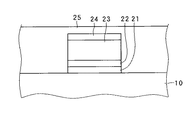
図4は第2の実施形態を示す図であって、図1のA−A断面のうち1本の配線パターン周辺の断面図に相当する。なお第2の実施形態において配線パターン20の断面構造はA−A断面に限らず図4のような構造である。 FIG. 4 is a diagram showing the second embodiment, and corresponds to a sectional view around one wiring pattern in the AA section of FIG. In the second embodiment, the cross-sectional structure of the wiring pattern 20 is not limited to the AA cross section, but is a structure as shown in FIG.
基板10にはその上面に沿って配線パターン20に応じた薄膜状の拡散防止層21が積層される。この拡散防止層21の上面に沿って薄膜状の第1の密着層22が積層される。さらに第1の密着層22の上面に沿って配線23が積層される。また配線23の上面に沿って薄膜状の第2の密着層24が積層される。そして配線23の上面及び基板10の上面には保護層25が積層される。このように基板10には拡散防止層21、第1の密着層22、配線23、第2の密着層24、保護層25が順に積層される。配線23は基板10に対して第1の密着層22で固定されており、接着剤や溶着剤は使用されていない。各層の機能及び材料は第1の実施形態と同じである。
A thin-film
第2の実施形態における温度測定用基板1は例えば次のようにして製造できる。先ず基板10の上面に拡散防止層21を成膜し、拡散防止層21の上面に第1の密着層22を成膜し、さらに第1の密着層22の上面に配線23を成膜し、またさらに配線23の上面に第2の密着層24を成膜し、エッチングやマイクロブラスト加工によって配線パターン20の分だけ各層を残し、最後に基板10の上面及び第2の密着層24の上面に保護層25を成膜して配線23を封止する。
The temperature measurement substrate 1 in the second embodiment can be manufactured as follows, for example. First, the
または、基板10にメタルマスクを施したうえで成膜や印刷によって配線パターン20に応じた拡散防止層21、第1の密着層22、配線23、第2の密着層24を積層し、基板10の上面及び第2の密着層24の上面に保護層25を成膜して配線23を封止するようにしてもよい。
Alternatively, after applying a metal mask to the substrate 10, the
第2の実施形態によれば、金属製の密着層で基板に配線を密着させているため、接着剤や溶着剤を用いることなく基板に配線を固定することが可能になる。温度測定用基板には時間経過と共に形状や性質が変化する部材が用いられないため、部材の形状変化や性質変化に伴い温度測定値に誤差が生じることがなくなる。またそうした部材が用いられないため、基板から配線が剥離することもなくなる。 According to the second embodiment, since the wiring is adhered to the substrate with the metal adhesion layer, the wiring can be fixed to the substrate without using an adhesive or a welding agent. Since a member whose shape and properties change with the passage of time is not used for the temperature measurement substrate, an error does not occur in the temperature measurement value due to the shape change or property change of the member. Further, since such a member is not used, the wiring does not peel off from the substrate.
また第2の実施形態によれば、接着剤が用いられないため接着層に起因する基板の反りが発生しなくなる。また各層の厚さ差を小さくすることができるため低反り測定用基板を実現できる。 Further, according to the second embodiment, since no adhesive is used, the warpage of the substrate due to the adhesive layer does not occur. In addition, since the thickness difference between the layers can be reduced, a low warpage measurement substrate can be realized.
また接着剤を用いる場合は材料の厚さ制限があり、また成膜時の成膜速度をコントロールして低反り対応することができないが、第2の実施形態によれば、材料の厚さ制限がなく自由度が大きいため、成膜速度をコントロールして低反り対応することができる
なお上記実施形態では本発明を温度測定用基板に適用した場合を説明したが、基板に設けた配線をひずみゲージとして使用する場合にも適用可能である。
In addition, when an adhesive is used, there is a limitation on the thickness of the material, and it is impossible to cope with the low warp by controlling the deposition rate during deposition. However, according to the second embodiment, the thickness of the material is limited. Since the degree of freedom is large and the degree of freedom can be controlled, it is possible to cope with low warpage by controlling the film formation rate. In the above embodiment, the case where the present invention is applied to a temperature measurement substrate has been described. It can also be applied when used as a gauge.
1…温度測定用基板、10…基板、11…溝、20…配線パターン、
21…拡散防止層、22…第1の密着層、23…配線、24…第2の密着層、
25…保護層
DESCRIPTION OF SYMBOLS 1 ... Temperature measurement board | substrate, 10 ... Board | substrate, 11 ... Groove, 20 ... Wiring pattern,
21 ... Diffusion prevention layer, 22 ... First adhesion layer, 23 ... Wiring, 24 ... Second adhesion layer,
25 ... Protective layer
Claims (6)
配線の成分が基板内に拡散することを防止する拡散防止層と、
配線の酸化及び硫化を防止する保護層と、
拡散防止層を介して基板に配線を密着させる金属製の第1の密着層と、
配線と保護層を密着させる金属製の第2の密着層と、
を備え、基板側から、拡散防止層、第1の密着層、配線、第2の密着層、保護層の順に積層したこと
を特徴とする測定用基板。 In a measurement substrate in which a physical quantity generated in a semiconductor substrate is measured through wiring provided on the substrate,
A diffusion preventing layer for preventing the wiring components from diffusing into the substrate;
A protective layer to prevent wiring oxidation and sulfuration;
A metal first adhesion layer that adheres the wiring to the substrate through the diffusion prevention layer;
A second adhesive layer made of metal that adheres the wiring and the protective layer;
A measurement substrate comprising a diffusion prevention layer, a first adhesion layer, a wiring, a second adhesion layer, and a protective layer laminated in this order from the substrate side.
を特徴とする請求項1記載の測定用基板。 The measurement substrate according to claim 1, wherein a groove is formed on the upper surface of the substrate, and a diffusion prevention layer, a first adhesion layer, a wiring, a second adhesion layer, and a protective layer are embedded in this groove in this order.
を特徴とする請求項1記載の測定用基板。 The diffusion prevention layer, the first adhesion layer, the wiring, and the second adhesion layer are laminated in this order on the upper surface of the substrate, and a protective layer is further laminated on the upper surface of the substrate and the upper surface of the second adhesion layer. Measurement board.
配線の成分が基板内に拡散することを防止する拡散防止層と、
配線の酸化及び硫化を防止する保護層と、
拡散防止層を介して基板に配線を密着させる金属製の第1の密着層と、
配線と保護層を密着させる金属製の第2の密着層と、
を備え、基板側から、拡散防止層、第1の密着層、配線、第2の密着層、保護層の順に積層したこと
を特徴とする温度測定用基板。 In a temperature measurement substrate provided with a wiring having a heat sensitive part on a semiconductor substrate,
A diffusion preventing layer for preventing the wiring components from diffusing into the substrate;
A protective layer to prevent wiring oxidation and sulfuration;
A metal first adhesion layer that adheres the wiring to the substrate through the diffusion prevention layer;
A second adhesive layer made of metal that adheres the wiring and the protective layer;
A temperature measurement substrate comprising: a diffusion preventing layer, a first adhesion layer, a wiring, a second adhesion layer, and a protective layer, which are laminated in this order from the substrate side.
を特徴とする請求項4記載の温度測定用基板。 The substrate for temperature measurement according to claim 4, wherein a groove is formed on the upper surface of the substrate, and a diffusion preventing layer, a first adhesion layer, a wiring, a second adhesion layer, and a protective layer are embedded in this groove in this order.
を特徴とする請求項4記載の温度測定用基板。 5. The diffusion prevention layer, the first adhesion layer, the wiring, and the second adhesion layer are sequentially laminated on the upper surface of the substrate, and a protective layer is further laminated on the upper surface of the substrate and the upper surface of the second adhesion layer. Temperature measurement board.
Priority Applications (1)
| Application Number | Priority Date | Filing Date | Title |
|---|---|---|---|
| JP2007293147A JP5135630B2 (en) | 2007-11-12 | 2007-11-12 | Measurement board and temperature measurement board |
Applications Claiming Priority (1)
| Application Number | Priority Date | Filing Date | Title |
|---|---|---|---|
| JP2007293147A JP5135630B2 (en) | 2007-11-12 | 2007-11-12 | Measurement board and temperature measurement board |
Publications (2)
| Publication Number | Publication Date |
|---|---|
| JP2009123744A true JP2009123744A (en) | 2009-06-04 |
| JP5135630B2 JP5135630B2 (en) | 2013-02-06 |
Family
ID=40815620
Family Applications (1)
| Application Number | Title | Priority Date | Filing Date |
|---|---|---|---|
| JP2007293147A Expired - Fee Related JP5135630B2 (en) | 2007-11-12 | 2007-11-12 | Measurement board and temperature measurement board |
Country Status (1)
| Country | Link |
|---|---|
| JP (1) | JP5135630B2 (en) |
Cited By (2)
| Publication number | Priority date | Publication date | Assignee | Title |
|---|---|---|---|---|
| WO2017200267A1 (en) * | 2016-05-16 | 2017-11-23 | 한국표준과학연구원 | Temperature measurement wafer sensor and method for manufacturing same |
| CN120538689A (en) * | 2025-05-23 | 2025-08-26 | 云浮荣发科技有限公司 | A thin film platinum resistance sensor and its preparation method and application |
Citations (7)
| Publication number | Priority date | Publication date | Assignee | Title |
|---|---|---|---|---|
| JPS62165336A (en) * | 1986-01-14 | 1987-07-21 | Nec Corp | Temperature-measuring wafer |
| JPH06310580A (en) * | 1993-04-20 | 1994-11-04 | Nippon Steel Corp | Semiconductor wafer having temperature measuring method and temperature measuring means |
| JPH06331454A (en) * | 1993-05-25 | 1994-12-02 | Hitachi Ltd | Temperature measuring device |
| JPH07311095A (en) * | 1994-01-12 | 1995-11-28 | Texas Instr Inc <Ti> | Structure of wafer for calibrating temperature sensor and manufacture thereof |
| JPH11297699A (en) * | 1998-04-14 | 1999-10-29 | Sony Corp | Diffusion barrier layer and method of manufacturing the same |
| JPH11340233A (en) * | 1998-05-29 | 1999-12-10 | Nec Corp | Formation of copper wiring |
| WO2007006640A1 (en) * | 2005-07-12 | 2007-01-18 | Max Bögl Bauunternehmung GmbH & Co. KG | Fixed running track on a bridge structure |
-
2007
- 2007-11-12 JP JP2007293147A patent/JP5135630B2/en not_active Expired - Fee Related
Patent Citations (7)
| Publication number | Priority date | Publication date | Assignee | Title |
|---|---|---|---|---|
| JPS62165336A (en) * | 1986-01-14 | 1987-07-21 | Nec Corp | Temperature-measuring wafer |
| JPH06310580A (en) * | 1993-04-20 | 1994-11-04 | Nippon Steel Corp | Semiconductor wafer having temperature measuring method and temperature measuring means |
| JPH06331454A (en) * | 1993-05-25 | 1994-12-02 | Hitachi Ltd | Temperature measuring device |
| JPH07311095A (en) * | 1994-01-12 | 1995-11-28 | Texas Instr Inc <Ti> | Structure of wafer for calibrating temperature sensor and manufacture thereof |
| JPH11297699A (en) * | 1998-04-14 | 1999-10-29 | Sony Corp | Diffusion barrier layer and method of manufacturing the same |
| JPH11340233A (en) * | 1998-05-29 | 1999-12-10 | Nec Corp | Formation of copper wiring |
| WO2007006640A1 (en) * | 2005-07-12 | 2007-01-18 | Max Bögl Bauunternehmung GmbH & Co. KG | Fixed running track on a bridge structure |
Cited By (2)
| Publication number | Priority date | Publication date | Assignee | Title |
|---|---|---|---|---|
| WO2017200267A1 (en) * | 2016-05-16 | 2017-11-23 | 한국표준과학연구원 | Temperature measurement wafer sensor and method for manufacturing same |
| CN120538689A (en) * | 2025-05-23 | 2025-08-26 | 云浮荣发科技有限公司 | A thin film platinum resistance sensor and its preparation method and application |
Also Published As
| Publication number | Publication date |
|---|---|
| JP5135630B2 (en) | 2013-02-06 |
Similar Documents
| Publication | Publication Date | Title |
|---|---|---|
| JP4952428B2 (en) | Sensor device | |
| KR101412951B1 (en) | Resistor and method for manufacturing the same | |
| KR20170101794A (en) | Semiconductor pressure sensor for harsh media application | |
| TW201248769A (en) | Methods and apparatus for a multi-zone pedestal heater | |
| JP6804646B2 (en) | Semiconductor module | |
| US12504335B2 (en) | Sensor element and method for manufacturing a sensor element | |
| JP5125978B2 (en) | Sensor device | |
| JPWO2020032021A1 (en) | Temperature sensor and device equipped with temperature sensor | |
| EP0460785B1 (en) | Semiconductor device having a heat sink | |
| JP5135630B2 (en) | Measurement board and temperature measurement board | |
| US7893345B2 (en) | Thermoelectric module device | |
| WO2014002737A1 (en) | Thermal airflow sensor | |
| JP2013164332A (en) | Pressure sensor module | |
| JP4547475B2 (en) | Flat plate temperature sensor | |
| WO2014156273A1 (en) | Dynamic-quantity measurement device and manufacturing method therefor | |
| JP6129980B2 (en) | Mechanical quantity measuring apparatus and manufacturing method thereof | |
| JPH10185725A (en) | Electrode structure of semiconductor device and method of manufacturing the same | |
| JP2013052449A (en) | Mems sensor | |
| CN116190324A (en) | Stress-relief layers based on coating technology | |
| JP2008270599A (en) | Metal plate resistor | |
| JP5779487B2 (en) | Pressure sensor module | |
| JP4978294B2 (en) | Semiconductor device and manufacturing method thereof | |
| JP6208098B2 (en) | Semiconductor element connection unit and mechanical quantity measuring apparatus having the same | |
| JP2010008225A (en) | Thermal flow sensor and manufacturing method thereof | |
| JP3510803B2 (en) | Flow rate detecting device and manufacturing method thereof |
Legal Events
| Date | Code | Title | Description |
|---|---|---|---|
| A625 | Written request for application examination (by other person) |
Free format text: JAPANESE INTERMEDIATE CODE: A625 Effective date: 20101019 |
|
| A977 | Report on retrieval |
Free format text: JAPANESE INTERMEDIATE CODE: A971007 Effective date: 20120222 |
|
| A131 | Notification of reasons for refusal |
Free format text: JAPANESE INTERMEDIATE CODE: A131 Effective date: 20120515 |
|
| A521 | Request for written amendment filed |
Free format text: JAPANESE INTERMEDIATE CODE: A523 Effective date: 20120628 |
|
| TRDD | Decision of grant or rejection written | ||
| A01 | Written decision to grant a patent or to grant a registration (utility model) |
Free format text: JAPANESE INTERMEDIATE CODE: A01 Effective date: 20120731 |
|
| A61 | First payment of annual fees (during grant procedure) |
Free format text: JAPANESE INTERMEDIATE CODE: A61 Effective date: 20120824 |
|
| A61 | First payment of annual fees (during grant procedure) |
Free format text: JAPANESE INTERMEDIATE CODE: A61 Effective date: 20121025 |
|
| R150 | Certificate of patent or registration of utility model |
Free format text: JAPANESE INTERMEDIATE CODE: R150 Ref document number: 5135630 Country of ref document: JP Free format text: JAPANESE INTERMEDIATE CODE: R150 |
|
| FPAY | Renewal fee payment (event date is renewal date of database) |
Free format text: PAYMENT UNTIL: 20151122 Year of fee payment: 3 |
|
| FPAY | Renewal fee payment (event date is renewal date of database) |
Free format text: PAYMENT UNTIL: 20151122 Year of fee payment: 3 |
|
| R250 | Receipt of annual fees |
Free format text: JAPANESE INTERMEDIATE CODE: R250 |
|
| R250 | Receipt of annual fees |
Free format text: JAPANESE INTERMEDIATE CODE: R250 |
|
| R250 | Receipt of annual fees |
Free format text: JAPANESE INTERMEDIATE CODE: R250 |
|
| R250 | Receipt of annual fees |
Free format text: JAPANESE INTERMEDIATE CODE: R250 |
|
| R250 | Receipt of annual fees |
Free format text: JAPANESE INTERMEDIATE CODE: R250 |
|
| R250 | Receipt of annual fees |
Free format text: JAPANESE INTERMEDIATE CODE: R250 |
|
| R250 | Receipt of annual fees |
Free format text: JAPANESE INTERMEDIATE CODE: R250 |
|
| R250 | Receipt of annual fees |
Free format text: JAPANESE INTERMEDIATE CODE: R250 |
|
| R250 | Receipt of annual fees |
Free format text: JAPANESE INTERMEDIATE CODE: R250 |
|
| LAPS | Cancellation because of no payment of annual fees |